EP1223676A2 - Automatic bias adjustment circuit for use in PLL circuit - Google Patents
Automatic bias adjustment circuit for use in PLL circuit Download PDFInfo
- Publication number
- EP1223676A2 EP1223676A2 EP01309826A EP01309826A EP1223676A2 EP 1223676 A2 EP1223676 A2 EP 1223676A2 EP 01309826 A EP01309826 A EP 01309826A EP 01309826 A EP01309826 A EP 01309826A EP 1223676 A2 EP1223676 A2 EP 1223676A2
- Authority
- EP
- European Patent Office
- Prior art keywords
- bias
- current
- circuit
- voltage
- adjustment
- Prior art date
- Legal status (The legal status is an assumption and is not a legal conclusion. Google has not performed a legal analysis and makes no representation as to the accuracy of the status listed.)
- Granted
Links
Images






Classifications
-
- H—ELECTRICITY
- H03—ELECTRONIC CIRCUITRY
- H03L—AUTOMATIC CONTROL, STARTING, SYNCHRONISATION OR STABILISATION OF GENERATORS OF ELECTRONIC OSCILLATIONS OR PULSES
- H03L7/00—Automatic control of frequency or phase; Synchronisation
- H03L7/06—Automatic control of frequency or phase; Synchronisation using a reference signal applied to a frequency- or phase-locked loop
- H03L7/08—Details of the phase-locked loop
- H03L7/0805—Details of the phase-locked loop the loop being adapted to provide an additional control signal for use outside the loop
-
- H—ELECTRICITY
- H03—ELECTRONIC CIRCUITRY
- H03L—AUTOMATIC CONTROL, STARTING, SYNCHRONISATION OR STABILISATION OF GENERATORS OF ELECTRONIC OSCILLATIONS OR PULSES
- H03L1/00—Stabilisation of generator output against variations of physical values, e.g. power supply
- H03L1/02—Stabilisation of generator output against variations of physical values, e.g. power supply against variations of temperature only
- H03L1/022—Stabilisation of generator output against variations of physical values, e.g. power supply against variations of temperature only by indirect stabilisation, i.e. by generating an electrical correction signal which is a function of the temperature
-
- H—ELECTRICITY
- H03—ELECTRONIC CIRCUITRY
- H03L—AUTOMATIC CONTROL, STARTING, SYNCHRONISATION OR STABILISATION OF GENERATORS OF ELECTRONIC OSCILLATIONS OR PULSES
- H03L7/00—Automatic control of frequency or phase; Synchronisation
- H03L7/06—Automatic control of frequency or phase; Synchronisation using a reference signal applied to a frequency- or phase-locked loop
- H03L7/08—Details of the phase-locked loop
- H03L7/10—Details of the phase-locked loop for assuring initial synchronisation or for broadening the capture range
- H03L7/101—Details of the phase-locked loop for assuring initial synchronisation or for broadening the capture range using an additional control signal to the controlled loop oscillator derived from a signal generated in the loop
-
- H—ELECTRICITY
- H03—ELECTRONIC CIRCUITRY
- H03L—AUTOMATIC CONTROL, STARTING, SYNCHRONISATION OR STABILISATION OF GENERATORS OF ELECTRONIC OSCILLATIONS OR PULSES
- H03L7/00—Automatic control of frequency or phase; Synchronisation
- H03L7/06—Automatic control of frequency or phase; Synchronisation using a reference signal applied to a frequency- or phase-locked loop
- H03L7/16—Indirect frequency synthesis, i.e. generating a desired one of a number of predetermined frequencies using a frequency- or phase-locked loop
- H03L7/18—Indirect frequency synthesis, i.e. generating a desired one of a number of predetermined frequencies using a frequency- or phase-locked loop using a frequency divider or counter in the loop
- H03L7/183—Indirect frequency synthesis, i.e. generating a desired one of a number of predetermined frequencies using a frequency- or phase-locked loop using a frequency divider or counter in the loop a time difference being used for locking the loop, the counter counting between fixed numbers or the frequency divider dividing by a fixed number
- H03L7/187—Indirect frequency synthesis, i.e. generating a desired one of a number of predetermined frequencies using a frequency- or phase-locked loop using a frequency divider or counter in the loop a time difference being used for locking the loop, the counter counting between fixed numbers or the frequency divider dividing by a fixed number using means for coarse tuning the voltage controlled oscillator of the loop
- H03L7/189—Indirect frequency synthesis, i.e. generating a desired one of a number of predetermined frequencies using a frequency- or phase-locked loop using a frequency divider or counter in the loop a time difference being used for locking the loop, the counter counting between fixed numbers or the frequency divider dividing by a fixed number using means for coarse tuning the voltage controlled oscillator of the loop comprising a D/A converter for generating a coarse tuning voltage
-
- H—ELECTRICITY
- H03—ELECTRONIC CIRCUITRY
- H03L—AUTOMATIC CONTROL, STARTING, SYNCHRONISATION OR STABILISATION OF GENERATORS OF ELECTRONIC OSCILLATIONS OR PULSES
- H03L7/00—Automatic control of frequency or phase; Synchronisation
- H03L7/06—Automatic control of frequency or phase; Synchronisation using a reference signal applied to a frequency- or phase-locked loop
- H03L7/08—Details of the phase-locked loop
- H03L7/085—Details of the phase-locked loop concerning mainly the frequency- or phase-detection arrangement including the filtering or amplification of its output signal
- H03L7/089—Details of the phase-locked loop concerning mainly the frequency- or phase-detection arrangement including the filtering or amplification of its output signal the phase or frequency detector generating up-down pulses
- H03L7/0891—Details of the phase-locked loop concerning mainly the frequency- or phase-detection arrangement including the filtering or amplification of its output signal the phase or frequency detector generating up-down pulses the up-down pulses controlling source and sink current generators, e.g. a charge pump
- H03L7/0893—Details of the phase-locked loop concerning mainly the frequency- or phase-detection arrangement including the filtering or amplification of its output signal the phase or frequency detector generating up-down pulses the up-down pulses controlling source and sink current generators, e.g. a charge pump the up-down pulses controlling at least two source current generators or at least two sink current generators connected to different points in the loop
Definitions
- the present invention relates generally to a PLL (Phase-Locked Loop) circuit, more particularly, to an automatic bias adjustment circuit adjusting a bias current provided to a CCO (Current Controlled Oscillator).
- PLL Phase-Locked Loop
- CCO Current Controlled Oscillator
- FIG. 8 shows a schematic configuration of a prior art voltage controlled oscillator (VCO) 10 for use in a PLL circuit.
- VCO voltage controlled oscillator
- a control voltage VC is converted into a current IE by a V/I converter circuit 11, and the current IE is added to a bias current IB by an adder 12 to make a control current IC, which is provided to a current-controlled oscillator (CCO) 13.
- the CCO 13 outputs an oscillation clock OCLK with a frequency FO according to the value of the control current IC.
- the characteristics vary greatly with variations in fabrication process conditions, that is, variations in threshold voltage, gate length and gate insulating film thickness of FETs which are constituents of the VCO 10.
- a characteristic curve TYP in the figure is of a typical case, while other characteristic curves POW and SPW are of cases where the oscillation frequency FO are equal to the maximum and the minimum, respectively, for each control voltage VC because of variations in the fabrication process conditions.
- the control voltage VC is an output of a loop filter.
- the range of variable frequencies VL to VH of the output is usually determined by a power supply voltage and the threshold of FETs.
- a frequency Fm is equal to a reference clock frequency when the control voltage VC is equal to the middle value Vm between VL and VH
- the range of a frequency of the VCO 10 in which the frequency can vary in the PLL circuit is maximized.
- the VCO 10 is designed in this way, the VCO 10 is apt to become out of lock due to noise or a variation in clock frequency since the range of the frequency in which it can vary is narrow in a case where the frequency characteristic thereof is of POW according to variations in the fabrication process conditions. Meanwhile, where the frequency characteristic thereof is of SPW, the VCO 10 cannot achieve the in lock condition.
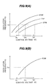
- the characteristics of the VCO 10 are also dependent on temperature as shown in FIG. 10(A). Characteristic curves in the figure show ones in cases where temperatures are T1, T2 and T3 wherein a relation T1 ⁇ T2 ⁇ T3 is satisfied.
- FIG. 10(B) shows a relationship between temperature T and the oscillation frequency FO under the condition that the control voltage VC is at a constant value.
- the VCO gain is small as shown in FIG. 10(A), the range of variable frequencies and a margin in the PLL circuit are narrow; therefore, a more exact adjustment of the bias current IB is required to avoid the VCO becoming out of lock due to variations in temperature and noise.
- JP 10-84278 A a PLL circuit employing a replica of a CCO is used as an automatic bias adjustment circuit, and the output of a V/I converter circuit in a VCO is used as a bias current IB to the PLL circuit, which is an adjustment object, to deal with variations in process conditions and temperature.
- the VCO gain of the PLL circuit to be adjusted is reduced to restrict jitter to a low value
- the VCO gain of the bias adjustment circuit is also reduced; therefore, the out of lock condition can arise in the bias adjustment circuit, thereby preventing a proper bias current IB from being generated.
- JP 11-177416 A in order to cope with variations in process conditions and temperature, the output of a loop filter is converted into a current by a D/A converter circuit to use the current as a bias current IB.
- the bias current IB is proportional to the control voltage VC in this case, the control current of the CCO is also proportional to the control voltage VC; therefore the control current IC cannot be set to a value at the middle point of its range against variations in process conditions and temperature.
- JP 10-70458 A in order to cope with variations in process conditions and temperature, the output voltage of a loop filter is compared with a reference voltage having a temperature coefficient of almost zero, the count value of a counter is changed in accordance with the result of the comparison, and a bias switch is controlled by the count value to determine the state of a bias generator.
- an automatic bias adjustment circuit capable of giving a more proper bias current to a PLL circuit against variations in process conditions and temperature.
- An automatic bias adjustment circuit is for use in a PLL circuit.
- the PLL circuit is provided with voltage-controlled oscillator comprising: a voltage to current converter circuit converting a control voltage VC to a current IE; and a current-controlled oscillator receiving a control current IC which is obtained by adding a bias current IB to the converted current IE.
- the bias current IB is the sum of a first bias current adjusted for dealing with process variations and a second bias current for dealing with temperature variation. These first and second bias currents are generated by a bias adjustment circuit and a bias current generating circuit, respectively.
- the bias adjustment circuit adjusts the first bias current in response to an adjustment start signal such that the control voltage converges to a reference voltage, and ceases the adjustment when the convergence has been achieved.
- the reference voltage is determined to be an almost middle point in the range of the variable control voltage.
- the bias current generating circuit provides the second bias current having such a temperature characteristic that the control voltage is prevented from shifting from the reference voltage due to temperature variation.
- the adjustment by the bias adjustment circuit is not performed after the first bias current has been adjusted such that the control voltage converges to the reference voltage, even if the characteristics of the voltage-controlled oscillator change due to variation in temperature, the value of the first bias current does not rapidly change, thereby ensuring a stable operation of the PLL circuit.
- the control voltage is maintained at an almost middle point in the range of the variable control voltage.
- the frequency range within which the VCO remains in lock becomes almost the maximum independently of variation in temperature, and therefore even if the VCO gain is reduced in design in order to minimize jitter due to noise, the out of lock condition can be prevented.
- the bias current generating circuit is constituted of a bias voltage generating circuit and a voltage to current converter circuit converting a generated bias voltage to a current which is the second bias current
- the bias voltage generating circuit generates a bias voltage having a temperature characteristic opposite to that of the control voltage under the condition that the frequency of the oscillation signal is fixed.
- Another aspect of the invention provides a bias adjustment method for adjusting a bias current for a PLL circuit.
- FIG. 1 shows a PLL circuit of a first embodiment according to the present invention.
- a VCO 10 has the same configuration as the VCO 10 of FIG. 8 and an oscillation clock OCLK with a frequency FO of the VCO 10 is provided to a divider by N, 14, to generate a feedback clock FCLK with a frequency FO/N.
- a phase comparator 15 detects lag or lead of the feedback clock FCLK with respect to a reference clock RCLK to generate a pulse of an up signal UP or a down signal DWN at each time of the lag or lead detection.
- a charge pump circuit 16 charges or discharges a filter capacitor in a loop filter 17 in response to a pulse of the up signal UP or the down signal DWN, respectively.
- the output of the loop filter 17 is given as a control voltage VC to a V/I converter circuit 11 of the VCO 10.
- the frequency of the reference clock RCLK is usually shifted from a nominal frequency by variations in process conditions for its generating circuit and variation in temperature.
- An automatic bias adjustment circuit giving a bias current IB to an adder 12 is added to the PLL circuit constituted of the VCO 10, the divider by N, 14, the phase comparator 15, the charge pump circuit 16, and the loop filter 17. Next, description will be given of this adjustment circuit.
- the bias current IB is the sum of a bias current IB1 adjusted for coping with variations in process conditions and a bias current IB2 for coping with variation in temperature.
- bias adjustment circuit (18, 19, 20, 21 and 22) generating a bias current IB1.
- the control voltage VC is compared with a reference voltage VREF generated at a reference voltage generating circuit 18 by a comparator 19.
- the reference voltage generating circuit 18 is designed such that the output VREF thereof is equal to a value at the middle point in the range of the variable output voltage of the loop filter 17, that is, Vm of FIG. 10(A).
- this range of variable output voltage extends from Vth to (VDD - Vth), for example, from 0.2 to 1.6 V, where VDD is a power supply voltage and Vth is a threshold voltage of a FET.
- VREF VDD/2, which can be generated by a well-known voltage divider.
- the comparison result CR of the comparator 19 is high when VC > VREF, while being low when VC ⁇ VREF.
- the comparison result CR is provided to a register setting circuit 20 together with the reference clock RCLK and an adjustment start signal ADJ.
- the operation of the register setting circuit 20 is started by a pulse of the adjustment start signal ADJ given thereto and operates in synchronism with a clock obtained by dividing the reference clock RCLK.
- the register setting circuit 20 sets values SV to a register 21 so that a series of comparison results CR shows convergence of VC to VREF, and after the convergence, fixes the set value SV.
- the register setting circuit 20 sets '1' to a selected bit as a test bit in the register 21 sequentially from the most significant bit to the least significant bit at predetermined cycles, and after setting or resetting the least significant bit, fixes the contents of the register 21.
- An output value SV1 of the register 21 is converted into the bias current IB1 by a D/A converter circuit 22.
- the D/A converter circuit 22 can be constructed by connecting a plurality of circuits, each having a serial connection of a constant current source and a switching transistor, in parallel to each other. On and off of each switching transistor is determined by the set value SV1.
- a bias voltage VT generated at a bias voltage generating circuit 23 is converted into the bias current IB2 by a V/I converter circuit 24.
- the bias voltage generating circuit 23 is designed such that the bias voltage VT shows a temperature characteristic as described later.
- each of the adders 25 and 12 can be constructed of a simple wire connection.
- the circuit of FIG. 1 is formed in a semiconductor integrated circuit device, wherein the loop filter 17 may be externally provided for reduction in chip area.
- FIG. 2 shows an embodiment of the register setting circuit 20 of FIG. 1 together with the register 21.
- An RS flip-flop 30 is set by a pulse of the adjustment start signal ADJ and the non-inverting output thereof is provided to one input of an AND gate 31.
- a pulse of the adjustment start signal ADJ is generated by a circuit(not shown)when power is turned on.
- the reference clock RCLK is provided to the other input of the AND gate 31.
- the reference clock RCLK passes through the AND gate 31 when the RS flip-flop 30 is in a set state and the passed clock RCLK is provided to a divider by M, 32, to generate an operating clock CKL1 in order to place the circuits 20 and 21 into an operating state, wherein M is determined such that a half cycle of the clock CLK1 is longer than a time from the reference clock RCLK being provided to the PLL circuit of FIG. 1 till the PLL circuit becoming in lock.
- the clock CLK1 is provided to one input of an AND gate 33 and the comparison result CR is provided to the other input thereof.
- the output of the AND gate 33 is provided to one input of each of AND gates 40 to 43.
- the clock CLK1 is also provided to the clock input CK of a counter 44 and a three bit count CV thereof is provided to a decoder 45 to be decoded.
- the decoder 45 has 5 outputs each going '1' when the count CV has a corresponding one of values 0 to 4.
- the clock CLK1 is further provided through a delay circuit 46 to one input of each of AND gates 50 to 53 as a clock CLK2.
- the outputs of the AND gates 40 to 43 are provided to first inputs of respective OR gates 60 to 63, and to the other inputs of the respective OR gates 60 to 63, there are provided respective bits of a 4 bit shift register 64, for outputting a test bit, in the order from the least to most significant bits.
- the shift register 64 is set to '1000' in response to a pulse of the adjustment start signal ADJ.
- the clock CLK1 is provided to the clock input CK of the shift register 64, and the '1' (test bit) thereof is shifted to the right and '0' is loaded at the least significant bit thereof every rise of the clock CLK1.
- the outputs of the OR gates 60 to 63 are provided to data inputs of respective D flip-flops 70 to 73 of the register 21, and the outputs of OR gates 80 to 83 are provided to the clock inputs of the D flip-flops 70 to 73.
- To the OR gate 80 there are provided a signal obtained by passing the adjustment start signal ADJ through a delay circuit 84 and the output of the AND gate 50.
- To the OR gate 81 there are provided the outputs of the AND gates 50 and 51.
- To the OR gate 82 there are provided the outputs of the AND gates 51 and 52.
- To the OR gate 83 there are provided the outputs of the AND gates 52 and 53.
- FIG. 3 is a time chart showing operation of the circuit of FIG. 2.
- each of the five outputs of the decoder 45 is '0.'
- a value of the register 21 is set by the register setting circuit 20 such that the control voltage VC converges to the reference voltage VREF, and the actual use of the PLL circuit is started.
- the set value SV1 is not changed even if characteristics of the CCO 13 change due to a variation in temperature after the setting, the value of the bias current IB does not rapidly change during the use of the PLL circuit, thereby ensuring a stable operation of the PLL circuit.
- characteristics of an analog circuit have temperature dependency.
- characteristics of the CCO 13 have a large influence of temperature in comparison with those of the V/I converter circuit 11 and the loop filter 17 which are analog circuits. Therefore, with change in temperature, the PLL circuit operates so as to stay in lock, and as a result the control voltage VC shifts from the value at the middle point of a range of the variable control voltage VC.
- the VCO 10 reduces the oscillation frequency FO as shown in FIG. 10(B).
- a current IC increases by ⁇ IC, that is, the control voltage VC increases to operate such that the frequency of the feedback clock FCLK coincides with that of the reference clock RCLK. Therefore, the temperature characteristic of the bias voltage generating circuit 23 is determined by design such that the bias current IB2 increases by ⁇ IC with increase in temperature by ⁇ T.
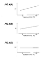
- the output voltage VT of the bias voltage generating circuit 23 has a temperature characteristic opposite to that of the control voltage VC under the condition that the frequency FO of the oscillation clock OCLK is fixed in regard to the VCO 10.
- FIG. 4(A) shows changes in bias voltage VT versus temperature.
- the control voltage VC is maintained at a value of an almost middle point in the range of the variable control voltage VC, and thereby the range of the variable oscillation frequency FO becomes almost the maximum in spite of change in temperature, thereby preventing out of lock from occurring even with a small VCO gain designed for reducing jitter due to noise.
- a digital automatic bias adjustment circuit was operated at all times in order to deal with variation in temperature.
- the digital bias adjustment circuit ceases its operation after the initial adjustment, power consumption can be reduced and the lifetime of a battery can be extended when the PLL circuit is employed especially in mobile electronic equipment such as a portable telephone.
- the CCO 13 may have a temperature characteristic which is the reverse of (opposite to) FIG. 10(B), whereby it is only required that the temperature characteristic of the bias voltage generating circuit 23 is reversed according to such circumstances.
- the slope of temperature characteristic of the bias voltage generating circuit 23 can be properly set to a positive coefficient or a negative coefficient.
- a resistor and a constant current source are connected in series between a power supply line and ground, a voltage at a connection node between the resistor and the constant current source can be taken out as the bias voltage VT, then the bias voltage VT has a temperature characteristic of the resistor.
- the temperature characteristic of the bias voltage VT is reversed.
- a voltage across a diode through which a forward current flows is employed instead of the resistor, the same effect can be exerted.
- the temperature characteristic of the bias voltage VT can be close to a more preferable one.
- FIG. 5 shows a PLL circuit of a second embodiment according to the present invention.
- the bias voltage generating circuit 23 of FIG. 1 is omitted and the output of a reference voltage generating circuit 18A is provided to a V/I converter circuit 24A.
- the reference voltage generating circuit 18A has such a temperature characteristic that the above-described temperature compensation is performed for the control voltage VC.
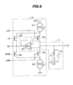
- FIG. 6 shows an embodiment of a charge pump circuit 16 and a loop filter 17 employed in a PLL circuit, of a third embodiment according to the present invention.
- a constant current source 161, a PMOS transistor 162, an NMOS transistor 163 and a constant current source 164 are connected in series between VDD and ground.
- a PMOS transistor 165 and an NMOS transistor 166 are connected in series between the sources of the PMOS transistor 162 and the MOS transistor 163.
- the charge pump circuit 16 has a characteristic in that the input of a voltage follower circuit 167 is connected to the drain (a voltage VC) of the PMOS transistor 162, the output of the voltage follower circuit 167 is connected to the drain of the PMOS transistor 165, and the output voltage VD thereof is provided to the non-inverting input of the comparator 19 of FIG. 1 or 5.
- the up signal UP and the down signal DWN are provided to the gates of the PMOS transistor 165 and the NMOS transistor 163, respectively, and the inverted signals *UP and *DWN of the signals UP and DWN are provided to the gates of the PMOS transistor 162 and the NMOS transistor 166.
- the loop filter 17 has a well-known configuration in which a resistor 171 and a filter capacitor 172 are connected in series between the output of the charge pump circuit 16 and ground and a phase compensation filter capacitor 173 is connected in parallel thereto.
- the voltage follower circuit 167 is not only a constituent of the charge pump circuit 16, but also a constituent of the loop filter 17. That is, the voltage follower circuit 167 also serves as a voltage output buffer circuit in the loop filter 17.
- the PMOS transistor 162 By a positive pulse of the up signal UP, the PMOS transistor 162 is turned on while the PMOS transistor 165 is turned off to output the current I through the PMOS transistor 162 and charge the filter capacitors 172 and 173. Since, at this time, the NMOS transistor 163 is off but the NMOS transistor 166 is on, the current I can be taken out from the output of the voltage follower circuit 167 by the constant current source 164.
- FIG. 7 shows voltage waveforms of signals VD and VC in relation to a pulse of the up signal UP.
- the NMOS transistor 163 is turned on, while the NMOS transistor 166 is turned off to discharge part of the electric charge on the filter capacitors 172 and 173 through the NMOS transistor 163 and the constant current source 164.
- the PMOS transistor 162 is off, since the PMOS transistor 165 is on, the current I flowing through the constant current source 161 flows into the input of the voltage follower circuit 167.
- a configuration may be adopted in which the output VD of the voltage follower 167 of FIG. 6 is provided to the VCO 10 as the control voltage.
- phase comparator 15 outputs an analog error signal
- charge pump circuit 16 a combination of the digital phase comparator 15 and the charge pump circuit 16 can be regarded as an analog phase comparator
- the automatic bias adjustment circuit of the present invention can be applied to a PLL circuit with no divider by N, 14.
- the register setting circuit 20 may be of a configuration in which the set value SV is sequentially incremented or decremented.
- the addition of the first bias and the second bias may be performed on a signal line between the loop filter 17 and the CCO 13. That is, the addition may be performed on the input side of the V/I converter 11 instead of the output side thereof. In this case, since the operation is addition of voltages, the V/I converter circuit 24 is omitted and the D/A converter has a voltage output. Further, addition of one of the first bias and the second bias to the signal line between the circuits 17 and 13 may be performed on the input side of the V/I converter circuit 11 and addition of the other thereof may be performed on the output side of the V/I converter circuit 11.
- the reference signal is not required to be a clock signal, but may be a data signal generated in synchronism with a clock signal.
Landscapes
- Stabilization Of Oscillater, Synchronisation, Frequency Synthesizers (AREA)
Abstract
Description
Claims (19)
- An automatic bias adjustment circuit adjusting a bias current for a PLL circuit which includes: a loop filter; a voltage to current converter circuit converting an output voltage of said loop filter as a control voltage to a current; and a current-controlled oscillator, receiving a control current which is obtained by adding said bias current to said converted current, said bias current being a sum of first and second bias currents, generating an oscillation signal responsive to said control current;
wherein said PLL circuit operates so that said oscillation signal or a signal obtained by dividing said oscillation signal is locked on a reference signal received, said automatic bias adjustment circuit comprising:a bias adjustment circuit, providing said first bias current, adjusting said first bias current in response to an adjustment start signal such that said control voltage converges to a reference voltage; anda bias current generating circuit, providing said second bias current which changes with temperature such that said control voltage is prevented from shifting from said reference voltage due to temperature variation. - The automatic bias adjustment circuit of claim 1,
wherein said bias adjustment circuit ceases the adjustment when the convergence has been achieved. - The automatic bias adjustment circuit of claim 2,
wherein said bias current generating circuit comprises:a bias voltage generating circuit generating a bias voltage which has a temperature characteristic opposite to that of said control voltage; anda voltage to current converter circuit converting said bias voltage to a current which is said second bias current. - The automatic bias adjustment circuit of claim 2, further comprising: a reference voltage generating circuit generating said reference voltage which has a temperature characteristic opposite to that of said control voltage under a condition that a frequency of said oscillation signal is fixed;
wherein said bias current generating circuit comprises: a voltage to current converter circuit converting said reference voltage to a current which is said second bias current. - The automatic bias adjustment circuit of claim 2, 3, or 4, wherein said bias adjustment circuit comprises:a comparator comparing said control voltage with said reference voltage;a register;a D/A converter converting an output of said register to a current which is said first bias current; anda register setting circuit, setting bits of said register bit by bit in cycles in response to said adjustment start signal, setting or resetting the set bit according to a comparison result of said comparator, and fixing contents of said register after the operation of setting or resetting.
- The automatic bias adjustment circuit of claim 5,
wherein said register setting circuit sets said bits of said register in a order from the most significant bit to the least significant bit. - A PLL circuit comprising:wherein said PLL circuit operates so that said oscillation signal or a signal obtained by dividing said oscillation signal is locked on a reference signal received, and said PLL circuit further comprising:a loop filter;a voltage to current converter circuit converting an output voltage of said loop filter as a control voltage to a current; anda current-controlled oscillator, receiving a control current which is obtained by adding a bias current to said converted current, said bias current being a sum of first and second bias currents, generating an oscillation signal responsive to said control current;a bias adjustment circuit, providing said first bias current, adjusting said first bias current in response to an adjustment start signal such that said control voltage converges to a reference voltage; anda bias current generating circuit, providing said second bias current which changes with temperature such that said control voltage is prevented from shifting from said reference voltage due to temperature variation.
- The PLL circuit of claim 7, wherein said bias adjustment circuit ceases the adjustment when the convergence has been achieved.
- The PLL circuit of claim 8, wherein said bias current generating circuit comprises:a bias voltage generating circuit generating a bias voltage which has a temperature characteristic opposite to that of said control voltage; anda voltage to current converter circuit converting said bias voltage to a current which is said second bias current.
- The PLL circuit of claim 8, further comprising: a reference voltage generating circuit generating said reference voltage which has a temperature characteristic opposite to that of said control voltage under a condition that a frequency of said oscillation signal is fixed;
wherein said bias current generating circuit comprises: a voltage to current converter circuit converting said reference voltage to a current which is said second bias current. - The PLL circuit of claim 8, 9, or 10, wherein said bias adjustment circuit comprises:a comparator comparing said control voltage with said reference voltage;a register;a D/A converter converting an output of said register to a current which is said first bias current; anda register setting circuit, setting bits of said register bit by bit in cycles in response to said adjustment start signal, setting or resetting the set bit according to a comparison result of said comparator, and fixing contents of said--register after the operation of setting or resetting.
- The PLL circuit of claim 11,
wherein said register setting circuit sets said bits of said register in a order from the most significant bit to the least significant bit. - The PLL circuit of any of claims 8 to 12, wherein said loop filter includes a filter capacitor, said PLL circuit further comprising:a phase comparator generating a pulse signal responsive to said oscillation signal or a signal obtained by dividing said oscillation signal with respect to said reference signal; anda charge pump circuit charging or discharging said filter capacitor in response to said pulse signal.
- An automatic bias adjustment circuit adjusting a bias current for a PLL circuit which includes: a loop filter having an output; a voltage to current converter circuit, having an input connected to said output of said loop filter, converting a control voltage at said input thereof to a current, having an output to provide said converted current; a current-controlled oscillator, having an input connected to said output of said voltage to current converter circuit, generating an oscillation signal responsive to a control current at said input thereof; and an adder, having first and second inputs and an output, interposed into a signal channel between said loop filter and said current-controlled oscillator with connecting said first input and output thereof, said second input receiving a bias signal which is a sum of first and second bias signals; wherein said PLL circuit operates so that said oscillation signal or a signal obtained by dividing said oscillation signal is locked on a reference signal received, said automatic bias adjustment circuit comprising:a bias adjustment circuit, providing said first bias signal, adjusting said first bias signal in response to an adjustment start signal such that said control voltage converges to a reference voltage; anda bias signal generating circuit providing said second bias signal which changes with temperature such that said control voltage is prevented from shifting from said reference voltage due to temperature variation.
- The automatic bias adjustment circuit of claim 14,
wherein said bias adjustment circuit ceases the adjustment when the convergence has been achieved. - The PLL circuit of claim 13, wherein said charge pump circuit comprises:wherein said loop filter is connected to said input of said voltage follower circuit and said output of said voltage follower circuit is an output of said loop filter.a first constant current source;a second constant current source;first and second switching transistors connected in series between said first and second constant current sources;third and fourth switching transistors connected in series between said first and second constant current sources; anda voltage follower circuit having an input connected to a connection node between said first and second switching transistors, and an output connected to a connection node between said third and fourth switching transistors;
- A bias adjustment method for adjusting a bias current for a PLL circuit which includes: a loop filter; a voltage to current converter circuit converting an output voltage of said loop filter as a control voltage to a current; and a current-controlled oscillator, receiving a control current which is obtained by adding said bias current to said converted current, generating an oscillation signal responsive to said control current; wherein said PLL circuit operates so that said oscillation signal or a signal obtained by dividing said oscillation signal is locked on a reference signal received, said method comprising the steps of:providing a sum of first and second bias currents as said bias current, adjusting said first bias current such that said control voltage converges to a reference voltage; andchanging said second bias current with temperature such that said control voltage is prevented from shifting from said reference voltage variation due to temperature variation .
- The bias adjustment method of claim 17, wherein the adjustment is ceased when the convergence has been achieved
- The bias adjustment method of claim 17 or 18, wherein said changing is independent of said adjusting.
Applications Claiming Priority (2)
| Application Number | Priority Date | Filing Date | Title |
|---|---|---|---|
| JP2000398301 | 2000-12-27 | ||
| JP2000398301A JP4270339B2 (en) | 2000-12-27 | 2000-12-27 | PLL circuit and automatic bias adjustment circuit used therefor |
Publications (3)
| Publication Number | Publication Date |
|---|---|
| EP1223676A2 true EP1223676A2 (en) | 2002-07-17 |
| EP1223676A3 EP1223676A3 (en) | 2003-05-07 |
| EP1223676B1 EP1223676B1 (en) | 2007-10-24 |
Family
ID=18863297
Family Applications (1)
| Application Number | Title | Priority Date | Filing Date |
|---|---|---|---|
| EP01309826A Expired - Lifetime EP1223676B1 (en) | 2000-12-27 | 2001-11-22 | Automatic bias adjustment circuit for use in PLL circuit |
Country Status (4)
| Country | Link |
|---|---|
| US (1) | US6624706B2 (en) |
| EP (1) | EP1223676B1 (en) |
| JP (1) | JP4270339B2 (en) |
| DE (1) | DE60131065T2 (en) |
Cited By (1)
| Publication number | Priority date | Publication date | Assignee | Title |
|---|---|---|---|---|
| US9681392B2 (en) | 2012-05-11 | 2017-06-13 | Huawei Technologies Co., Ltd. | Method, device, and system for configuring cell range expansion bias |
Families Citing this family (20)
| Publication number | Priority date | Publication date | Assignee | Title |
|---|---|---|---|---|
| US6529421B1 (en) * | 2001-08-28 | 2003-03-04 | Micron Technology, Inc. | SRAM array with temperature-compensated threshold voltage |
| US7546097B2 (en) * | 2002-03-06 | 2009-06-09 | Qualcomm Incorporated | Calibration techniques for frequency synthesizers |
| JP3838180B2 (en) * | 2002-09-12 | 2006-10-25 | 富士通株式会社 | Clock generation circuit and clock generation method |
| EP1641124B1 (en) * | 2002-12-24 | 2009-06-03 | Fujitsu Microelectronics Limited | Spread spectrum clock generation circuit |
| US7019572B2 (en) | 2004-07-26 | 2006-03-28 | Kabushiki Kaisha Toshiba | Systems and methods for initializing PLLs and measuring VCO characteristics |
| JP4484629B2 (en) * | 2004-08-24 | 2010-06-16 | 株式会社リコー | Clock data recovery circuit and voltage controlled oscillation circuit |
| US7205853B2 (en) | 2005-03-28 | 2007-04-17 | Kabushiki Kaisha Toshiba | Method to configure phase-locked loop dividing ratio |
| US7268633B2 (en) * | 2005-09-12 | 2007-09-11 | P.A. Semi, Inc. | Voltage-controlled oscillator for low-voltage, wide frequency range operation |
| JP4668868B2 (en) * | 2006-08-21 | 2011-04-13 | ルネサスエレクトロニクス株式会社 | PLL circuit |
| US7498885B2 (en) * | 2006-11-03 | 2009-03-03 | Taiwan Semiconductor Manufacturing Co., Ltd. | Voltage controlled oscillator with gain compensation |
| JP2009038778A (en) * | 2007-08-06 | 2009-02-19 | Nec Electronics Corp | Vco circuit and pll circuit using the same |
| US8085098B2 (en) * | 2008-10-10 | 2011-12-27 | Canon Kabushiki Kaisha | PLL circuit |
| KR20100066166A (en) | 2008-12-09 | 2010-06-17 | 삼성전자주식회사 | Pll having bias generator to reduce noise and bias generator |
| JP4929306B2 (en) * | 2009-03-17 | 2012-05-09 | 株式会社東芝 | Bias generation circuit and voltage controlled oscillator |
| US8188794B2 (en) | 2010-03-25 | 2012-05-29 | Lloyd Lautzenhiser | Method and system for providing automatic gate bias for field effect transistors |
| US8570113B2 (en) * | 2010-06-23 | 2013-10-29 | Advanced Micro Devices, Inc. | Digital VCO calibration method and apparatus |
| JP5754336B2 (en) * | 2011-10-07 | 2015-07-29 | 株式会社リコー | PLL circuit |
| US8638173B2 (en) | 2011-11-15 | 2014-01-28 | Qualcomm Incorporated | System and method of calibrating a phase-locked loop while maintaining lock |
| JP5727961B2 (en) * | 2012-03-30 | 2015-06-03 | ルネサスエレクトロニクス株式会社 | Semiconductor device and variation information acquisition program |
| CN120710499A (en) * | 2024-03-25 | 2025-09-26 | 联发科技(新加坡)私人有限公司 | Phase-locked loop circuit |
Family Cites Families (7)
| Publication number | Priority date | Publication date | Assignee | Title |
|---|---|---|---|---|
| US5604465A (en) | 1995-06-07 | 1997-02-18 | International Business Machines Corporation | Adaptive self-calibration for fast tuning phaselock loops |
| JP3080146B2 (en) | 1996-08-26 | 2000-08-21 | 日本電気株式会社 | Automatic lock circuit |
| JPH1084278A (en) | 1996-09-10 | 1998-03-31 | Nec Corp | Pll circuit |
| US5760657A (en) | 1996-09-30 | 1998-06-02 | Intel Corporation | Method and apparatus employing a process dependent impedance that compensates for manufacturing variations in a voltage controlled oscillator |
| JP3185735B2 (en) | 1997-12-08 | 2001-07-11 | 日本電気株式会社 | PLL circuit |
| US6326855B1 (en) * | 1998-06-01 | 2001-12-04 | Agere Systems, Inc | Voltage-to-current converter circuit with independent and adjustable compensation for process, voltage, and temperature |
| JP2000252819A (en) | 1999-03-01 | 2000-09-14 | Toshiba Corp | PLL circuit |
-
2000
- 2000-12-27 JP JP2000398301A patent/JP4270339B2/en not_active Expired - Fee Related
-
2001
- 2001-11-20 US US09/988,618 patent/US6624706B2/en not_active Expired - Lifetime
- 2001-11-22 DE DE60131065T patent/DE60131065T2/en not_active Expired - Lifetime
- 2001-11-22 EP EP01309826A patent/EP1223676B1/en not_active Expired - Lifetime
Cited By (1)
| Publication number | Priority date | Publication date | Assignee | Title |
|---|---|---|---|---|
| US9681392B2 (en) | 2012-05-11 | 2017-06-13 | Huawei Technologies Co., Ltd. | Method, device, and system for configuring cell range expansion bias |
Also Published As
| Publication number | Publication date |
|---|---|
| DE60131065D1 (en) | 2007-12-06 |
| EP1223676A3 (en) | 2003-05-07 |
| US6624706B2 (en) | 2003-09-23 |
| DE60131065T2 (en) | 2008-07-31 |
| EP1223676B1 (en) | 2007-10-24 |
| JP2002198811A (en) | 2002-07-12 |
| US20020079973A1 (en) | 2002-06-27 |
| JP4270339B2 (en) | 2009-05-27 |
Similar Documents
| Publication | Publication Date | Title |
|---|---|---|
| EP1223676B1 (en) | Automatic bias adjustment circuit for use in PLL circuit | |
| US5304955A (en) | Voltage controlled oscillator operating with digital controlled loads in a phase lock loop | |
| KR940001724B1 (en) | Phase synchronization circuit | |
| US7176763B2 (en) | Phase-locked loop integrated circuits having fast phase locking characteristics | |
| KR100985008B1 (en) | Capacitive charge pump | |
| US7443254B2 (en) | Relaxation oscillator with propagation delay compensation for improving the linearity and maximum frequency | |
| KR20090014990A (en) | Voltage-Controlled Oscillator Circuit and Phase-Locked Loop Circuit Using the Same | |
| US6859079B2 (en) | Semiconductor device capable of accurately producing internal multi-phase clock signal | |
| US10447253B2 (en) | High performance PLL based on PVT independent stable oscillator | |
| US7633349B2 (en) | Phase frequency detectors generating minimum pulse widths | |
| US6111468A (en) | Charge pump with charge/discharge amount control | |
| JPH07170178A (en) | PLL attenuation circuit | |
| US7271619B2 (en) | Charge pump circuit reducing noise and charge error and PLL circuit using the same | |
| US7719331B2 (en) | PLL circuit | |
| US5818287A (en) | Gate-switching charge-pump implemented inside a phase locked loop | |
| US6437615B1 (en) | Loop filter and method for generating a control signal in phase-locked loop circuits | |
| US7042261B2 (en) | Differential charge pump and phase locked loop having the same | |
| US7002382B2 (en) | Phase locked loop circuit | |
| JP3177025B2 (en) | PLL circuit | |
| JP4534140B2 (en) | PLL circuit | |
| JPH08162911A (en) | Voltage controlled oscillator | |
| JP2008109452A (en) | PLL circuit | |
| US7248121B2 (en) | Variable lock-in circuit for phase-locked loops | |
| JPH114126A (en) | Voltage current conversion circuit | |
| WO2000002317A1 (en) | Method and apparatus for adjusting phase offset in a phase locked loop |
Legal Events
| Date | Code | Title | Description |
|---|---|---|---|
| PUAI | Public reference made under article 153(3) epc to a published international application that has entered the european phase |
Free format text: ORIGINAL CODE: 0009012 |
|
| AK | Designated contracting states |
Kind code of ref document: A2 Designated state(s): AT BE CH CY DE DK ES FI FR GB GR IE IT LI LU MC NL PT SE TR |
|
| AX | Request for extension of the european patent |
Free format text: AL;LT;LV;MK;RO;SI |
|
| PUAL | Search report despatched |
Free format text: ORIGINAL CODE: 0009013 |
|
| AK | Designated contracting states |
Designated state(s): AT BE CH CY DE DK ES FI FR GB GR IE IT LI LU MC NL PT SE TR |
|
| AX | Request for extension of the european patent |
Extension state: AL LT LV MK RO SI |
|
| 17P | Request for examination filed |
Effective date: 20030602 |
|
| AKX | Designation fees paid |
Designated state(s): DE FR GB |
|
| 17Q | First examination report despatched |
Effective date: 20040503 |
|
| GRAP | Despatch of communication of intention to grant a patent |
Free format text: ORIGINAL CODE: EPIDOSNIGR1 |
|
| GRAS | Grant fee paid |
Free format text: ORIGINAL CODE: EPIDOSNIGR3 |
|
| GRAA | (expected) grant |
Free format text: ORIGINAL CODE: 0009210 |
|
| AK | Designated contracting states |
Kind code of ref document: B1 Designated state(s): DE FR GB |
|
| REG | Reference to a national code |
Ref country code: GB Ref legal event code: FG4D |
|
| REF | Corresponds to: |
Ref document number: 60131065 Country of ref document: DE Date of ref document: 20071206 Kind code of ref document: P |
|
| ET | Fr: translation filed | ||
| PLBE | No opposition filed within time limit |
Free format text: ORIGINAL CODE: 0009261 |
|
| STAA | Information on the status of an ep patent application or granted ep patent |
Free format text: STATUS: NO OPPOSITION FILED WITHIN TIME LIMIT |
|
| 26N | No opposition filed |
Effective date: 20080725 |
|
| REG | Reference to a national code |
Ref country code: FR Ref legal event code: PLFP Year of fee payment: 15 |
|
| REG | Reference to a national code |
Ref country code: FR Ref legal event code: PLFP Year of fee payment: 16 |
|
| PGFP | Annual fee paid to national office [announced via postgrant information from national office to epo] |
Ref country code: DE Payment date: 20161116 Year of fee payment: 16 Ref country code: FR Payment date: 20161014 Year of fee payment: 16 Ref country code: GB Payment date: 20161116 Year of fee payment: 16 |
|
| REG | Reference to a national code |
Ref country code: DE Ref legal event code: R119 Ref document number: 60131065 Country of ref document: DE |
|
| GBPC | Gb: european patent ceased through non-payment of renewal fee |
Effective date: 20171122 |
|
| REG | Reference to a national code |
Ref country code: FR Ref legal event code: ST Effective date: 20180731 |
|
| PG25 | Lapsed in a contracting state [announced via postgrant information from national office to epo] |
Ref country code: FR Free format text: LAPSE BECAUSE OF NON-PAYMENT OF DUE FEES Effective date: 20171130 Ref country code: DE Free format text: LAPSE BECAUSE OF NON-PAYMENT OF DUE FEES Effective date: 20180602 |
|
| PG25 | Lapsed in a contracting state [announced via postgrant information from national office to epo] |
Ref country code: GB Free format text: LAPSE BECAUSE OF NON-PAYMENT OF DUE FEES Effective date: 20171122 |