EP1223624A2 - Photovoltaic panel and method producing same - Google Patents
Photovoltaic panel and method producing same Download PDFInfo
- Publication number
- EP1223624A2 EP1223624A2 EP02250193A EP02250193A EP1223624A2 EP 1223624 A2 EP1223624 A2 EP 1223624A2 EP 02250193 A EP02250193 A EP 02250193A EP 02250193 A EP02250193 A EP 02250193A EP 1223624 A2 EP1223624 A2 EP 1223624A2
- Authority
- EP
- European Patent Office
- Prior art keywords
- photovoltaic
- light
- layer
- photovoltaic elements
- holding
- Prior art date
- Legal status (The legal status is an assumption and is not a legal conclusion. Google has not performed a legal analysis and makes no representation as to the accuracy of the status listed.)
- Withdrawn
Links
Images











Classifications
-
- H—ELECTRICITY
- H10—SEMICONDUCTOR DEVICES; ELECTRIC SOLID-STATE DEVICES NOT OTHERWISE PROVIDED FOR
- H10F—INORGANIC SEMICONDUCTOR DEVICES SENSITIVE TO INFRARED RADIATION, LIGHT, ELECTROMAGNETIC RADIATION OF SHORTER WAVELENGTH OR CORPUSCULAR RADIATION
- H10F19/00—Integrated devices, or assemblies of multiple devices, comprising at least one photovoltaic cell covered by group H10F10/00, e.g. photovoltaic modules
-
- H—ELECTRICITY
- H10—SEMICONDUCTOR DEVICES; ELECTRIC SOLID-STATE DEVICES NOT OTHERWISE PROVIDED FOR
- H10F—INORGANIC SEMICONDUCTOR DEVICES SENSITIVE TO INFRARED RADIATION, LIGHT, ELECTROMAGNETIC RADIATION OF SHORTER WAVELENGTH OR CORPUSCULAR RADIATION
- H10F19/00—Integrated devices, or assemblies of multiple devices, comprising at least one photovoltaic cell covered by group H10F10/00, e.g. photovoltaic modules
- H10F19/90—Structures for connecting between photovoltaic cells, e.g. interconnections or insulating spacers
- H10F19/902—Structures for connecting between photovoltaic cells, e.g. interconnections or insulating spacers for series or parallel connection of photovoltaic cells
-
- H—ELECTRICITY
- H10—SEMICONDUCTOR DEVICES; ELECTRIC SOLID-STATE DEVICES NOT OTHERWISE PROVIDED FOR
- H10F—INORGANIC SEMICONDUCTOR DEVICES SENSITIVE TO INFRARED RADIATION, LIGHT, ELECTROMAGNETIC RADIATION OF SHORTER WAVELENGTH OR CORPUSCULAR RADIATION
- H10F19/00—Integrated devices, or assemblies of multiple devices, comprising at least one photovoltaic cell covered by group H10F10/00, e.g. photovoltaic modules
- H10F19/90—Structures for connecting between photovoltaic cells, e.g. interconnections or insulating spacers
- H10F19/902—Structures for connecting between photovoltaic cells, e.g. interconnections or insulating spacers for series or parallel connection of photovoltaic cells
- H10F19/904—Structures for connecting between photovoltaic cells, e.g. interconnections or insulating spacers for series or parallel connection of photovoltaic cells characterised by the shapes of the structures
-
- H—ELECTRICITY
- H10—SEMICONDUCTOR DEVICES; ELECTRIC SOLID-STATE DEVICES NOT OTHERWISE PROVIDED FOR
- H10F—INORGANIC SEMICONDUCTOR DEVICES SENSITIVE TO INFRARED RADIATION, LIGHT, ELECTROMAGNETIC RADIATION OF SHORTER WAVELENGTH OR CORPUSCULAR RADIATION
- H10F77/00—Constructional details of devices covered by this subclass
- H10F77/10—Semiconductor bodies
- H10F77/14—Shape of semiconductor bodies; Shapes, relative sizes or dispositions of semiconductor regions within semiconductor bodies
- H10F77/147—Shapes of bodies
-
- Y—GENERAL TAGGING OF NEW TECHNOLOGICAL DEVELOPMENTS; GENERAL TAGGING OF CROSS-SECTIONAL TECHNOLOGIES SPANNING OVER SEVERAL SECTIONS OF THE IPC; TECHNICAL SUBJECTS COVERED BY FORMER USPC CROSS-REFERENCE ART COLLECTIONS [XRACs] AND DIGESTS
- Y02—TECHNOLOGIES OR APPLICATIONS FOR MITIGATION OR ADAPTATION AGAINST CLIMATE CHANGE
- Y02E—REDUCTION OF GREENHOUSE GAS [GHG] EMISSIONS, RELATED TO ENERGY GENERATION, TRANSMISSION OR DISTRIBUTION
- Y02E10/00—Energy generation through renewable energy sources
- Y02E10/50—Photovoltaic [PV] energy
Definitions
- the present invention relates to a photovoltaic panel and a method of producing a photovoltaic panel.
- Japanese patent document No. 7(1995)-335925 discloses a photovoltaic panel including (a) a transparent, plate-like member including a plurality of photovoltaic elements each of which has a P-N junction between its core portion and its shell portion; (b) a first electrode which is provided on one of opposite sides of the plate-like member and which is electrically connected to the respective shell portions of the photovoltaic elements; and (c) a second electrode which is provided on the other side of the plate-like member and which is electrically connected to the respective core portions of the photovoltaic elements.
- the photovoltaic panel disclosed in the above-indicated document receives light on the above-indicated other side of the plate-like member where the second electrode does not fully cover the plate-like member. Since the second electrode does not fully cover a light receiving surface of the plate-like member, light can be incident to the light receiving surface of the plate-like member.
- the photovoltaic panel disclosed in the above-indicated document has the problem that the second electrode only partly covers the light receiving surface of the plate-like member, i.e., that the light receiving area of the panel is decreased by the provision of the second electrode and accordingly the light incident to the panel cannot be efficiently utilized by the panel.
- Japanese patent document No. 7(1995)-335925 discloses a photovoltaic-panel producing method including (a) a photovoltaic-element-holding-member forming step of forming a light-transmitting, plate-like member holding a number of photovoltaic elements and (b) an electrode forming step of forming electrodes which are electrically connected to the photovoltaic elements held by the photovoltaic-element holding member formed in the photovoltaic-element-holding-member forming step.
- the photovoltaic-element holding member is produced by first applying a light-transmitting resin to the photovoltaic elements fixed at respective predetermined positions on a substrate and subsequently curing the resin.
- the present invention provides a method of forming a photovoltaic panel comprising the steps of:
- a preferred embodiment provides a method of producing a photovoltaic panel, comprising the steps of:
- the photovoltaic-element holding member holding the photovoltaic elements is produced, and both the first electrode electrically connected to the P-type layers and the second electrode electrically connected to the N-type layers are provided on one of opposite sides of the holding member. That is, neither of the first and second electrodes is provided on the other side of the holding member. Therefore, in the case where the holding member has a light receiving surface on the other side thereof, the photovoltaic panel can efficiently utilize the light incident thereto, without needing to decrease the light receiving area thereof.
- the step of producing comprises:
- the photovoltaic-element holding portions may comprise recesses which are formed in a photovoltaic-element holding surface of a photovoltaic-element holding plate, and those recesses may be formed either mechanically using, e.g., a drill, or chemically.
- the photovoltaic-element holding portions may be provided at a predetermined, regular interval of distance. If the distance between each pair of holding portions adjacent to each other is too great, a density of the photovoltaic elements may be too low; and if the distance is too small, a power-generating efficiency of each photovoltaic element may be too low. Thus, the distance is predetermined in view of those factors.
- An adhesive may be used to fix the photovoltaic elements to the photovoltaic-element holding portions.
- the adhesive is one which can transmit light in its cured state.
- the photovoltaic elements may be fitted in, and fixed to, the photovoltaic-element holding portions. In the latter case, it is preferred that receiving holes as the holding portions have a size which is somewhat smaller than that of the photovoltaic elements.
- the step of producing comprises:
- the light-transmitting layer is formed, and subsequently at least respective portions of the photovoltaic elements are embedded in the light-transmitting layer. Then, the light-transmitting layer is cured to form the photovoltaic-element holding member.
- the light-transmitting layer before curing has physical properties which assure that respective portions of the photovoltaic elements are embedded in the layer, in other words, properties which maintain the state in which the respective portions of the photovoltaic elements are embedded in the layer.
- the light-transmitting layer is in a half-solid (or gel) state, but in some cases, it is in a liquid state. That the light-transmitting layer is in a state in which the photovoltaic elements can be embedded therein may be expressed in terms of a viscosity, or an elasticity, of the light-transmitting layer.
- the light-transmitting layer needs to have physical properties which assure that respective portions of the photovoltaic elements are embedded therein, just at the time when the embedding step is carried out.
- the layer may have other physical properties.
- the layer which has just been formed may have so low a viscosity that the layer cannot maintain a state in which respective portions of the photovoltaic elements are embedded therein.
- the layer can hold the photovoltaic elements. If at least respective portions of the photovoltaic elements are embedded in the layer, the layer can hold the elements.
- the photovoltaic elements may be entirely embedded in the layer. However, if the elements are not entirely embedded and are partly exposed, the electrodes can be formed easily.
- the step of embedding comprises:
- the temporarily holding surface of the temporarily holding member holds the photovoltaic elements, and the temporarily-holding member holding the photovoltaic elements is moved toward the light-transmitting layer, so that at least respective portions of the photovoltaic elements are embedded in the light-transmitting layer. That is, the photovoltaic elements are embedded in the light-transmitting layer, not directly, but indirectly using the temporarily-holding member.
- the photovoltaic elements can be more easily embedded in the light-transmitting layer before cuaring, if the elements are temporarily held by the temporarily holding surface of the temporarily holding member, than if the elements are directly embedded at respective predetermined positions (or in a predetermined pattern) in the light-transmitting layer.
- an amount of projection of each of the photovoltaic elements can be changed.
- the amount of projection of each photovoltaic element can be selected at the least possible amount that can allow the formation of the electrodes.
- the amount of projection of each of the photovoltaic elements may be selected at a predetermined amount, irrespective of the shape or size of the each element.
- the temporarily holding member is provided by a flat member, the member can be easily operated. However, it is not essentially needed that the temporarily holding member be provided by a flat member.
- the temporarily holding surface may be a plane surface or a curved surface.
- the temporarily holding member is preferably formed of a light-transmitting material.
- the temporarily holding member is preferably formed of a material which is excellent to heat transfer. In many cases, the light-transmitting layer can be more easily cured or set by heat applied, or light incident, to the temporarily holding member.
- an adhesive such. as an adhesive sheet may be utilized.
- the adhesive has a lower adhesiveness to the photovoltaic elements than its adhesiveness to the light-transmitting layer. In the latter case, when the plate-like member is removed from the light-transmitting layer after the layer is cured to hold the elements, the elements are prevented from coming off the layer.
- the step of moving comprises pressing, in a state in which the photovoltaic elements contact the light-transmitting layer, the temporarily-holding member and the light-transmitting layer against each other.
- the photo photovoltaic elements can be surely embedded in the light-transmitting layer.
- the step of forming the light-transmitting layer comprises supplying the light-transmitting material to a container and thereby forming the light-transmitting layer.
- the light-transmitting layer is formed of a material in a liquid or half-solid state. Accordingly, the layer can be easily formed using the container.
- the container is one that is used for just forming the light-transmitting layer and is not employed as part of the photovoltaic panel. Therefore, after the photovoltaic-element holding member is produced, or after the photovoltaic panel is produced, the container is removed.
- the container may be employed as part of the photovoltaic panel.
- the container In the case where at least a portion of the container is formed of a light-transmitting material, that portion of the container need not be removed. That is, that portion of the container can be deemed as part of the light-transmitting layer, and a rigidity of the photovoltaic panel can be increased by that portion of the container.
- the container can be used to protect the light-transmitting layer during the production of the panel.
- a portion of the container may be utilized as a stopper which defines a limit of movement of the temporarily holding member toward the container.
- the container is not essentially needed to form the light-transmitting layer.
- the light-transmitting layer is formed of a material having a high viscosity, the container is not needed.
- the step of producing comprises:
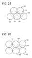
- the transparent spherical members may be positioned at respective vertices of a triangle or a rectangle, as shown in Fig. 25 or Fig. 26, respectively, and respective positions of the photovoltaic elements are determined by the respective positions of the spherical members.
- each photovoltaic element is supported by three spherical members; and, in the example shown in Fig. 26, each photovoltaic element is supported by four spherical members.
- the photovoltaic panel (i.e., closest packing) shown in Fig. 25 in which each photovoltaic element is supported by three spherical members enjoys a higher density of photovoltaic elements than that shown in Fig. 26.
- respective positions of the photovoltaic elements are determined by the spherical members. That is, the photovoltaic elements can be positioned at respective desirable positions by selecting the size of the spherical members or the pattern in which the spherical members are positioned.
- the spherical members are formed of an optical ceramics or an optical resin.
- the spherical members have a higher strength than the photovoltaic elements, but this feature is not essentially needed.
- the photovoltaic-element holding member may be produced by first using the spherical members to hold the photovoltaic elements, casting a material before curing,a and then curing the material.
- the material before curing has a lower viscosity than that of the light-transmitting material.
- the temporarily-holding member is formed of an elastic material, and wherein the step of temporarily holding comprises stretching the temporarily-holding member holding the photovoltaic elements, to change a space between each pair of adjacent photovoltaic elements of the plurality of photovoltaic elements.
- the space between each pair of photovoltaic elements adjacent to each other can be increased by stretching the temporarily holding member.
- An amount of increasing of the space can be changed by changing an amount or proportion of stretching of the temporarily holding member.
- the temporarily holding member holds the photovoltaic elements such that there remains substantially no space between each pair of adjacent photovoltaic elements
- a space is produced between each pair of adjacent photovoltaic elements, by stretching the temporarily holding member.
- arranging the photovoltaic elements such that there remains substantially no space between each pair of adjacent photovoltaic elements is easier than arranging the elements such that there remains a predetermined space between each pair of adjacent elements, and the photovoltaic elements arranged in the former manner enjoys a higher density than those arranged in the latter manner.
- the temporarily holding member can be stretched in one direction only, or in each of two directions that intersect each other, preferably, two directions that are perpendicular to each other.
- the present invention provides a photovoltaic panel comprising:
- This aspect of the present invention also provides a photovoltaic panel, comprising:
- a preferred embodiment provides a photovoltaic panel, comprising:
- both the first and second electrodes are formed on one of opposite sides of a first plane that intersects the photovoltaic elements, and the light-transmitting layer is formed on the other side of the plane.
- the light-transmitting layer is formed of a light-transmitting material which fills a space between the first plane and a second plane which is tangent to the photovoltaic elements.
- the material used to form the light-transmitting layer may be an optical ceramics or an optical resin.
- the material is excellent with respect to light transmittance and is free of yellowing. More preferably, the material is excellent with respect to weather resistance, chemical resistance, and electrical insulation, and has a mechanical strength higher than a certain degree. More preferably, the material is excellent with respect to moldability or formability.
- the material may be toughened glass, acrylic resin, urethane resin, polycarbonate resin, or unsaturated-polyester resin.
- the light-transmitting layer may be called as a photovoltaic-element holding layer.
- the first plane divides each of the photovoltaic elements into a first portion whose volume is smaller than 50 % of a volume of the each photovoltaic element, and a second portion whose volume is greater than 50 % of the volume, and wherein the light-transmitting layer is provided on the other side of the first plane on which the respective second portions of the photovoltaic elements are located.
- Electric power is generated at the P-N junction of each photovoltaic element.
- each photovoltaic element has a generally spherical shape and somewhat more than 50% of the each element is embedded in the light-transmitting layer, at least half the each element can be utilized to generate electric power, irrespective of which side of the photovoltaic panel the light may be incident to.
- each photovoltaic element it is required that some portion of each photovoltaic element remain not embedded in the light-transmitting layer. In view of this, it is preferred that not more than 60%, 65%, 70%, 75%, or 80% of each photovoltaic element be embedded in the layer.
- the light-transmitting layer has a shape having two plane surfaces parallel to each other, and wherein one of the two plane surfaces is substantially parallel to the first plane and the other plane surface is substantially parallel to the second plane.
- the photovoltaic panel can be used with ease.
- the light receiving surface may be provided by a plane surface, the light is prevented from being scattered by the light receiving surface.
- an angle of incidence of the light to the photovoltaic panel can be easily changed.
- the present invention also provides a method of producing a photovoltaic panel, comprising the steps of:
- the light-transmitting layer is formed of a light-transmitting material before curing, and respective portions of the photovoltaic elements are embedded in the light-transmitting layer. Then, the light-transmitting layer is cured to produce a photovoltaic-element holding member.
- the present method can more easily produce the photovoltaic-element holding member than the conventional method in which, after a light-transmitting resin is applied to photovoltaic elements, the resin is cured.
- the light-transmitting layer before curing has physical properties which allow respective portions of the photovoltaic elements to be embedded therein, that is, properties which maintain a state in which respective portions of the photovoltaic elements are embedded therein. It can also be said that the light-transmitting layer before curing has physical properties which assure that the layer is deformed while keeping close contact with the photovoltaic elements. Because of the physical properties of the light-transmitting layer, the layer behaves like a fluid (i.e., is deformed) and respective portions of the photovoltaic elements can be embedded in the layer. In many cases, the light-transmitting layer is in a half-solid (or gel) state, but in some cases, it is in a liquid state. That the light-transmitting layer is in a state in which the photovoltaic elements can be embedded therein may be expressed in terms of a viscosity, or an elasticity, of the light-transmitting layer.
- the light-transmitting layer needs to have physical properties which assure that respective portions of the photovoltaic elements are embedded therein, just at the time when the embedding step is carried out.
- the layer may have other physical properties.
- the layer which has just been formed may have so low a viscosity that the layer cannot maintain a state in which respective portions of the photovoltaic elements are embedded therein.
- the layer When the light-transmitting layer is cured in a state in which respective portions of the photovoltaic elements are embedded therein, the layer can hold the photovoltaic elements. If at least respective portions of the photovoltaic elements are embedded in the layer, the layer can hold the elements.
- the step of embedding comprises embedding more than 50 % of a volume of each of the photovoltaic elements, in the light- transmitting layer.
- the step of embedding comprises embedding more than 50 % of an area of junction of a P-type layer and an N-type layer of each of the photovoltaic elements, in the light-transmitting layer.
- the step of embedding comprises embedding, in the light-transmitting layer, the photovoltaic elements such that an electric-power generating efficiency per unit area of the photovoltaic panel is higher than a predetermined value.
- Electric power is generated at the P-N junction of each photovoltaic element.
- each photovoltaic element may be shaded by another portion of the same.
- electric power is generated by light incident through the light-transmitting layer and each photovoltaic element has a generally spherical shape, it is preferred that somewhat more than 50% of the each element be embedded in the light-transmitting layer.
- the step of curing comprises at least one of heating the light-transmitting layer, cooling the light-transmitting layer, and exposing the light-transmitting layer to light.
- the material used to form the light-transmitting layer is cured after the photovoltaic elements are embedded therein. Some materials are heated for curing; some materials are cooled for curing; and other materials are exposed to light, such as ultraviolet rays or light containing ultraviolet rays, for curing.
- the materials that are cured by heating are, e.g.., thermosetting resins; the materials that are cured by cooling are, e.g., glass; and the materials that are cured by light are, e.g., photocurable resins (or photosensitive resins).
- the material be excellent with respect to not only light transmittance but also heat resistance and weather resistance.
- thermosetting resins are, e.g., UV-curable acrylic resins or UV-curable urethane resins.
- the step of embedding comprises:
- the temporarily holding surface of the temporarily holding member holds a number of photovoltaic elements
- the temporarily-holding member holding the photovoltaic elements is moved toward the light-transmitting layer, so that respective portions of the photovoltaic elements are embedded in the light-transmitting layer. That is, the photovoltaic elements are embedded in the light-transmitting layer, not directly, but indirectly using the temporarily-holding member.
- the photovoltaic elements can be more easily embedded in the light-transmitting layer before curing, if the elements are temporarily held by the temporarily holding surface of the temporarily holding member, than if the elements are directly embedded at respective predetermined positions (or in a predetermined pattern) in the light-transmitting layer.
- the temporarily holding member is provided by a flat member, the member can be easily operated. However, it is not essentially required that the temporarily holding member be provided by a flat member. Similarly, the temporarily holding surface may be either a plane surface or a curved surface.
- the temporarily holding member is preferably formed of a light-transmitting material.
- the temporarily holding member is preferably formed of a material which is excellent to heat transfer. In many cases, the light-transmitting layer can be more easily cured or set by heat applied, or light incident, to the temporarily holding member.
- the step of temporarily holding comprises temporarily fixing the photovoltaic elements to an adhesive layer which is formed on the temporarily holding surface of the temporarily holding member.
- the adhesive layer needs to hold just temporarily the photovoltaic elements, and need not hold the same for a long time.
- the adhesive layer is, e.g., a transparent adhesive sheet.
- the step of temporarily holding comprises temporarily holding, with an arranging member, the photovoltaic elements on the temporarily holding surface of the temporarily holding member.
- the photovoltaic elements can be positioned at respective desired positions on the temporarily holding surface of the temporarily holding member.
- the arranging member may be used to define a distance between each pair of photovoltaic elements adjacent to each other.
- the arranging member may be one which has a number of openings.
- the temporarily-holding member is formed of an elastic material, and wherein the step of temporarily holding comprises stretching the temporarily-holding member holding the photovoltaic elements, to change a space between each pair of adjacent photovoltaic elements of the plurality of photovoltaic elements.
- the space between each pair of photovoltaic elements adjacent to each other can be increased by stretching the temporarily holding member.
- An amount of increasing of the space can be changed by changing an amount or proportion of stretching of the temporarily holding member.
- the temporarily holding member holds the photovoltaic elements such that there remains substantially no space between each pair of adjacent photovoltaic elements
- a space is produced between each pair of adjacent photovoltaic elements, by stretching the temporarily holding member.
- arranging the photovoltaic elements such that there remains substantially no space between each pair of adjacent photovoltaic elements is easier than arranging the elements such that there remains a predetermined space between each pair of adjacent elements, and the photovoltaic elements arranged in the former manner enjoys a higher density than those arranged in the latter manner.
- the temporarily holding member may be stretched in one direction only, or in each of two directions that intersect each other, preferably, two directions that are perpendicular to each other.
- the step of moving the temporarily-holding member comprises moving the temporarily-holding member toward the light-transmitting layer, while preventing contraction of the temporarily-holding member stretched.
- the temporarily-holding member is provided by an elastic member which is not plastically deformed when being stretched by an external force, i.e., which is used within a range of elastic deformation
- the temporarily-holding member contracts because of its elastic force, if the external force is removed.
- the temporarily-holding member is kept stretched to prevent its contraction.
- the step of temporarily holding comprises:
- the spaces among the photovoltaic elements can be reduced and can be easily packed such that there is substantially no space between each pair of adjacent photovoltaic elements.
- the density of the photovoltaic elements held by the temporarily holding member can be easily increased.
- the step of moving comprises pressing, in a state in which the photovoltaic elements contact the light-transmitting layer, the temporarily-holding member and the light-transmitting layer against each other.
- the photovoltaic elements can be easily forced into the light-transmitting layer.
- a stopper which defines a limit of movement of the temporarily-holding member and the light-transmitting layer toward each other. In the latter case, it is possible to embed appropriately the photovoltaic elements in the light- transmitting layer.
- the photovoltaic elements can be embedded in the light-transmitting layer being cured.
- the step of producing further comprises removing, after the step of curing, the temporarily holding member from the light-transmitting layer cured.
- the temporarily-holding member is removed from the layer to provide the photovoltaic-element holding member.
- the step of forming the light-transmitting layer comprises supplying the light-transmitting material to a container and thereby forming the light-transmitting layer.
- the light-transmitting layer is formed of a material in a liquid or half-solid state. Accordingly, the light-transmitting layer can be easily formed using the container.
- the container is used for just forming the light-transmitting layer and is not used as part of the photovoltaic panel. Therefore, after the photovoltaic-element holding member is produced, or after the photovoltaic panel is produced, the container is removed.
- the container may be employed as part of the photovoltaic panel.
- the container In the case where at least a portion of the container is formed of a light-transmitting material, that portion of the container need not be removed. That is, that portion of the container can be deemed as part of the light-transmitting layer, and a rigidity of the photovoltaic panel can be increased by that portion of the container.
- the container can be used to protect the light-transmitting layer during the production of the photovoltaic panel.
- a portion of the container may be utilized as a stopper which defines a limit of movement of the temporarily holding member toward the container.
- the container is not essentially needed to form the light-transmitting layer.
- the light-transmitting layer is formed of a material having a high viscosity, the container is not needed.
- the step of forming the at least one electrode comprises forming two electrodes on one of opposite sides of the photovoltaic-element holding member.
- the step of forming the at least one electrode may comprise forming two electrodes on opposite sides of the photovoltaic-element holding member, respectively.
- An electrode connected to respective P-type layers of the photovoltaic elements, and an electrode connected to respective N-type layers of the elements may be both provided on one of opposite sides of the photovoltaic-element holding member, or may be respectively provided on the opposite sides of the holding member.
- one electrode which is provided on one side of the holding member to which light is incident is formed to cover only a portion of the light receiving surface of the holding member so that the light is efficiently utilized by the photovoltaic elements, or is formed of a transparent material.
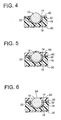
- reference numeral 10 designates a silicon ball as a photovoltaic element.
- the silicon ball 10 includes a core portion or layer 12 as a P-type silicon, and a shell portion or layer 14 as an N-type silicon.
- Reference numeral 16 denotes a holding plate as a light-transmitting layer that holds a number of silicon balls or photovoltaic elements 10.
- a number of recesses 18 each as a photovoltaic-element holding portion are formed in a photovoltaic-element holding surface 17 of the holding plate 16, such that the recesses 18 are distant from one another at predetermined regular intervals (this is a photovoltaic-element-holding-portion forming step), and a photovoltaic element 10 is placed in each of the recesses 18.
- Each of the recesses 18 is provided with adhesive, and a photovoltaic element 10 is fixed to the each recess 18 via an adhesive layer 20 (this is a photovoltaic-element-holding-member producing step or a photovoltaic-element fixing step).
- the photovoltaic elements 10 and the holding plate 16 cooperate with each other to provide a photovoltaic-element holding plate 22 as a photovoltaic-element holding member.
- the holding plate 16 be formed of a material which is excellent with respect to light transmittance, chemical resistance, weather resistance, electrical insulation, and adhesiveness to silicon, and has a certain degree of mechanical strength.
- the holding plate 16 is formed of a material which is free of yellowing.
- the holding plate 16 is formed of an optical ceramics, such as toughened glass, or an optical resin, such as acrylic resin, urethane resin, or polycarbonate resin.
- the intervals between the recesses 18 of the holding plate 16 are so optimized as to locate appropriately the photovoltaic elements 10. If the intervals are too small, a power generating efficiency of each photovoltaic element 10 lowers; and if the intervals are too great, i.e., if the density of the photovoltaic elements 10 is too low, a power which is generated by each photovoltaic panel lowers.
- the intervals between the photovoltaic elements 10, i.e., respective positions of the recesses 18 are determined based on, e.g., a size of the elements 10.
- the photovoltaic elements 10 are located at the respective positions on the holding plate 16 where the recesses 18 are formed, and accordingly the holding plate 16 functions as an arranging plate. In addition, as will be described later, the photovoltaic elements 10 receive light via the holding plate 16. Thus, the holding plate 16 also functions as a light receiving plate or a light-incident plate.
- the adhesive (i.e., resin) used to form the adhesive layer 20 may be one which has the same properties as those of the holding plate 16 (the adhesive may be the same material as that of the holding plate 16). However, the adhesive does not need a high degree of mechanical strength. Thus, it is preferred that the adhesive be excellent with respect to at least light transmittance, adhesiveness to the photovoltaic elements 10 (silicon), and adhesiveness to the holding plate 16. In addition, preferably, the adhesive is excellent with respect to applicability to the holding plate 16, i.e., semi-solid (gel) or liquid in use. Moreover, the adhesive is desired to contain a thermosetting resin or a photocurable resin.
- the adhesive is heated, or exposed to light, to fix the elements 10 to the holding plate 16.
- the adhesive may be one which contains an acrylic resin, a urethane resin, a polycarbonate resin, or an unsaturated-polyester resin.
- the photovoltaic elements 10 At any rate, it is not needed to position, with high accuracy, the photovoltaic elements 10 relative to the holding plate 16 or produce the elements 10 themselves with highly accurate dimensions. That is, it is not needed to produce, with high accuracy, the photovoltaic-element holding plate 22, and as such the cost of production of the plate 22 can be lowered.
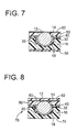
- a protective layer 30 is formed on an opposite surface of the holding plate 16 that is opposite to the holding surface 17 (this is a protective-layer forming step), and subsequently a first electrode portion 32 is so formed as to cover the holding surface 17 of the photovoltaic-element holding plate 22 and respective projecting portions of the photovoltaic elements 10 that project from the holding plate 16 (this is an electrode-plate forming step).
- the protective layer 30 is provided for preventing a plating liquid from adhering to the holding plate 16, or preventing the holding plate 16 from being mechanically damaged. That is, the protective layer 30 is provided for preventing lowering of the light transmittance of the holding plate 16.
- a commercially available masking tape (for example, a solder-adhesion preventing tape which can be called as solder masking tape) may be used as the protective layer 30. The masking tape can be easily peeled while leaving little glues.
- the first electrode portion 32 is formed by a chemical plating (electroless plating) using a plating liquid containing a nickel alloy.
- a nickel coating electrically conductive layer
- the conductive layer may be formed of a different material than the nickel alloy; for example, aluminum, cobalt, palladium, copper, silver, gold, or any alloy containing al least one of those metals.
- the conductive layer may be formed by a different method than the chemical plating; for example, CVD (chemical vapor deposition), PVD (physical vapor deposition), or direct application of a conductive material (e.g., conductive silver paste adhesive).
- the first electrode portion 32 may be provided by not a single conductive layer but a plurality of conductive layers (metallic layers) that are stacked on each other. In the latter case, the electrical conductivity can be stabilized. In the latter case, the plurality of conductive layers may be formed by a same sort of metal, or different sorts of metals.
- an electrically insulating layer 40 is formed on portions of the first electrode portion 32 that correspond to the holding surface 17 of the holding plate 16 (this is an insulating-layer forming step).
- the insulating layer 40 needs to be formed of an electrically insulting material, but need not be formed of a light-transmitting material.
- the insulting layer 40 may be formed of an acrylic resin, a urethane resin, a polycarbonate resin, an unsaturated-polyester resin, or an epoxy resin.
- the insulating layer 40 may be formed by first applying, using a brush, the resin in gel or liquid and then irradiating or heating the resin.
- the insulating layer 40 may include portions that are formed on portions of the first electrode portion 32 that correspond to the photovoltaic elements 10. However, those portions of the insulating layer 40 are removed together with those portions of the first electrode portion 32, in the subsequent removing step.
- the insulating layer 40 may be formed in such a manner that a film having openings at respective positions corresponding to the recesses 18 of the holding plate 16 is placed on the first electrode portion 32 of the photovoltaic-element holding plate 22, such that the openings are aligned with the photovoltaic elements 10, and subsequently the film is heated, or heated and pressed, to form the layer 40 (this is a heat- or pressure-utilizing insulating-layer forming step).
- the film is a flexible or transparent one, the insulating layer 40 can be easily formed of the film.
- the above-indicated portions of the first electrode portion 32 and the above-indicated portions of the insulating layer 40 are mechanically removed by sand blasting (this is an insulating-layer removing step and a first-electrode-portion removing step). Then, a portion of the N-type shell layer 14 of each photovoltaic element 10 is removed by etching to expose the P-type core layer 12 (this is an N-type-layer removing step).
- a mixture of hydrofluoric acid (HF) and nitric acid (HNO 3 ) may be used as an etching liquid.
- another electrically insulating layer 50 is formed, in the same manner as described above, on the side of the holding surface 17 of the photovoltaic-element holding plate 22 (this is an insulating-layer forming step).
- the insulating layer 50 covers the respective N-type layers 14 of the photovoltaic elements 10 and the first electrode portion 32.
- the insulating layer 50 may be formed of the same material as that of the insulating layer 40.
- the insulating layer 50 need not be formed of a light-transmitting material.
- a photovoltaic panel as a whole can be formed to have a flat shape, and accordingly can be used with each.
- a second electrode portion 60 can be formed easily.
- the insulating layer 50 is formed except on the respective P-type layers 12 of the photovoltaic elements 10, it is not needed to remove any portions of the insulating layer 50. In addition, it is not essential to form the respective flat portions 54 of the P-type layers 12.
- the second electrode portion 60 is formed (this is a second-electrode-portion forming step).
- the second electrode portion 60 is so formed as to cover all the respective flat portions 54 of the photovoltaic elements 10 and the entirety of the insulating layer 50.
- the second electrode portion 60 may be formed of the same material as that of the first electrode portion 30, in the same manner as that in which the first electrode 30 is formed.
- a protective layer 62 is formed to protect the second electrode portion 60 (this is a protective-layer forming step).
- the protective layer 62 may be formed of ceramics, metal, or resin (e.g., toughened plastics).
- the protective layer 30 is removed to provide a photovoltaic panel 70 having a light-receiving surface 72 thus exposed.
- both the first and second electrode portions 32, 60 are formed on one of opposite sides of the photovoltaic-element holding plate 22, and neither of them are formed on the other side. Therefore, the area of the light-receiving surface 72 is not decreased by the provision of those electrode portions 32, 60, and the light incident to the surface 72 can be most efficiently utilized.
- the photovoltaic-element holding plate 22 may be formed in a different manner than the above-described manner.
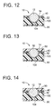
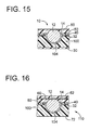
- Fig. 9 shows another embodiment in which a holding plate 100 has, in a holding surface 102 thereof, a number of photovoltaic-element holding portions 104 each of which has a shape corresponding to the shape of each photovoltaic element 10.
- a pressure force or a pressure is applied to the photovoltaic elements 10 to force the elements 10 into the photovoltaic-element holding portions 104, and thereby form a photovoltaic-element holding member 106.
- Figs. 9, 10, 11, 12, 13, 14, and 15 show respective steps of a method in which a photovoltaic panel 110 is produced using the photovoltaic- element holding member 106, and Fig. 16 shows the photovoltaic panel 110 thus produced.
- each photovoltaic-element holding portion 104 be somewhat smaller than a size of each photovoltaic element 10. In this case, each element 10 can be surely fitted in, and fixed to, the holding plate 100. However, the photovoltaic elements 10 may be fixed to the holding plate 100 with an adhesive, like in the preceding embodiment.
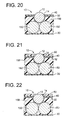
- Fig. 17 shows another embodiment in which a photovoltaic-element holding member is formed using generally spherical holding members 150. More specifically described, the spherical holding members 150, each having a uniform size somewhat larger than each photovoltaic element 10, are arranged into a single, closest-packed layer (this is a spherical-holding-portion arranging step). Then, photovoltaic elements 10 are supplied onto the layer of spherical holding members 150, and additionally a gel or half-solid material is supplied (this is a photovoltaic-element supplying step). The gel or half-solid material is cured and a photovoltaic-element holding member 152 is formed. In the present embodiment, the gel or half-solid material is cured into a light-transmitting adhesive layer 156.
- Each of the spherical holding members 150 is formed of a light-transmitting material, which may be plastics, ceramics (e.g., glass), or metal. It is preferred that the adhesive layer 156 be formed of a light-transmitting material which can be well adhered to both the spherical holding members 150 and the photovoltaic elements 10. In the case where the spherical holding members 150 and the adhesive layer 156 are formed of a same material, a difference between refraction factors of the members 150 and the layer 156 can be minimized to advantage.
- the spherical holding members 150 are arranged such that every three adjacent members 150 define a triangle (in a closest-packed state), and each photovoltaic element 10 is positioned at the center of the triangle.
- the positioning of each photovoltaic element 10 depends on the state in which the spherical holding members 150 are packed.
- Figs. 17, 18, 19, 20, 21, 22, and 23 show respective steps of a method in which a photovoltaic panel 160 is produced using the photovoltaic-element- holding member 152, and Fig. 24 shows the photovoltaic panel 160 thus produced.
- the photovoltaic elements 10 can be arranged with ease, without needing to position, with accuracy, the individual elements 10 at respective predetermined positions.
- the spherical holding members 150 may be arranged in not the state shown in Fig. 25 but a state shown in Fig. 26. More specifically described, the spherical holding members 150 are arranged such that every four adjacent members 150 define a square, and each photovoltaic element 10 is positioned at the center of the square. When the photovoltaic elements 10 positioned at the respective centers of the squares are compared with the photovoltaic elements 10 positioned at the respective centers of the triangles, the latter elements 10 enjoys a higher density and generates more electric power per area of photovoltaic panel, than the former elements 10.
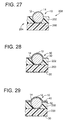
- Fig. 27 shows another embodiment in which two layers are provided to hold photovoltaic elements 10.
- a resin layer 202 is formed of a light-transmitting material that is in gel in use before curing (this is a holding-layer forming step). Then, the photovoltaic elements 10 are partly embedded (this is an embedding step), and subsequently the resin layer 202 is cured (this is a curing step) to hold firmly the elements 10.
- the flat member 200 and the resin layer 202 cooperate with each other to provide a holding layer 204 as a light-transmitting layer, and the holding layer 204 and the photovoltaic elements 10 cooperate with each other to provide a photovoltaic-element holding member 206.
- the photovoltaic elements 10 are embedded in the resin layer 202 before curing. Thus, it is not needed to form, in the holding layer 204, any photovoltaic-element holding portions such as recesses.
- the resin layer 202 may be formed of a material which does not have a mechanical rigidity. Thus, the degree of freedom of choice of material is increased.
- the photovoltaic elements 10 can be accurately embedded in the resin layer 202, without needing to adjust the amount of embedding, because the embedding of the elements 10 is stopped by the rigid flat member 200.
- Figs. 27, 28, 29, 30, 31, 32, and 33 show respective steps of a method in which a photovoltaic panel 210 is produced using the photovoltaic-element holding member 206, and Fig. 34 shows the photovoltaic panel 210 thus produced.
- the flat member 200 may be omitted, and the holding layer as the light-transmitting layer may be provided by the resin layer 202 only.
- the photovoltaic elements 10 are directly embedded in the resin layer 202 in gel, to produce the photovoltaic-element holding member 206.
- the photovoltaic elements 10 may be embedded using a temporarily holding member.
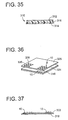
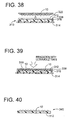
- Figs 35, 36, 37, 38, 39, 40, and 41 show respective steps of a method in which a photovoltaic-element holding member is produced using the temporarily holding member.
- the method will be described.
- a resin is supplied into a container 310 to form a light-transmitting layer 312 (this is a light-transmitting-layer forming step).
- the container 310 includes a bottom portion 314 and a frame portion 316, and the bottom portion 314 is formed of polycarbonate.
- the resin supplied to the container 310 is in a state before curing, e.g., in a gel (or half-solid) state in the present embodiment.
- the resin need not be in the gel state when the resin is supplied to the container 310, but may be in a liquid state.
- photovoltaic elements 10 are embedded in the resin, the resin needs to be in the gel (or half-solid) state.
- the light-transmitting layer 312 be formed of a material which is excellent with respect to light transmittance, weather resistance, electric insulation, chemical resistance, and heat resistance and is free of yellowing.
- the layer 312 is formed of a material which is excellent with respect to formability.
- the layer 312 is preferably formed of a thermosetting resin, or a photocurable resin such as a resin which is cured by light such as ultraviolet rays. Since the container 310 is removed as described later, the container 310 need not be formed of a light-transmitting material.
- the photovoltaic elements 10 are temporarily held by a temporarily-holding plate 318 as a temporarily-holding member (this is a temporarily holding step). More specifically described, an adhesive is applied to a flat, temporarily-holding surface 322 of the temporarily-holding plate 318, so as to form an adhesive layer 324, and the photovoltaic elements 10 are temporarily held by the temporarily-holding plate 318, with the help of an arranging plate 326. Thus, the photovoltaic elements 10 are temporarily held by the adhesive layer 324.
- the temporarily-holding plate 318 is formed of a glass plate and accordingly can transmit light. Since the light-transmitting layer 312 in the gel state is formed of a photocurable material which is cured by light such as ultraviolet rays, the layer 312 is irradiated with ultraviolet rays, or light containing ultraviolet rays, through the temporarily-holding plate 318. In the case where the container 310 is formed of a light-transmitting material, the layer 312 may be irradiated through the container 310. However, it is easier to irradiate the layer 312 through the plate 318, than through the container 310.
- the temporarily-holding plate 318 be formed of a material which is excellent with respect to heat transfer, so that heat can be effectively transferred to the layer 312 via the plate 318.
- the temporarily-holding plate 318 need not be able to transmit light.
- the temporarily-holding surface 322 of the temporarily-holding plate 318 need not be flat but may be curved.
- the temporarily-holding surface 322 may have a shape corresponding to that of a photovoltaic panel.
- the adhesive used to form the adhesive layer 324 be one whose degree of adhesiveness to the photovoltaic elements 10 is lower than that of the light-transmitting layer 312. Thus, when the temporarily-holding plate 318 is removed, the photovoltaic elements 10 are prevented from coming off the light-transmitting layer 312, as will be described later.
- the arranging plate 326 has a number of openings 336, as shown in Fig. 36, and the photovoltaic elements 10 fall, through the openings 336, onto respective predetermined positions on the adhesive layer 324 (or the temporarily-holding surface 322), and are temporarily adhered and held thereon.
- the temporarily-holding plate 318 is moved toward, and pressed against, the light-transmitting layer 312 till about one half of each of the photovoltaic elements 10 is embedded in the layer 312 (this is a moving step or a pressing step).
- the light-transmitting layer 312 is irradiated with ultraviolet rays, or light containing ultraviolet rays, through the temporarily-holding plate 318, so that the layer 312 is cured (this is a curing step).
- the temporarily-holding plate 318 is moved, under pressure, toward the light-transmitting layer 312 till the temporarily-holding surface 322 thereof contacts an end surface 338 of the framework 316 of the container 310.
- a holding surface 339 of the light-transmitting layer 312 present in the container 310 is somewhat lower than the end surface 338 of the framework 316.
- the end surface 338 functions as a stopper which defines a limit of movement of the plate 318 toward the container 310.
- an amount of embedding of each photovoltaic element 10 in the layer 312 can be changed by changing a height position of the holding surface 339 relative to the end surface 338.
- each photovoltaic element 10 has a generally spherical shape
- about a half of each element 10 can be utilized to generate electric power, irrespective of whether the element 10 is irradiated with light through the light-transmitting layer 312, or not through the same 312.
- the each element 10 is firmly held by the layer 312.
- the container 310 is removed after the photovoltaic-element holding plate 340 is produced.
- the container 310 may be removed after a photovoltaic panel is produced.
- the container 310 is used as a protective member which protects the light-transmitting layer 312.
- the container 31.0 can prevent metal from adhering to the layer 312, e.g., when electrode portions are formed, or prevent the layer 312 from being mechanically damaged during the producing steps.
- the bottom portion 314 and the frame portion 316 of the container 310 may, or may not, be ones which transmit light. If those portions 314, 316 transmit light, those portions 314, 316 can be deemed as part of the light-transmitting layer 312 and need not be removed. In the latter case, a rigidity of the layer 312 is increased as such, and accordingly respective rigidities of the photovoltaic-element holding plate 340 and the photovoltaic panel are increased.
- a photovoltaic-element holding plate is produced in a different method than the above-described method.
- the photovoltaic elements 10 are temporarily held, with the help of the arranging plate 326, by the adhesive layer 324 of the temporarily-holding plate 318, and those elements 10 are embedded in the light-transmitting layer 312 before curing, to produce the photovoltaic-element holding plate 340.
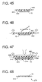
- a high density of photovoltaic elements 10 are temporarily held on an adhesive layer 454 provided on a temporarily-holding surface 452 of a temporarily-holding plate 450 which is formed of an elastic material such as rubber.
- the temporarily-holding plate 450 is elastically stretched in two directions perpendicular to each other, so as to produce respective appropriate spaces among the photovoltaic elements 10.
- the photovoltaic elements 10 are embedded in the light-transmitting layer 312, to produce a photovoltaic-element holding plate 458.
- the photovoltaic elements 10 are supplied into a container 464 including a bottom portion 460 and a side portion 462.
- a container 464 including a bottom portion 460 and a side portion 462.
- the adhesive layer 454 is formed on the temporarily-holding surface 452 of the temporarily-holding plate 450. As shown in Figs. 44 and 45, the adhesive layer 454 is pressed against the photovoltaic elements 10 arranged in the container 464, for example, using a pressing member 472. Since the temporarily-holding surface 452 of the temporarily-holding plate 450 contacts an upper surface of the side portion 462 of the container 464, the photoelectric elements 10 are prevented from receiving an excessively great force.
- the temporarily-holding plate 450 is stretched, by a biaxial stretching machine, not shown, in two directions perpendicular to each other. Since the plate 450 is formed of an elastic material, the plate 450 can be stretched with a considerably small force, so as to produce respective appropriate spaces among the photovoltaic elements 10. The spaces produced among the elements 10 can be changed by changing an amount of the stretching by the stretching machine.
- the temporarily-holding plate 450 is maintained in the stretched state.
- the plate 450 is prevented from contracting, if a frame member is fitted in an outer peripheral portion of the plate 450 being stretched by the biaxial stretching machine.
- the temporarily-holding plate 450 is moved toward the light-transmitting layer 312, like in the above-described method, so that the photovoltaic elements 10 are embedded in the layer 312.
- the layer 312 is irradiated with ultraviolet rays, or light containing ultraviolet rays, so as to produce the photovoltaic-element holding plate 458.
- Fig. 47 shows that the light-transmitting layer 312 is irradiated with ultraviolet light that is incident from the side of the pressing member 480. However, if the pressing member 480 cannot transmit much light, the layer 312 may be irradiated with ultraviolet light that is incident from the side of the container 464.
- the spaces among the photovoltaic elements 10, i.e., the respective positions of the elements 10 can be arbitrarily changed by changing the amount of stretching of the temporarily-holding plate 450.
- the density of the photovoltaic elements 10 held by the plate 450 can be adjusted.
- the density of the elements 10 can be increased, and accordingly the power-generating efficiency of the elements 10 can be increased.
- the photovoltaic elements 10 may not have a uniform shape.
- the density of the elements 10 of the photovoltaic-element holding member 458 can be increased even if the elements 10 may not have a uniform shape or size.
- the temporarily-holding plate 450 is stretched in the two directions perpendicular to each other.
- a resin is supplied into a container 510 to form a light-transmitting layer 512 (this is a light-transmitting-layer forming step).
- the container 510 includes a bottom portion 514 and a frame portion 516, and the bottom portion 514 is formed of polycarbonate.
- the resin supplied to the container 510 is in a state before curing, e.g., in a gel (or half-solid) state in the present embodiment.
- the resin need not be in the gel state when the resin is supplied to the container 510, but may be in a liquid state.
- photovoltaic elements 520 are embedded in the resin, the resin needs to be in the gel (or half-solid) state.
- the light-transmitting layer 512 be formed of a material which is excellent with respect to light transmittance, weather resistance, electric insulation, chemical resistance, and heat resistance and is free of yellowing.
- the layer 312 is formed of a material which is excellent with respect to formability.
- the layer 512 is preferably formed of a thermosetting resin, or a photocurable resin such as a resin which is cured by light such as ultraviolet rays. Since the container 510 is removed as will be described later, the container 510 need not be formed of a light-transmitting material.
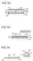
- the photovoltaic elements 520 are temporarily held by a temporarily-holding plate 518 as a temporarily-holding member (this is a temporarily holding step). More specifically described, an adhesive is applied to a flat, temporarily-holding surface 522 of the temporarily-holding plate 518, so as to form an adhesive layer 524, and the photovoltaic elements 520 are temporarily held by the temporarily-holding plate 518, with the help of an arranging plate 526. Thus, the photovoltaic elements 520 are temporarily held by the adhesive layer 524.
- each of the photovoltaic elements 520 has a generally spherical shape, and includes a core portion 532 as a P-type layer, and a shell portion 534 as an N-type layer.
- the N-type layer 534 is formed by doping of the shell portion of a P-type silicon ball.
- each photovoltaic element 520 may not be a spherical one.
- the temporarily-holding plate 518 is formed of a glass plate and accordingly can transmit light. Since the light-transmitting layer 512 in the gel state is formed of a photocurable material which is cured by light such as ultraviolet rays, the layer 512 is irradiated with ultraviolet rays, or light containing ultraviolet rays, through the temporarily-holding plate 518. In the case where the container 510 is formed of a light-transmitting material, the layer 512 may be irradiated through the container 510. However, it is easier to irradiate the layer 512 through the plate 518, than through the container 510.
- the temporarily-holding plate 518 be formed of a material which is excellent with respect to heat transfer, so that heat can be effectively transferred to the layer 512 via the plate 518.
- the temporarily-holding plate 518 need not be able to transmit light.
- the temporarily-holding surface 522 of the temporarily-holding plate 518 need not be flat or plane, but may be curved. That is, the temporarily-holding surface 522 (i.e., the shape of the temporarily-holding plate 518) can have a shape corresponding to that of a photovoltaic panel as an end product.
- the adhesive used to form the adhesive layer 524 is one whose degree of adhesiveness to the photovoltaic elements 520 is lower than that of the light-transmitting layer 512. Thus, when the temporarily-holding plate 518 is removed, the photovoltaic elements 10 are prevented from coming off the light-transmitting layer 512, as will be described later.
- the arranging plate 526 has a number of openings 536, as shown in Fig. 50, and the photovoltaic elements 520 fall, through the openings 536, onto respective predetermined positions on the adhesive layer 524 (or the temporarily-holding surface 522), and are temporarily adhered and held thereon.
- the temporarily-holding plate 518 is moved toward, and pressed against, the light-transmitting layer 512 till about one half of each of the photovoltaic elements 520 is embedded in the layer 512 (this is a moving step or a pressing step).
- the light-transmitting layer 512 is irradiated with ultraviolet rays, or light containing ultraviolet rays, through the temporarily-holding plate 518, so that the layer 512 is cured (this is a curing step).
- the temporarily-holding plate 518 is moved, under pressure, toward the light-transmitting layer 512 till the temporarily-holding surface 522 thereof contacts an end surface 538 of the framework 516 of the container 510.
- a holding surface 539 of the light-transmitting layer 512 present in the container 510 is somewhat lower than the end surface 538 of the framework 516.
- the end surface 538 functions as a stopper which defines a limit of movement of the plate 518 toward the container 510.
- an amount or proportion of embedding of each photovoltaic element 520 in the layer 512 can be changed by changing a height position of the holding surface 539 relative to the end surface 538.
- each photovoltaic element 520 has a generally spherical shape
- about a half of each element 520 can be utilized to generate electric power, irrespective of whether the each element 10 is irradiated with light through the light-transmitting layer 512, or not through the same 512.
- the each element 520 is firmly held by the layer 512.
- both a P-type-layer electrode portion and an N-type-layer electrode portion are formed on one of opposite sides of the photovoltaic-element holding plate 540.
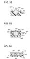
- the N-type-layer electrode portion 550 is formed on the one side of the photovoltaic-element holding plate 540 on which the photovoltaic elements 520 project (this is an N-type-layer forming step).
- the N-type-layer electrode portion 550 is formed by vapor deposition of an electrically conductive material such as aluminum, titan, or an alloy containing one or both of those metals.
- a protective layer 552 is formed to protect the N-type-layer electrode portion 550 (this is a protective-layer forming step).
- the protective layer 552 may be either electrically insulating or conductive.
- the protective layer 552 is formed of glass, resin, etc.
- portions of the N-type-layer electrode portion 550 that correspond to locations where the P-type-layer electrode portion is to be formed are removed (this is an N-type-layer-electrode-portion removing step).
- those portions of the electrode portion 550 are mechanically removed by, e.g., sand blasting in which small particles such as sand are blown against those portions.
- portions of the protective layer 552 that correspond to those portions of the electrode portion 550 are removed together therewith.
- the respective P-type layers 532 of the photovoltaic elements 520 are exposed by removing the respective N-type layers 534 by etching (this is an N-type-layer removing step or an etching step).
- a mixture of a hydrofluoric acid and a nitric acid is used as an etching liquid.
- an electrically insulating layer 556 is formed (this is an electrically-insulating-layer forming step), to cover the respective N-type layers 534 and the first electrode portion 550.
- a P-type-layer electrode portion 560 is formed (this is a P-type-layer-electrode-portion forming step), and a protective layer 562 is formed (this is a protective-layer forming step).
- a photovoltaic panel 564 is obtained.
- the P-type-layer electrode portion 560 is formed by vapor deposition.
- the photovoltaic panel 564 has a light receiving surface 566 on the opposite side of the panel 564 that is opposite to the one side thereof on which the electrode portions 550, 560 are formed.
- the photovoltaic-element holding plate 540 is obtained by embedding the photovoltaic elements 520 in the light-transmitting layer 520 in the gel state. Since the resin is not applied to the photovoltaic elements 520, the plate 540 can be easily produced. In addition, since the temporarily-holding member 518 is used, the amount of projection of each photovoltaic element 520 from the light-transmitting layer 512 can be changed. Therefore, the amount of projection of each photovoltaic element 520 can be minimized while allowing the formation of the. electrode portions 550, 560 and the insulating layer 556.
- the respective amounts of projection of the photovoltaic elements 520 can be made equal to one another, irrespective of the respective sizes and shapes of the elements 520.
- the two electrode portions 550, 560 are formed on one of the opposite sides of the photovoltaic-element holding plate 540, the area of the light receiving surface 566 present on the other side of the plate 540 is not reduced by the formation of the electrode portions 550, 560, and the light incident to the surface 566 can be effectively utilized.
- the container 510 is removed after the photovoltaic-element holding plate 540 is produced.
- the container 510 may be removed after a photovoltaic panel 564 is produced.
- the container 510 is used as a protective member which protects the light-transmitting layer 512.
- the container 510 can prevent metal from adhering to the layer 512, e.g., when the electrode portions 550, 560 are formed, or prevent the layer 512 from being mechanically damaged during the producing steps.
- the bottom portion 514 and the frame portion 516 of the container 510 may, or may not, be ones which transmit light. If those portions 514, 516 transmit light, those portions 514, 516 can be deemed as part of the light-transmitting layer 512 and need not be removed. In the latter case, a rigidity of the layer 512 is increased as such, and accordingly respective rigidities of the photovoltaic-element holding plate 540 and the photovoltaic panel 564 are increased.
- a light-transmitting layer 600 has a double-layer structure including a transparent plate member 602 and a light-transmitting resin layer 604. More specifically described, the light-transmitting resin layer 604 is formed, in a gel state, on one of opposite major surfaces of the transparent plate member 602. If the plate member 602 has some rigidity, the resin layer 604 need not be formed of a rigid material and accordingly a degree of freedom of choice of material is increased. In addition, if the transparent plate member 602 and the resin layer 604 are formed of a same material, a difference between respective refraction factors of the two elements 602, 604 can be reduced, and a dispersion thereof can be reduced.
- the temporarily-holding member 518 is moved toward the light-transmitting layer 600 till the photovoltaic elements 520 contacts a plane surface 610 of the plate member 602. After the light-transmitting layer 600 is cured, the temporarily-holding member 518 is removed to provide a photovoltaic-element holding member. In this case, the plate member 602 is not removed any longer.
- the plate member 602 functions as a support member which supports the resin layer 604; and after the formation of the layer 600, the plate member 602 functions as part of the light-transmitting layer 600.
- Photovoltaic elements 520 may be embedded in a light-transmitting layer 600, by moving the layer 600 toward the elements 520 temporarily held by the temporarily-holding plate 518.
- N-type and P-type electrode portions 550, 560 may be formed in any manner, for example, CVD (chemical vapor deposition) such as chemical plating or electrolytic plating, or PVD (physical vapor deposition) such as spattering.
- CVD chemical vapor deposition
- PVD physical vapor deposition
- a photovoltaic-element holding plate is produced in a different method than the above-described methods shown in Figs. 49 to 59 and Fig. 60.
- the photovoltaic elements 520 are temporarily held, with the help of the arranging plate 526, by the adhesive layer 524 of the temporarily-holding plate 518, and those elements 520 are embedded in the light-transmitting layer 512 before curing, to produce the photovoltaic-element holding plate 540.
- photovoltaic elements 520 are temporarily held, without any spaces left thereamong, on an adhesive layer 654 provided on a temporarily-holding surface 652 of a temporarily-holding plate 650 which is formed of an elastic material such as rubber.
- the temporarily-holding plate 650 is elastically stretched in two directions perpendicular to each other, so as to produce respective appropriate spaces among the photovoltaic elements 520. Then, the photovoltaic elements 520 are embedded in the light-transmitting layer 512, to produce a photovoltaic-element holding plate 658.
- the photovoltaic elements 520 are supplied into a container 664 including a bottom portion 660 and a side portion 662.
- the elements 520 are supplied while the container 664 is vibrated, the elements 10 are arranged, without any spaces left thereamong, in the container 664.
- the adhesive layer 654 is formed on the temporarily-holding surface 652 of the temporarily-holding plate 650. As shown in Figs. 64 and 65, the adhesive layer 654 is pressed against the photovoltaic elements 520 arranged in the container 664, for example, using a pressing member 672. Since the temporarily-holding surface 652 of the temporarily-holding plate 650 contacts an upper surface of the side portion 662 of the container 664, the photoelectric elements 520 are prevented from receiving an excessively great force.
- the temporarily-holding plate 650 is stretched, by a biaxial stretching machine, not shown, in two directions perpendicular to each other. Since the plate 650 is formed of an elastic material, the plate 650 can be stretched with a considerably small force, so as to produce respective appropriate spaces among the photovoltaic elements 520. The spaces produced among the elements 520 can be changed by changing an amount of the stretching by the stretching machine.
- the temporarily-holding plate 650 is maintained in the stretched state.
- the plate 650 is prevented from contracting, if a frame member is fitted in an outer peripheral portion of the plate 650 being stretched by the biaxial stretching machine.
- the temporarily-holding plate 650 is moved toward the light-transmitting layer 512, like in the above-described methods, so that the photovoltaic elements 520 are embedded in the layer 512.
- the layer 512 is irradiated with ultraviolet rays, or light containing ultraviolet rays (i.e., ultraviolet light), so as to produce the photovoltaic-element holding plate 658.
- Fig. 67 shows that the light-transmitting layer 512 is irradiated with ultraviolet rays, or light containing ultraviolet rays, that are applied from the side of the pressing member 672.
- the layer 512 may be irradiated with the rays or the light that is applied from the side of the bottom portion 660 of the container 664.
- the spaces among the photovoltaic elements 520 i.e., the respective positions of the elements 520 can be arbitrarily changed by changing the amount or proportion of stretching of the temporarily-holding plate 650.
- the density of the photovoltaic elements 520 held by the plate 650 can be adjusted.
- the density of the elements 520 can be increased, and accordingly the power-generating efficiency of the elements 520 can be increased.
- the photovoltaic elements 520 may not have a uniform shape.
- the density of the elements 520 of the photovoltaic-element holding member 658 can be increased even if the elements 520 may not have a uniform shape or size.
- the N-type and P-type electrode portions 550, 560 are formed on one of the opposite sides of the photovoltaic-element holding member 540, 658.
- N-type and P-type electrode portions may be formed on opposite sides of a photovoltaic-element holding member, respectively.
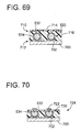
- Figs. 69 and 70 show another embodiment in which N-type and P-type electrode portions are formed on opposite sides of a photovoltaic-element holding member, respectively.
- photovoltaic elements 520 are fixed to a support plate 700 via an N-type-layer electrode portion 702 (this is an N-type-layer-electrode-portion forming step). More specifically described, in a state in which the photovoltaic elements 520 are held in contact with the N-type-layer electrode portion 702, the elements 520 and the electrode portion 702 are heated so that the elements 520 are electrically connected to the electrode portion 702.
- a light-transmitting layer 710 is moved toward the support plate 700 to which the photovoltaic elements 520 are fixed, so that the electrodes 520 are embedded in the layer 710 and thus a photovoltaic-element holding member 712 is produced.
- the light-transmitting layer 710 includes a plate member 714, and a resin layer 716 in a gel state. It is preferred that the resin layer 716 have a higher viscosity than that of the light-transmitting layer 512 employed in the above-described embodiments.
- the N-type-layer-electrode-portion forming step precedes the photovoltaic-element-holding-member producing step.
- a portion of the light-transmitting layer 710 is removed with respective portions of the photovoltaic elements 520, and an electrically insulating layer 720 is formed (this is an insulating-layer forming step).
- respective portions of the insulating layer 720 that correspond to the respective P-type layers 532 of the photovoltaic elements 520 are removed, and a P-type-layer electrode portion 722 is formed (this is a P-type-layer-electrode-portion forming step).
- the two electrode portions 702, 722 are formed on the opposite sides of the photovoltaic-element holding member 712, respectively, to provide a photovoltaic panel 724.
- each photovoltaic element 10, 520 may be provided by a silicon ball including a shell portion as a P-type layer and a core portion as an N-type layer, or a silicon ball additionally including an I-type layer between P-type and N-type layers.
- each photovoltaic element 10, 520 is not limited to a generally spherical member, but may be provided by a granular or tubular member that includes an outer layer as one of P-type and N-type layers and an inner layer as the other of P-type and N-type layers.
- Each photovoltaic element 10, 520 is not limited to any specific shape, so long as it includes P-type and N-type layers.
- the amount of embedding of each photovoltaic element 10, 520 in the holding layer 204, 202 or the light-transmitting layer 512, 600, 710 may be less than a half of the each element 10, 520.
- a method of producing a photovoltaic panel comprising the steps of producing a light-transmitting, photovoltaic-element holding member (22; 106; 152; 206; 340; 458) which holds, along a reference surface, a plurality of photovoltaic elements (10) each of which includes a P-type layer (12) and an N-type layer (14), and forming, on one of opposite sides of the photovoltaic-element holding member, a first electrode (32) which is electrically connected to the respective P-type layers of the photovoltaic elements, and a second electrode (60) which is electrically connected to the respective N-type layers of the photovoltaic elements.
Landscapes
- Photovoltaic Devices (AREA)
Abstract
Description
- forming a light-transmitting layer of a light-transmitting material,
- embedding at least respective portions of the photovoltaic elements in the light-transmitting layer, and
- curing the light-transmitting layer in a state in which the at least respective portions of the photovoltaic elements are embedded in the light-transmitting layer.
A method of producing a photovoltaic panel (70; 110; 160; 210), comprising the steps of producing a light-transmitting, photovoltaic-element holding member (22; 106; 152; 206; 340; 458) which holds, along a reference surface, a plurality of photovoltaic elements (10) each of which includes a P-type layer (12) and an N-type layer (14), and forming, on one of opposite sides of the photovoltaic-element holding member, a first electrode (32) which is electrically connected to the respective P-type layers of the photovoltaic elements, and a second electrode (60) which is electrically connected to the respective N-type layers of the photovoltaic elements.
Claims (28)
- A method of forming a photovoltaic panel (70; 110; 160; 210), comprising the steps of:providing a light-transmitting, photovoltaic-element holding member (22; 106; 152; 206; 340; 458) holding a plurality of photovoltaic elements (10) each of which includes a P-type layer (12) and an N-type layer (14), andforming, on one side of the photovoltaic-element holding member, both a first electrode (32) which is electrically connected to the respective P-type layers of the photovoltaic elements, and a second electrode (60) which is electrically connected to the respective N-type layers of the photovoltaic elements.
- A method according to Claim 1, comprising the steps of:providing a light-transmitting member (16; 100) having a plurality of photovoltaic-element holding portions (18; 104), andholding, with the photovoltaic-element holding portions, the photovoltaic elements (10), respectively.
- A method according to Claim 1 or Claim 2, comprising the steps of:forming a light-transmitting layer (202; 312) of a light-transmitting material,embedding at least respective portions of the photovoltaic elements (10) in the light-transmitting layer, andcuring the light-transmitting layer when said portions of the photovoltaic elements are embedded in the light-transmitting layer.
- A method according to Claim 3, wherein the step of embedding comprises:temporarily holding, with a surface (452) of a holding member (454), the photovoltaic elements (10), andmoving the holding member holding the photovoltaic element toward the light-transmitting layer (312), until the respective portions of the photovoltaic elements are embedded in the light-transmitting layer.
- A method according to Claim 4, wherein the step of moving comprises pressing, in a state in which the photovoltaic elements (10) contact the light-transmitting layer (312), the holding member (450) and the light-transmitting layer (312) against each other.
- A method according to any one of Claims 3 to 5, wherein the step of forming the light-transmitting layer comprises supplying the light-transmitting material to a container (310) to thereby form the light-transmitting layer (312).
- According to Claim 1, comprising the steps of:arranging, in a predetermined manner, a plurality of transparent spherical members (150) along a reference plane, andholding, with the arranged spherical members, the photovoltaic elements (10), such that the photovoltaic elements are positioned on the spherical members.
- A method according to any one of Claims 4 to 7, wherein the holding member (450) is formed of an elastic material, and wherein the step of temporarily holding comprises stretching the holding member holding the photovoltaic elements (10), to change a space between each pair of adjacent photovoltaic elements of said plurality of photovoltaic elements.
- A photovoltaic panel comprising:a light-transmitting member holding a plurality of photovoltaic elements each of which includes a P-type layer and an N-type layer; andon one side of said member, both a first electrode electrically connected to the P-type layers of the photovoltaic elements and a second electrode electrically connected to the N-type layers of the photovoltaic elements.
- A photovoltaic panel (70; 110; 160; 210), comprising:a plurality of photovoltaic elements (10) each of which includes a P-type layer (12) and an N-type layer (14);a first electrode (32) which is provided to one of two opposite sides of a first plane intersecting the photovoltaic elements and which is electrically connected to the respective P-type layers of the photovoltaic elements;a second electrode (60) which is provided to said one of the opposite sides of the first plane and which is electrically connected to the respective N-type layers of the photovoltaic elements; anda light-transmitting layer (16; 100; 150, 156; 200; 202; 312) which is formed of a light-transmitting material and which is provided to the other side of the first plane and which fills at least a space between the first plane and a second plane which is parallel to the first plane and is tangent to the photovoltaic elements.
- A photovoltaic panel according to Claim 10, wherein the first plane divides each of the photovoltaic elements (10) into a first portion whose volume is smaller than 50% of a volume of said each photovoltaic element, and a second portion whose volume is greater than 50% of the volume, and wherein the light-transmitting layer (16; 100; 150, 156; 200; 202; 312) is provided to the other side of the first plane on which the respective second portions of the photovoltaic elements are located.
- A photovoltaic panel according to Claim 10 or Claim 11, wherein the light-transmitting layer (16; 100; 150, 156; 200; 202; 312) has a shape having two plane surfaces parallel to each other, and wherein one of the two plane surfaces is substantially parallel to the first plane and the other plane surface is substantially parallel to the second plane.
- A method of producing a photovoltaic panel (564; 724), comprising the steps of:wherein the step of producing comprises:producing a light-transmitting, photovoltaic-element holding member (540; 680; 712) which holds a plurality of photovoltaic elements (520), andforming at least one electrode (550, 560; 702, 722) which is electrically connected to the photovoltaic elements held by the photovoltaic-element holding member,forming a light-transmitting layer (512; 604; 716) of a light-transmitting material,embedding at least respective portions of the photovoltaic elements in the light-transmitting layer, andcuring the light-transmitting layer when said at least respective portions of the photovoltaic elements are embedded in the light-transmitting layer.
- A method according to Claim 13, wherein the step of embedding comprises embedding more than 50% of a volume of each of the photovoltaic elements (520) in the light-transmitting layer (512; 604; 716).
- A method according to Claim 13 or Claim 14, wherein the step of embedding comprises embedding more than 50% of an area of junction of a P-type layer and an N-type layer of each of the photovoltaic elements (520) in the light-transmitting layer (512; 604; 716).
- A method according to any one of Claims 13 to 15, wherein the step of embedding comprises embedding, in the light-transmitting layer (512; 604; 716), the photovoltaic elements (520) such that an electric-power generating efficiency per unit area of the photovoltaic panel (564, 724) is higher than a predetermined value.
- A method according to any one of Claims 13 to 16, wherein the step of curing comprises at least one of heating the light-transmitting layer (512; 604; 716), cooling the light-transmitting layer, and exposing the light-transmitting layer to light.
- A method according to any one of Claims 13 to 17, wherein the step of embedding comprises:temporarily holding, with a holding surface (522; 652) of a holding member (518; 650), the photovoltaic elements (520),moving the holding member holding the photovoltaic elements toward the light-transmitting layer (512; 604) until the respective portions of the photovoltaic elements are embedded in the light-transmitting layer.
- A method according to Claim 18, wherein the step of temporarily holding comprises temporarily fixing the photovoltaic elements (520) to an adhesive layer (524; 654) which is formed on the holding surface of the holding member.
- A method according to Claim 18 or Claim 19, wherein the step of temporarily holding comprises temporarily holding, with an arranging member (526; 660), the photovoltaic elements (520) on the holding surface (522; 652) of the holding member (518; 650).
- A method according to Claim 18 or Claim 19, wherein the holding member (650) is formed of an elastic material, and wherein the step of temporarily holding comprises stretching the holding member holding the photovoltaic elements (520) to change a space between each pair of adjacent photovoltaic elements of said plurality of photovoltaic elements.
- A method according to Claim 21, wherein the step of moving the holding member comprises moving the holding member (650) toward the light-transmitting layer (512) while preventing contraction of the stretched holding member.
- A method according to any one of Claims 18 to 22, wherein the step of temporarily holding comprises:arranging, in a container (660), the photovoltaic elements (520) into a single layer such that the photovoltaic elements contact each other, andpressing the holding member (650) against the photovoltaic elements arranged in the single layer in the container.
- A method according to any one of Claims 18 to 23, wherein the step of moving comprises pressing, in a state in which the photovoltaic elements (520) contact the light-transmitting layer (512), the holding member (518; 650) and the light-transmitting layer (512) against each other.
- A method according to any one of Claims 18 to 24, wherein the step of producing further comprises removing, after the step of curing, the holding member (518; 650) from the cured light-transmitting layer (512).
- A method according to any one of Claims 13 to 25, wherein the step of forming the light-transmitting layer comprises supplying the light-transmitting material to a container (310) to thereby form the light-transmitting layer (312).
- A method according to any one of Claims 13 to 26, wherein the step of forming said at least one electrode comprises forming two electrodes (550, 560) both on one of opposite sides of the photovoltaic-element holding member (540).
- A method according to any one of Claims 13 to 26, wherein the step of forming said at least one electrode comprises forming two electrodes (702, 722) on respective sides of the photovoltaic-element holding member (712).
Applications Claiming Priority (4)
| Application Number | Priority Date | Filing Date | Title |
|---|---|---|---|
| JP2001006543 | 2001-01-15 | ||
| JP2001006544 | 2001-01-15 | ||
| JP2001006544 | 2001-01-15 | ||
| JP2001006543 | 2001-01-15 |
Publications (2)
| Publication Number | Publication Date |
|---|---|
| EP1223624A2 true EP1223624A2 (en) | 2002-07-17 |
| EP1223624A3 EP1223624A3 (en) | 2003-10-29 |
Family
ID=26607705
Family Applications (1)
| Application Number | Title | Priority Date | Filing Date |
|---|---|---|---|
| EP02250193A Withdrawn EP1223624A3 (en) | 2001-01-15 | 2002-01-11 | Photovoltaic panel and method producing same |
Country Status (2)
| Country | Link |
|---|---|
| US (1) | US6762359B2 (en) |
| EP (1) | EP1223624A3 (en) |
Cited By (4)
| Publication number | Priority date | Publication date | Assignee | Title |
|---|---|---|---|---|
| RU2390881C1 (en) * | 2008-11-18 | 2010-05-27 | Олег Александрович Манчулянцев | Photocell |
| NL2005944C2 (en) * | 2010-12-31 | 2012-07-03 | M H Mensink Beheer B V | Solar panel, solar cell converter and method of manufacturing a solar panel. |
| US10872988B1 (en) | 2013-02-03 | 2020-12-22 | Mark R. Schroeder | Photovoltaic device |
| US11538949B2 (en) | 2013-02-03 | 2022-12-27 | Mark R. Schroeder | Sensor comprising a photovoltaic device |
Families Citing this family (40)
| Publication number | Priority date | Publication date | Assignee | Title |
|---|---|---|---|---|
| WO2003010143A1 (en) * | 2001-07-26 | 2003-02-06 | Samsung Electronics Co., Ltd. | Dialkylhydroxybenzoic acid derivatives containing metal chelating groups and their therapeutic uses |
| US7535019B1 (en) | 2003-02-18 | 2009-05-19 | Nanosolar, Inc. | Optoelectronic fiber |
| CN1771641A (en) * | 2003-06-09 | 2006-05-10 | 京半导体股份有限公司 | Generator system |
| AU2004317236B2 (en) | 2004-03-12 | 2008-05-22 | Sphelar Power Corporation | Multilayer solar cell |
| US7394016B2 (en) * | 2005-10-11 | 2008-07-01 | Solyndra, Inc. | Bifacial elongated solar cell devices with internal reflectors |
| US7196262B2 (en) * | 2005-06-20 | 2007-03-27 | Solyndra, Inc. | Bifacial elongated solar cell devices |
| US8344238B2 (en) * | 2005-07-19 | 2013-01-01 | Solyndra Llc | Self-cleaning protective coatings for use with photovoltaic cells |
| US7259322B2 (en) * | 2006-01-09 | 2007-08-21 | Solyndra, Inc. | Interconnects for solar cell devices |
| US20070215195A1 (en) * | 2006-03-18 | 2007-09-20 | Benyamin Buller | Elongated photovoltaic cells in tubular casings |
| US8183458B2 (en) | 2007-03-13 | 2012-05-22 | Solyndra Llc | Photovoltaic apparatus having a filler layer and method for making the same |
| US20090014055A1 (en) * | 2006-03-18 | 2009-01-15 | Solyndra, Inc. | Photovoltaic Modules Having a Filling Material |
| US20070215197A1 (en) * | 2006-03-18 | 2007-09-20 | Benyamin Buller | Elongated photovoltaic cells in casings |
| US20080302418A1 (en) * | 2006-03-18 | 2008-12-11 | Benyamin Buller | Elongated Photovoltaic Devices in Casings |
| US20080029152A1 (en) * | 2006-08-04 | 2008-02-07 | Erel Milshtein | Laser scribing apparatus, systems, and methods |
| US7879685B2 (en) * | 2006-08-04 | 2011-02-01 | Solyndra, Inc. | System and method for creating electric isolation between layers comprising solar cells |
| JP5032496B2 (en) * | 2006-11-17 | 2012-09-26 | 京セミ株式会社 | Stacked solar cell device |
| US20080178927A1 (en) * | 2007-01-30 | 2008-07-31 | Thomas Brezoczky | Photovoltaic apparatus having an elongated photovoltaic device using an involute-based concentrator |
| US20080196759A1 (en) * | 2007-02-16 | 2008-08-21 | Thomas Brezoczky | Photovoltaic assembly with elongated photovoltaic devices and integrated involute-based reflectors |
| US8106292B2 (en) | 2007-04-30 | 2012-01-31 | Solyndra Llc | Volume compensation within a photovoltaic device |
| US8093493B2 (en) * | 2007-04-30 | 2012-01-10 | Solyndra Llc | Volume compensation within a photovoltaic device |
| US20100147367A1 (en) * | 2007-04-30 | 2010-06-17 | Cumpston Brian H | Volume Compensation Within a Photovoltaic Device |
| US20090078303A1 (en) * | 2007-09-24 | 2009-03-26 | Solyndra, Inc. | Encapsulated Photovoltaic Device Used With A Reflector And A Method of Use for the Same |
| US8017859B2 (en) * | 2007-10-17 | 2011-09-13 | Spansion Llc | Photovoltaic thin coating for collector generator |
| US20120325199A1 (en) * | 2008-05-19 | 2012-12-27 | Tyler Sims | Lens systems for solar energy solutions |
| US20120305076A1 (en) * | 2008-05-19 | 2012-12-06 | Tyler Sims | Lens systems for solar energy solutions |
| DE102008040147A1 (en) * | 2008-07-03 | 2010-01-28 | Crystalsol Og | Process for producing a monocrystalline membrane for a solar cell and monocrystal membrane together with a solar cell |
| US20130087200A1 (en) * | 2010-06-17 | 2013-04-11 | University Of Florida Research Foundation, Inc. | Enhanced thin film solar cell performance using textured rear reflectors |
| ES2599370T3 (en) * | 2011-06-23 | 2017-02-01 | Big Solar Limited | Method for manufacturing a structure comprising coating steps and corresponding device |
| GB201301683D0 (en) | 2013-01-30 | 2013-03-13 | Big Solar Ltd | Method of creating non-conductive delineations with a selective coating technology on a structured surface |
| US9957037B2 (en) * | 2013-07-10 | 2018-05-01 | X Development Llc | High altitude aircraft with integrated solar cells, and associated systems and methods |
| GB2549132A (en) | 2016-04-07 | 2017-10-11 | Big Solar Ltd | Aperture in a semiconductor |
| GB2549133B (en) | 2016-04-07 | 2020-02-19 | Power Roll Ltd | Gap between semiconductors |
| GB2549134B (en) | 2016-04-07 | 2020-02-12 | Power Roll Ltd | Asymmetric groove |
| GB201617276D0 (en) | 2016-10-11 | 2016-11-23 | Big Solar Limited | Energy storage |
| US10469027B2 (en) | 2017-01-03 | 2019-11-05 | Saudi Arabian Oil Company | Maintaining a solar power module |
| US10374546B2 (en) | 2017-01-03 | 2019-08-06 | Saudi Arabian Oil Company | Maintaining a solar power module |
| US10396708B2 (en) | 2017-01-03 | 2019-08-27 | Saudi Arabian Oil Company | Maintaining a solar power module |
| GB2588750A (en) | 2019-10-16 | 2021-05-12 | Norfib As | Wafer |
| AU2022344183A1 (en) * | 2021-09-10 | 2024-03-14 | Leap Photovoltaics Inc. | Methods and systems for photovoltaic devices using silicon particles |
| CN222602345U (en) * | 2024-03-05 | 2025-03-11 | 赫里欧新能源有限公司 | Novel photovoltaic module |
Family Cites Families (15)
| Publication number | Priority date | Publication date | Assignee | Title |
|---|---|---|---|---|
| US2904613A (en) * | 1957-08-26 | 1959-09-15 | Hoffman Electronics Corp | Large area solar energy converter and method for making the same |
| US3040416A (en) * | 1959-05-13 | 1962-06-26 | Hoffman Electronics Corp | Method of making a large area solar cell panel |
| US3025335A (en) * | 1960-02-29 | 1962-03-13 | Hoffman Electronics Corp | Flexible solar energy converter panel |
| NL298750A (en) * | 1962-10-03 | |||
| NL7202215A (en) * | 1972-02-19 | 1973-08-21 | ||
| US3998659A (en) | 1974-01-28 | 1976-12-21 | Texas Instruments Incorporated | Solar cell with semiconductor particles and method of fabrication |
| US4021323A (en) * | 1975-07-28 | 1977-05-03 | Texas Instruments Incorporated | Solar energy conversion |
| JPH0754855B2 (en) | 1984-09-04 | 1995-06-07 | テキサス インスツルメンツ インコーポレイテッド | How to make a solar array |
| US4721649A (en) | 1985-05-08 | 1988-01-26 | Minnesota Mining And Manufacturing Company | Retroreflective sheeting |
| JPS6484467A (en) | 1987-09-28 | 1989-03-29 | Kyocera Corp | Sheet-shaped sliding member |
| JPH0376273A (en) | 1989-08-18 | 1991-04-02 | Mitsubishi Electric Corp | Semiconductor substrate of solar cell |
| US5468304A (en) | 1994-03-14 | 1995-11-21 | Texas Instruments Incorporated | Output-increasing, protective cover for a solar cell |
| JPH07335925A (en) | 1994-06-03 | 1995-12-22 | Hitachi Ltd | Solar cell |
| JP2001210843A (en) * | 1999-11-17 | 2001-08-03 | Fuji Mach Mfg Co Ltd | Photovoltaic panel and manufacturing method thereof |
| US6620997B2 (en) * | 2000-10-30 | 2003-09-16 | Kyocera Corporation | Photoelectric conversion device |
-
2001
- 2001-12-31 US US10/029,998 patent/US6762359B2/en not_active Expired - Fee Related
-
2002
- 2002-01-11 EP EP02250193A patent/EP1223624A3/en not_active Withdrawn
Cited By (4)
| Publication number | Priority date | Publication date | Assignee | Title |
|---|---|---|---|---|
| RU2390881C1 (en) * | 2008-11-18 | 2010-05-27 | Олег Александрович Манчулянцев | Photocell |
| NL2005944C2 (en) * | 2010-12-31 | 2012-07-03 | M H Mensink Beheer B V | Solar panel, solar cell converter and method of manufacturing a solar panel. |
| US10872988B1 (en) | 2013-02-03 | 2020-12-22 | Mark R. Schroeder | Photovoltaic device |
| US11538949B2 (en) | 2013-02-03 | 2022-12-27 | Mark R. Schroeder | Sensor comprising a photovoltaic device |
Also Published As
| Publication number | Publication date |
|---|---|
| EP1223624A3 (en) | 2003-10-29 |
| US6762359B2 (en) | 2004-07-13 |
| US20020109957A1 (en) | 2002-08-15 |
Similar Documents
| Publication | Publication Date | Title |
|---|---|---|
| US6762359B2 (en) | Photovoltaic panel and method of producing same | |
| EP2789021B1 (en) | High concentration photovoltaic modules and methods of fabricating the same | |
| CN103782395B (en) | Concentration type photovoltaic battery module, concentration type photovoltaic battery plate and the flexible print circuit for concentration type photovoltaic battery module | |
| EP2682797B1 (en) | Method for manufacturing lens module, and lens module | |
| US7457490B2 (en) | Micro-optics on optoelectronics | |
| CN103474493B (en) | Encapsulated layer is applied to the photovoltaic module backboard comprising back-contact battery | |
| CN102224598B (en) | Solar cell module and manufacturing method thereof | |
| US20090314330A1 (en) | Photovoltaic module | |
| EP1511086A1 (en) | LIGHT−RECEIVING PANEL OR LIGHT−EMITTING PANEL, AND MANUFACTURING METHOD THEREOF | |
| JP5706794B2 (en) | Interposer with microspring contacts, and method of making and using the interposer | |
| KR20100036315A (en) | Solar cell module manufacturing method | |
| WO2008041502A1 (en) | Solar cell, light concentrating photovoltaic power generation module, light concentrating photovoltaic power generation unit, solar cell manufacturing method and solar cell manufacturing apparatus | |
| US10680127B2 (en) | Power generation circuit unit | |
| KR20100014920A (en) | A substrate assembly, an assembly process, and an assembly apparatus | |
| EP1882130A1 (en) | Concentrating solar collector | |
| US10663698B2 (en) | Optical assemblies including a spacer adhering directly to a substrate | |
| CN1856882B (en) | Integrated semiconductor solar cell tandem device and its manufacturing method and photoelectric model | |
| Deng et al. | Curved display based on programming origami tessellations | |
| US20190148143A1 (en) | A method of forming an apparatus comprising quantum dots | |
| US20080122055A1 (en) | Method and system for fabricating semiconductor components with lens structures and lens support structures | |
| KR101919482B1 (en) | A solar cell and a method for manufacturing a solar cell | |
| US20100013041A1 (en) | Microelectronic imager packages with covers having non-planar surface features | |
| CN119364925A (en) | Optical shielding element for photovoltaic cell and photovoltaic cell | |
| US20160380141A1 (en) | Solar cell module | |
| CN118098069A (en) | Screen assembly, preparation method and electronic device |
Legal Events
| Date | Code | Title | Description |
|---|---|---|---|
| PUAI | Public reference made under article 153(3) epc to a published international application that has entered the european phase |
Free format text: ORIGINAL CODE: 0009012 |
|
| AK | Designated contracting states |
Kind code of ref document: A2 Designated state(s): AT BE CH CY DE DK ES FI FR GB GR IE IT LI LU MC NL PT SE TR |
|
| AX | Request for extension of the european patent |
Free format text: AL;LT;LV;MK;RO;SI |
|
| PUAL | Search report despatched |
Free format text: ORIGINAL CODE: 0009013 |
|
| AK | Designated contracting states |
Kind code of ref document: A3 Designated state(s): AT BE CH CY DE DK ES FI FR GB GR IE IT LI LU MC NL PT SE TR |
|
| AX | Request for extension of the european patent |
Extension state: AL LT LV MK RO SI |
|
| 17P | Request for examination filed |
Effective date: 20031121 |
|
| 17Q | First examination report despatched |
Effective date: 20040311 |
|
| AKX | Designation fees paid |
Designated state(s): DE FR GB IT |
|
| GRAP | Despatch of communication of intention to grant a patent |
Free format text: ORIGINAL CODE: EPIDOSNIGR1 |
|
| RTI1 | Title (correction) |
Free format text: PHOTOVOLTAIC PANEL AND METHOD OF PRODUCING SAME |
|
| STAA | Information on the status of an ep patent application or granted ep patent |
Free format text: STATUS: THE APPLICATION IS DEEMED TO BE WITHDRAWN |
|
| 18D | Application deemed to be withdrawn |
Effective date: 20080411 |