EP1223622A2 - Semiconductor device and method for fabrication thereof - Google Patents
Semiconductor device and method for fabrication thereof Download PDFInfo
- Publication number
- EP1223622A2 EP1223622A2 EP01308381A EP01308381A EP1223622A2 EP 1223622 A2 EP1223622 A2 EP 1223622A2 EP 01308381 A EP01308381 A EP 01308381A EP 01308381 A EP01308381 A EP 01308381A EP 1223622 A2 EP1223622 A2 EP 1223622A2
- Authority
- EP
- European Patent Office
- Prior art keywords
- film
- electrode
- semiconductor device
- ferroelectric
- ferroelectric film
- Prior art date
- Legal status (The legal status is an assumption and is not a legal conclusion. Google has not performed a legal analysis and makes no representation as to the accuracy of the status listed.)
- Withdrawn
Links
Images






Classifications
-
- H—ELECTRICITY
- H10—SEMICONDUCTOR DEVICES; ELECTRIC SOLID-STATE DEVICES NOT OTHERWISE PROVIDED FOR
- H10D—INORGANIC ELECTRIC SEMICONDUCTOR DEVICES
- H10D84/00—Integrated devices formed in or on semiconductor substrates that comprise only semiconducting layers, e.g. on Si wafers or on GaAs-on-Si wafers
- H10D84/80—Integrated devices formed in or on semiconductor substrates that comprise only semiconducting layers, e.g. on Si wafers or on GaAs-on-Si wafers characterised by the integration of at least one component covered by groups H10D12/00 or H10D30/00, e.g. integration of IGFETs
-
- H—ELECTRICITY
- H10—SEMICONDUCTOR DEVICES; ELECTRIC SOLID-STATE DEVICES NOT OTHERWISE PROVIDED FOR
- H10D—INORGANIC ELECTRIC SEMICONDUCTOR DEVICES
- H10D1/00—Resistors, capacitors or inductors
- H10D1/60—Capacitors
- H10D1/68—Capacitors having no potential barriers
- H10D1/682—Capacitors having no potential barriers having dielectrics comprising perovskite structures
- H10D1/684—Capacitors having no potential barriers having dielectrics comprising perovskite structures the dielectrics comprising multiple layers, e.g. comprising buffer layers, seed layers or gradient layers
-
- H—ELECTRICITY
- H10—SEMICONDUCTOR DEVICES; ELECTRIC SOLID-STATE DEVICES NOT OTHERWISE PROVIDED FOR
- H10D—INORGANIC ELECTRIC SEMICONDUCTOR DEVICES
- H10D1/00—Resistors, capacitors or inductors
- H10D1/60—Capacitors
- H10D1/68—Capacitors having no potential barriers
- H10D1/692—Electrodes
Definitions
- the present invention relates to a semiconductor device and a method for fabricating the semiconductor device, more specifically a semiconductor device including capacitors.
- a FRAM Fluoro-electric Random Access Memory
- FRAMS have rewriting speed as high as tens of nanoseconds and has good repeatability of 1x10 10 to 1x10 12 rewritable times. Furthermore, FRAMS have small electric power consumptions. Because of these factors, FRAMS have considerable potential. FRAMS which can retain data when power supply is absent are expected to be applied to various uses, such as memories of portable instruments, etc.
- FIG. 13 is a conceptual view of a capacitor of a conventional FRAM.
- a bottom electrode 132 is formed on a silicon substrate (not shown) through a silicon oxide film, (also not shown).
- a ferroelectric film 136 is formed on the bottom electrode 132.
- a top electrode 140 is formed on the ferroelectric film 136.
- the bottom electrode 132, the ferroelectric film 136 and the top electrode 140 constitute the capacitor 142 of the FRAM.
- the ferroelectric film 136 of such capacitors 142 can be a PZT (PbZr X Ti 1-X O 3 ) film, a SBT (SrBi 2 Ta 2 O 9 ) film or others.
- the bottom electrode 132 and the top electrode 140 of the capacitors are formed of Pt, Ir or others, which have strong self-orientation and low reactivity.
- Pt, Ir, etc. are materials which tend to be self-oriented in (111). Where the bottom electrode and the top electrode are formed of such materials, crystal directions of the surfaces of the bottom electrode and the top electrodes can be easily aligned. Accordingly, in such cases, crystal directions of the ferroelectric film can be easily aligned, and the ferroelectric film can have good perovskite crystal structure. Furthermore, Pt, Ir, etc. are not easily oxidized by heat processing at high temperatures. Conventionally Pt, Ir, etc. have been used as materials of the bottom electrode 132 and the top electrode 140 of the capacitors.
- Pt, Ir, etc. are noble metals and expensive to use for forming the bottom electrode and the top electrode and their market prices are not constant. This has been a barrier to low costs of the semiconductor devices. These unreactive metals, as opposed to base metals generally do not easily undergo chemical changes, are not easily oxidized by heating in air and have low ionization tendency.
- the materials forming the bottom electrode and the top electrode of the capacitors have been restrictively limited to Pt, Ir, etc. This has been a barrier to simplification of the fabrication process and further improvement of electric characteristics.
- An object of the present invention is to provide a semiconductor device and a method for fabricating the semiconductor device at relatively low cost.
- a semiconductor device comprising a first electrode, a ferroelectric film formed above the first electrode, and a second electrode formed above the ferroelectric film, further comprising an intermediate layer of perovskite crystal structure formed at at least one of the boundary between the first electrode and the ferroelectric film and the boundary between the ferroelectric film and the second electrode.
- Base metals can be used as a material of the bottom electrode and the top electrode of the ferroelectric capacitor, which decreases costs of semiconductor devices. Materials which have previously been unsuitable to use for the top and bottom electrodes of a ferroelectric capacitor can now be used in a simple fabrication processes whereby a capacitor having improved electric characteristics is produced.
- a semiconductor device comprising a capacitor according to the first aspect of the invention and a transistor connected to the first electrode or the second electrode.
- a method for fabricating a semiconductor device comprising the step of forming a first electrode, the step of forming a ferroelectric film above the first electrode, and the step of forming a second electrode above the ferroelectric film, further comprising the step of forming an intermediate layer which is crystallizable into perovskite structure after the step of forming the first electrode and before the step of forming the ferroelectric film and/or after the step of forming the ferroelectric film and before the step of forming the second electrode.
- intermediate layers are each formed between the bottom electrode and the ferroelectric film and between the ferroelectric film and the top electrode.
- the intermediate layer is formed of a material which, even in a case that the intermediate layer is formed on the bottom electrode of a material of weak self-orientation, can be crystallized into perovskite structure.
- the intermediate layer is formed of a material which can prevent oxidation of the bottom electrode and the top electrode, and furthermore can depress transition of elements in the ferroelectric film into the bottom electrode and the top electrode.
- the intermediate layers allow the ferroelectric film to have crystal structure exhibiting ferroelectricity even in a case that materials of weak self-orientation, such as base metal, are used as materials of the bottom and top electrodes of a ferroelectric capacitor.
- materials of weak self-orientation such as base metal
- inexpensive base metals can be used as materials of the bottom and top electrodes of a ferroelectric capacitor, whereby semiconductor devices can have low costs.
- materials which have been difficult to be used as materials of the bottom electrode and the top electrode of a ferroelectric capacitor can be used, whereby fabrication processes can be further simplified, and electric characteristics can be improved.
- the semiconductor device according to a first embodiment of the present invention and a method for fabricating the same will be explained with reference to FIGs. 1A to 5.
- the term semiconductor device is used to denote both a capacitor 42, 42a etc which embodies, in itself, the inventive principle and also an overall device which incorporates such a capacitor.
- an element isolation film 14 for defining element regions 12 is formed on a silicon substrate 10.
- transistors are formed including gate electrodes 18 having a sidewall insulation film 16 formed on the side walls and a source/drain diffused layer 20.
- an inter-layer insulation film 22 of 600 nm-thickness silicon oxide film is formed on the entire surface.
- Contact holes 23 are formed in the inter-layer insulation film 22 down to the source/drain diffused layer 20.
- Conductor plugs 24a, 24b are formed in the contact holes 23.
- a 100 nm-thick silicon oxide nitride stopper film 26 is formed on the inter-layer insulation film 22.
- a 250 nm-thick silicon oxide film 28 is formed on the stopper film 26.
- a 200 nm-thick TiN adhesion layer film 30 is formed on the silicon oxide film 28.
- a 100 nm-thick Ni bottom film electrode 32 is formed on the adhesion layer 30.
- a 20 nm-thick BTO (BaTiO 3 ) intermediate film layer 34 is formed on the bottom electrode 32.
- BTO is a dielectric having perovskite crystal structure.
- PZT is a Pb-containing oxide ferroelectric having perovskite crystal structure, i.e., a lead-based oxide ferroelectric.
- a 20 nm-thick BTO intermediate film layer 38 is formed on the ferroelectric film 36.
- An 80 nm-thick Ni top electrode film is formed on the intermediate layer 38.
- the bottom electrode 32, the intermediate layer 34, the ferroelectric film 36, the intermediate layer 38 and the top electrode 40 constitute a capacitor 42 for a memory device.
- a 300 nm-thick silicon oxide film 44 is formed on the entire surface.
- Contact holes 46 extend to the top electrode 40, and a contact hole 48 which extends to the conductor plug 24a are formed in the silicon oxide film 44.
- An interconnection layer 50 interconnecting the top electrode 40 and the conductor plug 24a via the contact holes 46, 48 is formed on the silicon oxide film 44.
- a 300 nm-thickness silicon oxide inter-layer insulation film 52 is formed on the entire surface.
- a contact hole 54 which extends to the conductor plug 24b is formed in the inter-layer insulation film 52, the silicon oxide films 44, 28 and the stopper film 26.
- a bit line 56 formed on the inter-layer insulation film 52 is connected to the conductor plug 24b via the contact hole 54.
- a semiconductor device is characterized mainly in that the bottom electrode 32 and the top electrode 40 are formed of Ni, a base metal, and the intermediate layers 34, 38 each of BTO are formed respectively between the bottom electrode 32 and the ferroelectric film 36 and between the ferroelectric film 36 and the top electrode 40.
- the term base metal has opposite significance to the term noble metal, and generally means metals which are not chemically stable, tend to be oxidized by heating in air and have high ionization tendency.
- Pt, Ir, etc. are materials which tend to be self-oriented, and when the bottom electrode and the top electrode are formed of such material, the crystal directions of the surfaces of the bottom electrode and the top electrode can be easily aligned. Accordingly, when the bottom electrode and the top electrode are formed of Pt, Ir or others, crystal directions of the ferroelectric film can be easily aligned, which makes it possible for the ferroelectric film to exhibit good ferroelectricity and have perovskite crystal structure.
- Pt, Ir, etc. are not easily oxidized by thermal processing even at high temperatures. Accordingly, Pt. Ir, etc. have been used as materials of bottom electrodes 132 and top electrodes 140 in the capacitors as shown in FIG. 13.
- base metals such as Ni
- base metals such as Ni
- the ferroelectric film cannot have crystal directions easily aligned, and consequently it is difficult to have good perovskite crystal structure.
- Pb and oxygen in a PZT film tend to be diffused into base metals.
- base metals such as Ni, etc.
- the thermal processing for crystallizing the PZT film diffuses Pb and oxygen into the bottom and top electrodes to cause defects of Pb and oxygen in the PZT film.
- defects of Pb and oxygen are caused in PZT film, the PZT film is not easily crystallized into a perovskite structure. Accordingly, a good ferroelectric film cannot be obtained. In view of this it has been difficult to use base metals, such as Ni, etc., as materials of the bottom and top electrodes of a ferroelectric capacitor.
- base metals such as Ni are used as materials of the bottom and top electrodes, they become oxidized by oxygen in the PZT film. In view of this, too, it has been difficult to use base metals, such as Ni, etc., as materials of the bottom and top electrodes of the ferroelectric capacitor.
- the present embodiment solves these problems by forming the intermediate layers 34, 38 of, for example, BTO having the following characteristics between the bottom electrode 32 and the ferroelectric film 36 and between the ferroelectric film 36 and the top electrode 40.
- a BTO film has a characteristic that even in a case that BTO film is formed directly on a base metal bottom electrode of a base metal formed of, for example, Ni, the BTO film can form perovskite crystals by thermal processing in an inert atmosphere.
- a BTO film has a characteristic of being able to depress diffusion of Pb and oxygen in the PZT film into the bottom or top electrodes of base metals, such as Ni. Accordingly, the intermediate layers of BTO are formed respectively between the bottom electrode and the PZT film and between the PZT film and the top electrode to thereby prevent the PZT film from losing the ferroelectricity and also prevent the bottom electrode and top electrodes from being oxidized.
- the intermediate layers of BTO having the above-described characteristics are formed respectively between the bottom electrode and the ferroelectric film and between the ferroelectric film and the top electrode, whereby even when base metals, such as Ni, are used as materials of the bottom and/or top electrodes ferroelectric films exhibiting ferroelectricity and perovskite crystal structure can be formed.
- the bottom and top electrodes of the ferroelectric capacitor can be formed of base metals, such as Ni, whereby the semiconductor device can have low cost.
- base metals such as Ni which have been difficult to use in the past are used as materials of the bottom and top electrodes, whereby the fabrication process can be simplified, and electric characteristics can be improved.
- the element isolation film 14 is formed on the surface of a silicon substrate 10 by LOCOS (LOCal Oxidation of Silicon) to define element regions 12.
- LOCOS LOCal Oxidation of Silicon
- the 600 nm-thick inter-layer insulation film 22 of silicon oxide is formed on the entire surface by CVD (Chemical Vapor Deposition), and the surface of the inter-layer insulation film 22 is planarized by CMP (Chemical Mechanical Polishing).
- Contact holes 23 are formed by photolithography through the inter-layer insulation film 22 down to the source/drain diffused layer 20.
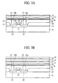
- a 20 nm-thick Ti film and a 50 nm-thick TiN film are sequentially formed on the entire surface by sputtering to form an adhesion layer (not shown) of the Ti film and the TiN film.
- a 600 nm-thick tungsten layer (not shown) is formed on the entire surface by CVD.
- the adhesion layer and the tungsten layer are formed on the inter-layer insulation film 22 and in the contact holes 23.
- the tungsten layer and the adhesion layer are polished until the surface of the inter-layer insulation film 22 is exposed by CMP to form the conductor plugs 24a, 24b of the adhesion layer and the tungsten layer buried in the contact holes 23.
- the 100 nm-thick silicon oxide nitride stopper film 26 is formed on the entire surface by CVD.
- the 250 nm-thick silicon oxide film 28 is formed on the entire surface.
- the 200 nm-thick TiN adhesion film layer 30 is formed on the entire surface by sputtering.
- a 100 nm-thick Ni film 31 for forming the bottom electrode 32 is formed in an inert atmosphere by sputtering using argon ion beams.
- the 20 nm-thick BTO (BaTiO 3 ) film for providing the intermediate layer 34 is formed on the entire surface in an inert atmosphere by sputtering using argon ion beams.
- Film forming conditions can be, e.g., 10 sccm Ar gas flow rate, 3 Pa vacuum degree, 1.5 W applied electric power, 20 second-sputtering time, and 20 to 200 °C film forming temperature.
- the BTO film 33 is formed in an inert atmosphere for the purposes of preventing oxidation of the bottom electrode of Ni and forming the BTO film of a required composition. Sputtering gives the target high transient stability, and the BTO film 33 can be formed with a required composition stabilized.
- the BTO film 33 is formed continuously without exposure to the ambient atmosphere after the Ni film 31 has been formed, so that the surface of the Ni film 31 is not contaminated, and no natural oxide film is formed on the surface of the Ni film 31.
- the step of cleaning the surface of the Ni film 31 is necessary.
- the step of cleaning the surface of the Ni film 31 is unnecessary.
- a cluster tool may be used for forming the BTO film 33 after the Ni film 31 has been formed.
- the BTO film 33 may be formed by the sol-gel process.
- the sol-gel process is a wet film-forming-method using an organic metal solution as a raw material.
- the sol-gel process allows the mixing ratio of the raw materials to be suitably changed, and the composition of the BTO film can be finely adjusted.
- the BTO film 33 is formed by sol-gel process, a cluster tool cannot be used. Accordingly it is difficult to form the BTO film 33 after the Ni film 31 has been formed, without exposure to ambient atmosphere.
- the step of cleaning the surface of the Ni film 31 before forming the BTO film 33 is necessary.
- a 200 nm-thick PZT (PbZr X Ti 1-X O 3 ) film 35 for providing the ferroelectric film 36 is formed on the entire surface without exposure to ambient atmosphere by sputtering using argon ion beams.
- Film forming conditions can be, e.g., 100 sccm Ar gas flow rate, 3 Pa vacuum degree, 2 kW applied electric power, 5 minute sputtering time, and 20 to 200 °C film forming temperature.
- the PZT film 35 is formed in an inert atmosphere for the purposes of preventing the composition of the BTO film from changing and for providing a PZT film of a required composition.
- the PZT film 35 is formed continuously without exposure to the ambient atmosphere after the BTO film 33 has been formed for the prevention of contamination, etc. of the surface of the BTO film 33.
- PZT film 35 is formed on the BTO film 33 which has not been crystallized in a perovskite structure. This causes no special problem, because the BTO film 33, the PZT film 35, etc. can be crystallized together into a perovskite structure by the thermal processing which will be described later.
- the PZT 35 may be formed by the sol-gel process.
- the PZT film 35 is formed by the sol-gel process, it is difficult to form the PZT film 35 continuously after the BTO film 33 has been formed, without exposure to the ambient atmosphere.
- a 20 nm-thick BTO film 37 for providing the intermediate layer 38 is formed on the entire surface under an inert atmosphere without exposure to ambient atmosphere for the prevention of contaimination etc of the surface of the ferroelectric film 36 by sputtering using argon ion beams.
- the BTO film 37 can be formed under, e.g., the same conditions for forming the BTO film 33.
- the BTO film 37 can be formed by sol-gel process. However, when the BTO film 37 is formed by the sol-gel process, it is difficult to form the BTO film 37 continuously after the ferroelectric film 35 has been formed, without exposure to the ambient atmosphere.
- An 80 nm-thick Ni film 39 for forming the top electrode 40 is formed on the entire surface in an inert atmosphere without exposure to ambient atmosphere by sputtering using argon ion beams.
- the Ni film 39 is formed continuously after the BTO film 37 has been formed, without exposure to the ambient atmosphere, so as to prevent the surface of the BTO film 37 from being contaminated.
- 10 minute-thermal processing of 600 °C is repeated three times in an inert atmosphere.
- An inert atmosphere can be, e.g., Ar gas.
- This thermal processing crystallizes the BTO film 33, the PZT film 35 and the BTO film 37 into perovskite structure.
- the thermal processing is made in an inert atmosphere for the purpose of preventing, for good perovskite structure crystallization, compositions of the BTO film 33, the PZT film 35, the BTO film 37, etc. from changing.
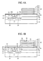
- the Ni film 39, the BTO film 37, the PZT film 35, the BTO film 33, the Ni film 31 and the adhesion layer 30 are patterned by using photolithography and dry etching.
- the capacitor 42 comprises the bottom electrode 32 of the Ni film 31, the intermediate layer 34 of the BTO film 33, the ferroelectric film 36 of the PZT film 35, the intermediate layer 38 of the BTO film 37 and the top electrode 40 of the Ni film 39.
- a 300 nm-thick silicon oxide film 44 is formed on the entire surface.
- the contact hole 46 is formed in the silicon oxide film 44 down to the top electrode 40 by photolithography, and contact hole 48 is formed in the silicon oxide films 44, 28 and the stopper film 26 down to the conductor plug 24a.
- a TiN film is formed on the entire surface. Then, the TiN film is patterned by photolithograpy to form the interconnection layer 50 interconnecting the top electrode 40 and the conductor plug 24a via the contact holes 46, 48.
- the inter-layer insulation film 52 of a 300 nm-thick silicon oxide film is formed on the entire surface.
- a contact hole 54 is formed in the inter-layer insulation film 52, the silicon oxide films 44, 28 and the stopper film 26 down to the upper surface of the conductor plug 24b by photolithography.
- a 600 nm-thick Al film is formed on the entire surface. Then, the Al film is patterned by photolithography to form the bit line 56 connected to the conductor plug 24b via the contact hole 54.
- the semiconductor device according to the present embodiment is fabricated.
- the resulting device is that of Figure 1.
- the semiconductor fabrication method according to the present modification is characterized in that the thermal processing for crystallizing the BTO film 33 into a perovskite structure occurs when the BTO film 33 has been formed, and the thermal processing for crystallizing the PZT film 35 and the BTO film 37 occurs after the PZT film 35, the BTO film 37 and the Ni film 39 have been formed.
- the fabrication steps up to the step of forming the BTO film 33 including the BTO film 33 forming step are the same as those of the semiconductor device fabrication method which has been explained above with reference to FIGs. 2A to 3A, and their explanation is not repeated.
- An inert atmosphere can be, e.g., Ar gas (see FIG. 3A).
- the PZT film 35, the BTO film 37 and the Ni film 39 are sequentially formed.
- a 5 minute-thermal processing of 600 °C is repeated three times in an inert atmosphere.
- An inert atmosphere can be, e.g., Ar gas.
- the semiconductor device of FIG. 5 according to the present embodiment is fabricated by a variant semiconductor device fabrication method.
- the semiconductor device shown in FIGs. 1A and 1B is thus fabricated by conducting, thermal processing to crystallize the BTO film 33 into the perovskite structure after the BTO film has been formed by conducting the thermal processing to crystallize the PZT film 35 and the BTO film 37 into the perovskite structure after the PZT film 35, the BTO film 37 and the Ni film 39 have been formed.
- the capacitor 42a of FIG. 6A is characterized mainly in that an intermediate layer 34a and an intermediate layer 38a are formed of BST (Ba x Sr 1-x TiO 3 ).
- a BST film has similar characteristics to a BTO (BaTiO 3 ) film. It is difficult to form a ferroelectric capacitor having good temperature characteristics by using only BST film, whose Curie temperature is not sufficiently high.
- BST film has the characteristic that even when BST film is formed directly on the bottom electrode of a base metal whose self-orientation is weak, such as Ni or others, the BST film can be crystallized into perovskite structure by thermal processing.
- the BST film like BTO film, is able to depress diffusion of Pb and oxygen within the PZT film into the bottom and top base metal electrodes formed, for example, of Ni.
- the capacitor 42b shown in FIG. 6B is characterized mainly in that STO (SrTiO 3 ) is used as a material of intermediate layers 34b, 38b.
- STO film has similar characteristics to BTO film.
- a ferroelectric capacitor can be produced using base metals as materials for the bottom and top electrodes.
- the capacitor 42c shown in FIG. 6C is characterized mainly in that CaTiO 3 film is used as a material of intermediate layers 34c, 38c. CaTiO 3 film also has similar characteristics to BTO film.
- a ferroelectric capacitor can be produced using base metals as materials for the bottom and top electrodes.
- the capacitor 42d shown in FIG. 7A is characterized mainly in that PLZT ((Pb 1-Y La Y ) (Zr 1-X Ti X )O 3 ), which is PZT with La added, is used as the material of the ferroelectric film.
- PLZT film like PZT film is a lead-based oxide ferroelectric film having perovskite crystal structure, which exhibits ferroelectricity.
- PLZT is used as a material of the ferroelectric film for the particular purpose of depressing depletion of oxygen from the ferroelectric film when thermal processing is carried out under a hydrogen atmosphere.
- the added La can suppress oxygen depletion from the PLZT film. Accordingly, even when thermal processing is carried out under a hydrogen atmosphere, a good perovskite crystal structure can be achieved, and the capacitor can exhibit good ferroelectricity.
- PLZT film is used as the ferroelectric film. Even when thermal processing is carried out under a hydrogen atmosphere, depletion of oxygen from the PLZT film can be suppressed. Accordingly, in the present modification, good perovskite crystal structure can be ensured, and a semiconductor device whose ferroelectric capacitors have good electric characteristics can be provided.
- the capacitor 42e shown in FIG. 7B is characterized mainly in that intermediate layers 34a, 38a are formed of BST, and PLZT is used as the material of a ferroelectric film 36a.
- the capacitor 42f shown in FIG. 7C is characterized mainly in that Cu is used as the material of the bottom electrode 32a and the top electrode 40a.
- Cu has low electrical resistance and high heat resistance and is a material recently much noted as an interconnection material for semiconductor devices. Accordingly, in the present modification, the top and bottom electrodes are formed integral with the interconnection layer, etc.
- materials, compositions, combinations, etc. for the intermediate layers, the ferroelectric film, the bottom electrode and the top electrode can be suitably chosen so that a ferroelectric capacitor is produced which has required characteristics.
- FIGs. 8A to 9B A semiconductor device according to a second embodiment of the present invention and a method for fabricating the same will now be explained with reference to FIGs. 8A to 9B.
- the semiconductor device according to the present embodiment is characterized mainly in that the material of the bottom electrodes is Ni, and a material of the top electrodes is Pt.
- an intermediate layer 34 of BTO is formed on the bottom Ni electrode 32.
- a PZT ferroelectric film 36 is formed on the intermediate layer 34.
- the Pt top electrode 58 is formed on the ferroelectric film 36.
- the use of Pt makes it unnecessary to form an intermediate layer between the ferroelectric film 36 and the top electrode 58.
- the bottom electrode 32, the intermediate layer 34, the ferroelectric film 36 and the top electrode 58 together constitute a capacitor 42g for a memory device.
- Ni which is an inexpensive base metal
- the semiconductor device according to the present embodiment is less expensive.
- the steps up to the step of forming the BTO film 33 including the BTO film 33 forming step are the same as those of the method for fabricating the semiconductor device according to the first embodiment described with reference to FIGs. 2A to 3A, and their explanation is not repeated.
- a 200 nm-thick PZT film 35 is formed on the ferroelectric film 36 without exposure to the ambient atmosphere.
- a 100 nm-thick Pt film 57 for forming the top electrode 58 is formed on the entire surface by sputtering without exposure to the ambient atmosphere.
- an inexpensive base metal is used as a material of only the bottom electrode, which still makes it possible to provide a semiconductor device at less cost than the conventional semiconductor device shown in FIG. 13, in which an expensive noble metal is used as material for the bottom and top electrodes.
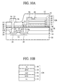
- FIGS. 10A and 10B The semiconductor device according to a third embodiment of the present invention and a method for fabricating the same will be explained with reference to FIGs. 10A to 11B.
- a ferroelectric film 60 is provided by an (AO) 2 (B Y-1 C Y O 3Y+1 ) film in which A is at least any element from Tl, Pb, Bi, and rare earth elements; B is at least one element from Bi, Pb, Ca, Sr and Ba; C is at least one element from Ti, Nb, Ta, W, Mo, Fe, Co, Cr and Zr; and Y is any of 2, 3, 4 and 5.
- A is at least any element from Tl, Pb, Bi, and rare earth elements
- B is at least one element from Bi, Pb, Ca, Sr and Ba
- C is at least one element from Ti, Nb, Ta, W, Mo, Fe, Co, Cr and Zr
- Y is any of 2, 3, 4 and 5.
- ferroelectric film of the present embodiment a crystal structure exhibiting good ferroelectricity can be formed, and a ferroelectric capacitor having good electric characteristics can be formed.
- the above-described (AO) 2 (B Y-1 C Y O 3Y+1 ) film is exemplified by one in which A is Bi, B is Sr, C is Ta, and Y is 2, i.e. SBT(SrBi 2 Ta 2 O 9 ) film.
- SBT film is a ferroelectric film having the perovskite crystal structure and Bi 2 O 3 laid one on the other, i.e., a bismuth layer structure ferroelectric film.
- Bismuth layer structure ferroelectric film exhibits good ferroelectricity as do lead-based oxide ferroelectric films.
- Bismuth layer structure ferroelectric film such as SBT film, can provide a ferroelectric film 60 exhibiting good ferroelectricity by forming intermediate layers 34, 38 as in the embodiments where PZT film is used, even when base metals, such as Ni, etc., are used as the bottom electrode 32 and the top electrode 40.
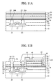
- FIG. 10A A method for fabricating a semiconductor device according to FIG. 10A will now be described with reference to FIGs. 11A and 11B.
- the step of forming BTO film 31 is the same as that in the method for fabricating the semiconductor device according to the first embodiment shown in FIGs. 2A to 3A, and its explanation is not repeated.
- a 200 nm-thick SBT film 59 which is to constitute the ferroelectric film 60 is formed on the entire surface without exposure to the ambient atmosphere by sputtering using argon ion beams.
- Film forming conditions are, e.g., 10 sccm Ar gas flow rate, 3 Pa vacuum degree, 2 kW applied electric power, 5 minutes sputtering and 20 to 200 °C film forming temperature.
- a BTO film 37 for providing the intermediate layer 38, and an Ni film 39 for providing the top electrode 40 are sequentially formed without exposure to the ambient atmosphere.
- FIG. 12A is a sectional view of the semiconductor device according to the present modification.
- the capacitor shown in FIG. 12A is characterized mainly in that a ferroelectric film 60a is provided by the above-described (AO) 2 (B Y-1 C Y O 3Y+1 ) film in which A is Bi; B is Ba; C is Ti; and Y is 3, i.e., Bi 2 Ba 2 Ti 3 O 12 .
- AO AO
- Bi 2 Ba 2 Ti 3 O 12 like SBT film is a bismuth layer structure ferroelectric film.
- a ferroelectric capacitor can be produced using a base metal as a material of the bottom electrode and the top electrode.
- the capacitor 42i shown in FIG. 12B is characterized mainly in that a ferroelectric film 60b is provided by the above-described (AO) 2 (B Y-1 C Y O 3Y+1 ) film in which A is Bi; B is Ca; C is Ti; but Y is 4, i.e., Bi 2 Ca 3 Ti 4 O 15 .
- AO AO
- Bi 2 Ca 3 Ti 4 O 15 is a bismuth layer structure ferroelectric film.
- BTO, etc. are used as the intermediate layers, but materials of the intermediate layers are not limited to the above-described materials. Any material can be used as long as the material has the above-described characteristics, i.e., the material which can be crystallized into perovskite structure even when the intermediate layers are formed on a bottom electrode of a material of weak self-orientation, can prevent the oxidation of the bottom and top electrodes that are formed of a base metal, and can suppress transition of elements in the ferroelectric film to these bottom and top electrodes.
- Materials which can satisfy the above-described conditions are, e.g., materials formed of BTO with at least one additional element from Ca, Sr, Tl, Pb, Bi, rare earth elements, Nb, Ta, W, Mo, Fe, Co, Cr and Zr added.
- Ba x (Er y Ti 1-Y )O 3 , etc. may be used as materials of the intermediate layers.
- the above-described composition ratios can be suitably adjusted so as to give the intermediate layers of required characteristics.
- the material of the ferroelectric film is not limited to the materials described hereinbefore. Any other ferroelectric film can be suitably used.
- the lead-based oxide ferroelectrics have been illustrated by means of PZT, etc.
- the lead-based oxide ferroelectric is not limited to the materials described in the embodiments, and any other lead-based oxide ferroelectrics can be suitably used.
- at least any element of La, Sr and Ca may be further added to PZT.
- PLCSZT which is a lead-based oxide ferroelectric formed of PZT with La, Ca and Sr added, can be used.
- materials of the bottom electrode and the top electrode are Ni and Cu, but any other base metals can be suitably used.
- One such metal is Cr.
- the materials of the bottom electrode and the top electrode are typically Cu and Ni.
- other elements may be added to the Cu or Ni.
- at least one element from Sc, Ti, V, Cr, Mo, Fe, Co, Y, Zr, Nb, Mn, Ta, W, Ir and Pt may be added to Ni or Cu.
- Cu and Ni can be added to Ni and Cu respectively.
- base metals such as Ni, etc.
- Relatively inexpensive noble metals may be used to achieve some cost reduction.
- Au, etc. which is less expensive than Pt, Ir, etc., can be used to thereby provide semiconductor device at lower cost than the conventional semiconductor device.
- Pt is used as the material from which the top electrode is formed.
- Such electrode is not limited to Pt.
- Pt alloys or Ir, Ir alloys, etc. may be used.
- the bottom electrode is formed of base metal, and the top electrode is formed of noble metal.
- the bottom electrode may be formed of noble metal, and the top electrode is then formed of base metal, and in this case it is necessary to form an intermediate layer between the ferroelectric film and the top electrode.
- bismuth layer structure ferroelectrics are exemplified by BST, etc.
- Bismuth layer structure ferroelectric is not limited to the materials described in the third embodiment, and any other bismuth layer structure ferroelectrics can be suitably used.
- A, B, C and Y are selected to form a bismuth layer structure ferroelectric.
- A, B, C and Y are not set so as to restrictively form a bismuth layer structure ferroelectric. They may be suitably set so as to form other ferroelectrics having required characteristics.
- the above-described embodiments have been explained by means of a FRAM. However, the present invention is not essentially applied to FRAM's and is applicable to any semiconductor devices using ferroelectrics.
- the above-described capacitor is applicable to a single capacitor. When the above-described capacitor is applied to a single capacitor, the above-described function and effects can be provided.
- the intermediate layers and the ferroelectric films are formed by sputtering and the sol-gel process.
- the intermediate layers and the ferroelectric films may be formed not only by sputtering and sol-gel process but also by other film forming processes.
- an inert gas used in forming the intermediate layers and the ferroelectric films is argon gas.
- argon gas not only argon gas but also any other inert gas can be used, and helium gas, neon gas, krypton gas, nitrogen gas, xenon gas, their mixed gases or others, for example, can be suitably used.
Landscapes
- Semiconductor Memories (AREA)
- Semiconductor Integrated Circuits (AREA)
Abstract
Description
Claims (15)
- A semiconductor device comprising a first electrode, a ferroelectric film formed above the first electrode, and a second electrode formed above the ferroelectric film, the device further comprising an intermediate layer of a perovskite crystal structure formed at at least one of the boundary between the first electrode and the ferroelectric film, and the boundary between the ferroelectric film and the second electrode.
- A semiconductor device according to claim 1, wherein the intermediate layer is a BaTiO3, SrTiO3, or CaTiO3.
- A semiconductor device according to claim 2, wherein the intermediate layer further contains at least one element from Ca, Sr, Tl, Pb, Bi, rare earth elements Nb, Ta, W, Mo, Fe, Co ,Cr, and Zr.
- A semiconductor device according to claim 1, wherein the first electrode and/or the second electrode is base metal.
- A semiconductor device according to claim 4, wherein the base metal is Ni, Cu or Cr.
- A semiconductor device according to any one of claims 1-5 wherein the ferroelectric film is lead-based oxide ferroelectric film.
- A semiconductor device according to claim 6, wherein the lead-based oxide ferroelectric film is PbZrXTi1-XO3 film.
- A semiconductor device according to claim 7, wherein the PbZrXTi1-XO3 film further contains at least any one of elements La, Sr and Ca.
- A semiconductor device according to any one of claims 1 to 5, wherein the ferroelectric film is (AO)2(BY-1CYO3Y+1) film wherein A is at least one element from Tl, Pb, Bi and rare earth element; B is at least one element from Bi, Pb, Ca, Sr and Ba; C is at least one element from Ti, Nb, Ta, W, Mo, Fe, Co, Cr and Zr; and Y is any of 2, 3, 4 and 5.
- A semiconductor device according to claim 9, wherein the ferroelectric film is bismuth layer structure ferroelectric film.
- A semiconductor device according to claim 10, wherein the bismuth layer structure ferroelectric film is SrBi2Ta2O9 film, Bi2Ba2Ti3O12 film or Bi2Ca3Ti4O15 film.
- A semiconductor device according to any preceding claim having a transistor connected to the first electrode or the second electrode.
- A method for fabricating a semiconductor device comprising the step of forming a first electrode, the step of forming a ferroelectric film above the first electrode, and the step of forming a second electrode above the ferroelectric film, further comprising the step of forming an intermediate layer which is crystallizable into perovskite structure after the step of forming the first electrode and before the step of forming the ferroelectric film and/or after the step of forming the ferroelectric film and before the step of forming the second electrode.
- A method for fabricating a semiconductor device according to claim 13, wherein in the step of forming the intermediate layer, the intermediate layer is formed in an inert atmosphere.
- A method for fabricating a semiconductor device according to claim 13 or 14, wherein the intermediate layer and the ferroelectric film are formed without there being exposure to ambient atmosphere.
Applications Claiming Priority (2)
| Application Number | Priority Date | Filing Date | Title |
|---|---|---|---|
| JP2001004150 | 2001-01-11 | ||
| JP2001004150A JP2002208678A (en) | 2001-01-11 | 2001-01-11 | Semiconductor device and manufacturing method thereof |
Publications (2)
| Publication Number | Publication Date |
|---|---|
| EP1223622A2 true EP1223622A2 (en) | 2002-07-17 |
| EP1223622A3 EP1223622A3 (en) | 2004-07-28 |
Family
ID=18872380
Family Applications (1)
| Application Number | Title | Priority Date | Filing Date |
|---|---|---|---|
| EP01308381A Withdrawn EP1223622A3 (en) | 2001-01-11 | 2001-10-01 | Semiconductor device and method for fabrication thereof |
Country Status (5)
| Country | Link |
|---|---|
| US (1) | US20020090742A1 (en) |
| EP (1) | EP1223622A3 (en) |
| JP (1) | JP2002208678A (en) |
| KR (1) | KR100421506B1 (en) |
| TW (1) | TW504836B (en) |
Families Citing this family (7)
| Publication number | Priority date | Publication date | Assignee | Title |
|---|---|---|---|---|
| US20030075778A1 (en) * | 1997-10-01 | 2003-04-24 | Patrick Klersy | Programmable resistance memory element and method for making same |
| KR100390845B1 (en) * | 2001-06-30 | 2003-07-12 | 주식회사 하이닉스반도체 | Ferroelectric capacitor in semiconductor device and forming method thereof |
| CN100420024C (en) | 2003-06-06 | 2008-09-17 | 富士通株式会社 | Manufacturing method of semiconductor device |
| JP4670612B2 (en) * | 2005-11-30 | 2011-04-13 | Tdk株式会社 | Dielectric element and manufacturing method thereof |
| JP4802777B2 (en) * | 2006-03-13 | 2011-10-26 | セイコーエプソン株式会社 | Semiconductor device and manufacturing method thereof |
| TW201738888A (en) * | 2016-04-18 | 2017-11-01 | Univ Chang Gung | Structure of memory device which comprises an intermediate layer made up of a first dielectric film and a second dielectric film between the top electrode and the bottom electrode |
| US12224309B2 (en) * | 2020-12-09 | 2025-02-11 | Intel Corporation | Capacitors with built-in electric fields |
Family Cites Families (16)
| Publication number | Priority date | Publication date | Assignee | Title |
|---|---|---|---|---|
| JP3106255B2 (en) * | 1991-08-16 | 2000-11-06 | ローム株式会社 | Ferroelectric device |
| EP0568064B1 (en) * | 1992-05-01 | 1999-07-14 | Texas Instruments Incorporated | Pb/Bi-containing high-dielectric constant oxides using a non-Pb/Bi-containing perovskite as a buffer layer |
| US5471364A (en) * | 1993-03-31 | 1995-11-28 | Texas Instruments Incorporated | Electrode interface for high-dielectric-constant materials |
| JP3435966B2 (en) * | 1996-03-13 | 2003-08-11 | 株式会社日立製作所 | Ferroelectric element and method of manufacturing the same |
| TW345723B (en) * | 1996-07-09 | 1998-11-21 | Hitachi Ltd | Semiconductor memory and process for producing the same |
| KR100247919B1 (en) * | 1996-12-31 | 2000-03-15 | 윤종용 | Capacitor having ferroelectric film |
| JP3087672B2 (en) * | 1997-01-07 | 2000-09-11 | 日本電気株式会社 | Thin film capacitors |
| JPH10247664A (en) * | 1997-03-04 | 1998-09-14 | Hitachi Ltd | Semiconductor integrated circuit device and method of manufacturing the same |
| KR19980082687A (en) * | 1997-05-08 | 1998-12-05 | 김영환 | Ferroelectric capacitor using multilayer structure and manufacturing method |
| US6777248B1 (en) * | 1997-11-10 | 2004-08-17 | Hitachi, Ltd. | Dielectric element and manufacturing method therefor |
| JP3092659B2 (en) * | 1997-12-10 | 2000-09-25 | 日本電気株式会社 | Thin film capacitor and method of manufacturing the same |
| KR20000014388A (en) * | 1998-08-20 | 2000-03-15 | 윤종용 | Ferroelectric memory capacitor and forming method thereof |
| JP3468706B2 (en) * | 1998-09-17 | 2003-11-17 | 富士通株式会社 | Semiconductor device and manufacturing method thereof |
| KR20010045568A (en) * | 1999-11-05 | 2001-06-05 | 윤종용 | Capacitor manufacturing method for preventing defect generation at subsequent annealing |
| JP2001189430A (en) * | 1999-12-28 | 2001-07-10 | Toshiba Corp | Ferroelectric capacitor |
| US6518609B1 (en) * | 2000-08-31 | 2003-02-11 | University Of Maryland | Niobium or vanadium substituted strontium titanate barrier intermediate a silicon underlayer and a functional metal oxide film |
-
2001
- 2001-01-11 JP JP2001004150A patent/JP2002208678A/en not_active Withdrawn
- 2001-09-24 US US09/960,296 patent/US20020090742A1/en not_active Abandoned
- 2001-09-27 TW TW090123953A patent/TW504836B/en not_active IP Right Cessation
- 2001-10-01 EP EP01308381A patent/EP1223622A3/en not_active Withdrawn
- 2001-10-10 KR KR10-2001-0062301A patent/KR100421506B1/en not_active Expired - Fee Related
Also Published As
| Publication number | Publication date |
|---|---|
| KR20020060563A (en) | 2002-07-18 |
| US20020090742A1 (en) | 2002-07-11 |
| KR100421506B1 (en) | 2004-03-09 |
| TW504836B (en) | 2002-10-01 |
| EP1223622A3 (en) | 2004-07-28 |
| JP2002208678A (en) | 2002-07-26 |
Similar Documents
| Publication | Publication Date | Title |
|---|---|---|
| KR100308241B1 (en) | A method for manufacturing a semiconductor device | |
| KR100244933B1 (en) | Method of manufacturing electrode | |
| US7064374B2 (en) | Barrier layers for protecting metal oxides from hydrogen degradation | |
| US6365927B1 (en) | Ferroelectric integrated circuit having hydrogen barrier layer | |
| US20060073613A1 (en) | Ferroelectric memory cells and methods for fabricating ferroelectric memory cells and ferroelectric capacitors thereof | |
| JP3665570B2 (en) | Capacitor electrode device | |
| US6204070B1 (en) | Method for manufacturing ferroelectric capacitor | |
| KR19980063403A (en) | High Temperature Electrode-Barriers for Ferroelectric Capacitors and Other Capacitor Structures | |
| KR100504318B1 (en) | Electronic material, its manufacturing method, dielectric capacitor, nonvolatile memory and semiconductor device | |
| US6392265B2 (en) | Semiconductor device | |
| US20060273366A1 (en) | Methods of manufacturing ferroelectric capacitors and semiconductor devices | |
| US20050230725A1 (en) | Ferroelectric capacitor having an oxide electrode template and a method of manufacture therefor | |
| JPH11111930A (en) | Method for manufacturing semiconductor storage element | |
| EP1223622A2 (en) | Semiconductor device and method for fabrication thereof | |
| KR100405146B1 (en) | Process for producing a structured metal oxide-containing layer | |
| US6284588B1 (en) | Method for fabricating ferroelectric memory devices capable of preventing volatility of elements in ferroelectric films | |
| US6762476B2 (en) | Dielectric element including oxide dielectric film and method of manufacturing the same | |
| US6890768B2 (en) | Method of making layered superlattice material with ultra-thin top layer | |
| US7217576B2 (en) | Method for manufacturing ferroelectric capacitor, method for manufacturing ferroelectric memory, ferroelectric capacitor and ferroelectric memory | |
| US20010051381A1 (en) | Method for manufacturing a ferroelectric memory | |
| US7456456B2 (en) | Semiconductor device and method of manufacturing the same | |
| JP2000156473A (en) | Semiconductor device, method of manufacturing the same, and method of manufacturing a capacitor | |
| US6391660B2 (en) | Method for fabricating semiconductor memory device having ferroelectric layer | |
| US6783996B2 (en) | Capacitor of semiconductor device and fabrication method thereof | |
| JP3604253B2 (en) | Semiconductor storage device |
Legal Events
| Date | Code | Title | Description |
|---|---|---|---|
| PUAI | Public reference made under article 153(3) epc to a published international application that has entered the european phase |
Free format text: ORIGINAL CODE: 0009012 |
|
| AK | Designated contracting states |
Kind code of ref document: A2 Designated state(s): AT BE CH CY DE DK ES FI FR GB GR IE IT LI LU MC NL PT SE TR |
|
| AX | Request for extension of the european patent |
Free format text: AL;LT;LV;MK;RO;SI |
|
| PUAL | Search report despatched |
Free format text: ORIGINAL CODE: 0009013 |
|
| AK | Designated contracting states |
Kind code of ref document: A3 Designated state(s): AT BE CH CY DE DK ES FI FR GB GR IE IT LI LU MC NL PT SE TR |
|
| AX | Request for extension of the european patent |
Extension state: AL LT LV MK RO SI |
|
| AKX | Designation fees paid | ||
| REG | Reference to a national code |
Ref country code: DE Ref legal event code: 8566 |
|
| STAA | Information on the status of an ep patent application or granted ep patent |
Free format text: STATUS: THE APPLICATION IS DEEMED TO BE WITHDRAWN |
|
| 18D | Application deemed to be withdrawn |
Effective date: 20050129 |