The invention relates to a method and an arrangement to determine a clock
timing error in a multicarrier transmission system.
In a multicarrier transmission system, such as a discrete multitone (DMT) transmission
system, an information symbol is transmitted simultaneously on several modulated
carriers.
Accurate timing information must be known to the receiver in order to produce
reliable estimates of the transmitted information sequence. A synchronizer determines
which samples of the received signal are to be presented to a decision device. Usually,
the timing information is not a priori known to the receiver and can be extracted from the
received signal. For transmission over an ideal channel, the received signal is a delayed
version of the transmitted signal (due to the transmission delay introduced by the
transmission channel). This delay, together with the difference in symbol clock (phase)
between transmitter and receiver is estimated by a synchronizer unit.
When signals are transmitted over a dispersive channel, equalization may be
performed by the receiver essentially with the purpose to reverse the effect of the
channel.
In order to estimate this timing error in a multicarrier transmission system, a
common method applied to DMT uses a data-aided algorithm wherein the sampling clock
is first roughly synchronized and, at least for one tone or carrier, the position, in the complex
plane, of the detected symbol is compared with the position in this plane of the
signal at the input of the decision device, and this comparison provides a phase error
which is used for correction.
This estimation may be performed either on one single pilot carrier or, in order
to reduce the noise of the estimation and the tracking range, on a combination of pilot
carriers.
The method and the arrangement according to the invention provide an
alternative which can be used for DMT transmission where the cyclic prefix is absent or
for other types of multi carrier transmission (e.g. multi-carrier systems based on filter
banks).
The arrangement according to the invention is characterized in that for timing
error correction on the receiving side of a multicarrier data, it comprises, for at least one,
and preferably, a plurality of carriers, a Mueller and Müller timing error estimator.
Such Mueller and Müller timing error estimation is already known in the art, for
instance in single carrier transmission synchronizers wherein the cascade of the
baseband equivalent of the impulse response of the transmit shaping filter and the
receiver filter impulse response is a Nyquist pulse.
According to this method, the filtered version of the timing error estimate, e,
which is used for timing correction has the following value:
This method provides an error signal which varies in function of the symbol
timing error according to a S curve which is particularly suitable for correction. The
particular shape of the S curve depends on the shape of the transmitted pulse and
on the receiver filters.
In multicarrier transmission e must be multiplied with α (α=-1 , α=1) such
that when the product αe is used in a feedback synchroniser system, a stable timing
locked loop is obtained. The value α depends on the carrier-index.
In a preferred embodiment, the timing error is estimated by the calculation
of the parameter êi for all the carriers, the multicarrier timing error signal being a
weighted average of the values of said êi parameters, the weighting coefficient of
each êi parameter depending on the carrier frequency. This weighting coefficient
depends for instance of the quality of transmission of the corresponding single
carrier channel and/or of the signal to noise ratio of the corresponding transmission
channel.
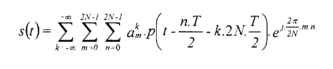
If, for example, the method is applied to the transmission of a DMT signal,
with N modulated carriers, the signal s(t) at the output of the transmitter is given by
wherein:
For a timing error (τ
e), the signal at the input of the decision device for
carrier m at t=τ
e (not taking into account the contributions of signals
transmitted over carriers other than m) is:
where
The Mueller and Müller timing error estimation applied to carrier m provides
a term proportional to
τ e e j· 2π 2N ·m .
The imaginary part of this term can be used as
estimate of the timing error τe.
In a preferred embodiment, each error signal e; is weighted according to the
quality of transmission of the corresponding channel. In fact, each carrier is considered
as transmitted on a channel which is distinct from the channel transmitting
another carrier, and the quality of transmission may differ from one channel to the
other. In that case, greater weights are given to transmissions having the best qualities
and smaller weights are given to transmissions having the lowest qualities. In an
embodiment, the weight given to each carrier channel is the signal to noise ratio
(SNR).
In brief the invention provides a reception arrangement for receiving multicarrier
symbols, each multicarrier symbol (S
1, S
2, S
3) comprising a plurality of single
carrier symbols, each single carrier symbol modulating a respective carrier
frequency (F
1, F
2, F
3), these single carrier symbols being transmitted
simultaneously, the reception arrangement comprising means for detecting the
time, or phase error, of at least one single carrier and means for correcting the
phase of a sampling clock in view of the estimated timing error,
wherein the means for estimating the timing or phase error comprise, at least
for one carrier, means (58
i ... 58
N, 24, 40) for determining a parameter ê
i for a
carrier f
i, or a quantity proportional to the parameter ê
i, according to the
following formula:
wherein r i / k is the detected signal for the single carrier at a time t, a i / k is the corresponding
single carrier symbol at the same time t, a i / k-1 and r i / k-1 correspond,
respectively, to a i / k and r i / k at time t-NT, NT being the duration of
transmission of a multicarrier symbol, and E[] means an average value on
several successive symbols.
Other features and advantages of the invention will appear with the
description of certain of its embodiments, this description being made with reference
to the herein happened drawings wherein:
The principle of multicarrier transmission will be explained with reference to
figures 1a, 1b, 1c and 2.
In figure 1a, an information sequence is having several binary information
bits is represented. For the m-th frame, the two most significant bits form a symbol
S1 which is transmitted with carrier frequency f1, the three following bits form a
symbol S2 which is transmitted with carrier frequency f2, and the two least
significant bits form a symbol S3 which is transmitted with carrier frequency f3. On
figure 1a, the symbols S1, S2 and S3 are represented with the usual diagrams in the
complex plane, these symbols being represented by circles. The black dots in the
complex plane represent the other possible values to be transmitted. In other words,
the complete constellation of values which it is possible to transmit are represented,
i.e. 4 points for 2 bits and 8 points for 3 bits.
The symbols S1, S2 and S3 modulate the corresponding carrier in
amplitude and/or in phase.
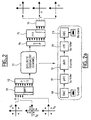
Figure 2 represents a modulator, a demodulator and a transmission
channel. More precisely, figure 2 shows that the modulator comprises an IFFT
module 11, i.e. a module providing the inverse fast Fourier transform of the carriers
f1, f2, f3 modulated by the symbols S1, S2 and S3. The parallel outputs of IFFT
module 11 are provided to inputs of a parallel/serial converter 12. The signals are
transmitted in series through a discrete equivalent channel 17 (comprising the actual
channel 13) to a receiving part comprising a demodulator including a serial/parallel
converter 14, a FFT (fast Fourier transform) module 15 receiving the parallel outputs
from the converter 14, and providing signals to a frequency equaliser module 16
which presents outputs on which appear the demodulated symbols S1, S2 and S3.
The discrete equivalent channel 17 is represented on figure 2a. It
comprises, in addition to the channel 13 itself, on the transmission side, a digital to
analog converter 18, a transmission filter 19, corresponding to the impulse response
of the transmitter filter, and on the receiving side, a filter 21 corresponding to the
impulse response of the receiver filter, and an analog to digital converter 23.
As illustrated by figure 1b, the three symbols S1, S2, S3 are converted in
continuous-time signals that are transmitted simultaneously during a time NT. The
starting points of transmission of symbols S1, S2, S3 are the same and the end
points of transmission of symbols S1, S2 and S3 appear also at the same time
instant.
The four analogs signals a0, a1, a2 and a3 (a1, a2 and a3 corresponding to
carrier frequencies f1, f2 and f3) provided by the IFFT module, which are transmitted
simultaneously, appear as a signal as on figure 1b.
Figure 1c shows the variations with time of the (useful) signals at the
outputs of the FFT module, assuming an ideal channel. More precisely, for the
signal at the i-th FFT output (i = 1,2,3), only the complex valued contribution of the i-th
carrier is shown, the contribution of the intercarrier interference to the signal being
not shown. Re (FFTi) means the real part of complex signal (FFTi) and Im (FFTi)
means the imaginary part of complex signal (FFTi).
T0 is the optimal sampling instant at the receiver. As shown, at time T0,
Re (FFT1) has a value +2 and Im (FFT1) has also a value +2. These values
correspond to symbol S1. At this time T0, Re (FFT2) has the value -2 and
Im (FFT2) has the value -1 which correspond to symbol S2 and Re (FFT3) has the
value +2 and Im (FFT3) has the value -2 which correspond to symbol S3.
T1 is the timing instant at the receiver when a timing error e= T1-T0 occurs.
The synchronizer makes use of the FFT signals at time instants T2=T1-NT and
T3=T1+NT to extract the estimated timing error.
The invention is based on the use of a Mueller and Müller synchroniser, at
least for one of the tones or carriers.
In the preferred embodiment which is represented on figure 3, use is made
of a Mueller and Müller error estimation for each carrier.
As shown on figure 3, the multicarrier, or discrete multitone, signal which is
received is sampled by an analog to digital converter 52 and applied to the input of
the series/parallel converter 14 which has a number of outputs 141, 142, ..., 14N
equal to the number of tones of the multicarrier signal. These parallel signals are
applied to a filter bank 56 which realizes a linear equalization of the received single
tones. Each single tone at the output 561, ..., 56N of the filter bank 56 is applied to
the input of a corresponding Mueller and Müller module 58i and to the input 20i of a
signal to noise ratio (SNR) estimator 20.
Each module 58i, which will be described later in more details, has an output
22i which is connected to a corresponding input 24i of a calculation module 24.
This calculation module 24 has parallel inputs 261, ..., 26N which are connected
to corresponding outputs 281, ..., 28N of a module 28 assigning weights to
the values provided on the outputs of modules 58i.
These weights provided by module 28 depend on the signal to noise ratio
on the corresponding channel.
More precisely, the block 20 which determines the signal to noise ratio of
each channel has (in the represented example) outputs 51i which are connected to
corresponding inputs 27i of module 28 and this signal to noise ratio of each channel
is provided on the corresponding output 281, ..., 28N multiplied with a weight which
depends on the carrier.
For each carrier, the calculation module 24 has a multiplier 32i which multiplies
the signal provided at the output 22i of module 58i by the weighting coefficient
provided at the corresponding output 28i of the weighting module 28.
The output of the multiplier 32i is applied to an input 34i of an adder 34.
The adder 34 has an output 36 which is connected to the numerator input 38 of a
divider 40 having a denominator input 42 connected to an output 28S of the weighting
module 28.
The signal provided on input 42 is the square root of the sum of the square
values of the weighting coefficients A1, ..., AN provided on outputs 281, ..., 28N.
The normalized signal provided on the output of divider 40 is applied to the
input of an averaging filter 46 and the output of this averaging filter is the signal
which is used for the correction of a timing unit or sampling clock 48 which is used
for the analog to digital conversion.
Each module 58i performs the following calculation:
ei = ri k-1ai* k -ri kai* k-1
In this formula, a i / k is the single tone symbol corresponding to carrier i at
time t, r i / k is the symbol measured at same time t and which differs from the symbol
a i / k because of the timing error. a i / k-1 and r i / k-1 represent, respectively, the actual
symbol and the measured symbol at time t-NT.
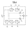
In order to obtain this value ei, each module 58i (figure 4) receives on its
input the signal r i / k and has a first branch comprising a decision circuit 60i which
determines a i / k in view of r i / k, this decision module being followed by a complex
conjugate circuit 62i which provides a i* / k.
The output a i* / k of circuit 62i is provided to the first input of a multiplier 64i
having a second input connected to the output of a delay circuit 66i of duration NT
receiving on its input the signal r i / k and providing, therefore, on its output the signal
r i / k-1 (due to the delay NT). This delay circuit 66i is followed also by another
decision circuit 68i providing on its output the symbol a i / k-1.
A circuit 70i transforms the value a i / k-1 into its complex conjugate value
and the output of this circuit 70i is connected to the first input of a multiplier 72i having
a second input receiving the signal r i / k from the output 56i of filter bank 56. The
outputs of the multipliers 64i and 72i are connected to the respective inputs of an
adder 76i which performs the calculation of formula (2) above.