EP1220261A2 - Structured lighting material, method to generate incoherent luminescence and illuminator - Google Patents
Structured lighting material, method to generate incoherent luminescence and illuminator Download PDFInfo
- Publication number
- EP1220261A2 EP1220261A2 EP01130916A EP01130916A EP1220261A2 EP 1220261 A2 EP1220261 A2 EP 1220261A2 EP 01130916 A EP01130916 A EP 01130916A EP 01130916 A EP01130916 A EP 01130916A EP 1220261 A2 EP1220261 A2 EP 1220261A2
- Authority
- EP
- European Patent Office
- Prior art keywords
- luminescent
- structured lighting
- lighting material
- unit
- luminescent unit
- Prior art date
- Legal status (The legal status is an assumption and is not a legal conclusion. Google has not performed a legal analysis and makes no representation as to the accuracy of the status listed.)
- Withdrawn
Links
Images





Classifications
-
- H—ELECTRICITY
- H01—ELECTRIC ELEMENTS
- H01J—ELECTRIC DISCHARGE TUBES OR DISCHARGE LAMPS
- H01J63/00—Cathode-ray or electron-stream lamps
- H01J63/06—Lamps with luminescent screen excited by the ray or stream
-
- H—ELECTRICITY
- H01—ELECTRIC ELEMENTS
- H01J—ELECTRIC DISCHARGE TUBES OR DISCHARGE LAMPS
- H01J63/00—Cathode-ray or electron-stream lamps
- H01J63/02—Details, e.g. electrode, gas filling, shape of vessel
- H01J63/04—Vessels provided with luminescent coatings; Selection of materials for the coatings
Definitions
- the present invention relates to a structured lighting material, method to generate incoherent luminescence and an illuminator each of which emits light when energy is applied thereto from the external.
- a luminescent device has been known as having some conventional structured lighting material.
- the present invention concerns a specific structured lighting material to be described below.
- the luminescent device has come into widespread use in display applications using a cathode-ray tube, a projection tube or the like (cf. Phosphor Handbook, by S. Shionoya and W. M. Yen, CRC Press, Boca Raton, FL, 1998). Diverse experiments on structured lighting materials including luminescent devices have been made up to now.
- a luminescent device comprises a metal-made substrate (base) 102 and a luminescent unit 103 made by placing a phosphor on the substrate 102 in the form of a layer.
- the luminescent device emits light when the host of a phosphor constituting the luminescent unit 103 is excited by electric energy such as electron beam, electric charge or electric field applied from the external.
- the luminescent device can convert the inputted electric energy (excitation energy) into luminescence to be outputted.
- the luminescence or emission intensity of the luminescent device generally increases monotonically with an increase in an excitation energy inputted from the external, the degree of increase is prone to drop if the excitation energy quantity exceeds an energy quantity; if the excitation energy quantity further increases, the luminescent intensity reaches a saturation or decreases (cf. Phosphor Handbook, by S. Shionoya and W. M. Yen, CRC Press, Boca Raton, FL, 1998, p.489-p.498).
- the input-output differential variation of the conventional luminescent device is apt to get worse as the input energy such as electron beam increases.
- the present invention has been developed in consideration of such a situation, and it is therefore an object of the invention to provide a structured lighting material wherein luminescent intensity increases superlinearly when excitation energy based on electron beam, electric charge or electric field exceeds a threshold.
- the term "superlinearly" signifies that the input-output differential variation ⁇ increases when applied energy exceeds a threshold. In most cases, when the applied energy is below the threshold, the input-output differential variation ⁇ assumes less than 1. On the other hand, it becomes 1 or more when the applied energy is above the threshold.
- a structured lighting material is characterized by comprising a luminescent unit wherein the intensity of incoherent luminescence increases superlinearly when energy applied in a non-contact manner exceeds a threshold.
- This arrangement wherein the luminescent intensity of the luminescent unit increases superlinearly when the electric energy given in a non-contact manner exceeds the threshold, can be incorporated into a wide range of applications.
- the application to various types of illuminations is feasible owing to its high-efficient luminescence.
- it is also applicable to detection equipment, alarm equipment or the like because the magnitude of the electric energy can be monitored from the luminescence intensity of the luminescent unit.
- the application to memories or various types of control devices becomes feasible because the luminescent intensity varies rapidly around a threshold so that the variation of the luminescent intensity is extracted as on/off signals in a state where reference is set to the threshold.
- the luminescent color of the luminescent unit varies as the input energy increased beyond the threshold.
- the energy is electric energy originating from any one of electron beam, electric charge and electric field.
- the luminescent part has a non-electrical conductive property.
- a structured lighting material according to the second aspect of the present invention is characterized by comprising a luminescent unit which shows a non-electrical conductive property and has a microscopic or minute uneven surface, wherein the luminescent intensity increases superlinearly when energy applied to the minute uneven surface in a non-contact manner exceeds a threshold.
- the requirement for the luminescent unit is only the realization of the minute uneven surface, and various kinds of knowledge concerned with the conventional structured lighting materials can be put directly to practical use.
- the minute uneven surface is formed in a manner that the thickness of the luminescent unit is made non-uniform.
- the minute uneven surface has high and low portions respectively corresponding to maximum and minimum thicknesses of the luminescent unit, and the maximum thickness is set to be three or more times said minimum thickness.
- the minute uneven surface has high and low portions respectively corresponding to maximum and minimum thicknesses of the luminescent unit, and the maximum thickness is set to be ten or more times said minimum thickness.
- the minimum thickness of the luminescent unit is not more than 500 ⁇ m.
- the minimum thickness of the luminescent unit is not more than 50 ⁇ m.
- an inclination angle (slope angle) of an uneven surface of a local site is in a range from 30 degrees to 150 degrees.
- an inclination angle of an uneven surface of a local site is in a range from 50 degrees to 130 degrees.
- the luminescent unit is made of inorganic material.
- the luminescent unit is adhered on a substrate.
- the luminescent unit is adhered on a substrate without using water-soluble fixing agent.
- the luminescent unit is adhered on the substrate in a manner of facilitating electrification.
- an illuminator according to the third aspect of the present invention is characterized by comprising the structured lighting material according to the first or second aspects of the present invention.
- a method to generate incoherent luminescence according to the fourth aspect of the present invention is characterized by applying energy more than a threshold to the structured lighting material including a luminescent unit wherein the intensity of incoherent luminescence increases superlinearly when energy applied in a non-contact manner exceeds the threshold.
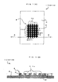
- FIGs. 1(A), 1(B), 2(A) and 2(B) are illustrations of a luminescent device according to an embodiment of the present invention.
- FIGs. 1(A) and 1(B) are illustrations of a configuration thereof, and FIG. 1(A) is an illustrative plan view while FIG. 1(B) is an illustrative enlarged cross-sectional view taken along a line X1-X1 of FIG. 1(A), and FIGs. 2(A) and 2(B) are illustrations of another configuration thereof, and FIG. 2(A) is an illustrative plan view while FIG. 2(B) is an illustrative enlarged cross-sectional view taken along a line X3-X3 of FIG. 2(A).
- this luminescent device (structured lighting material) 1 comprises a metal-made (for example, copper-made) substrate 2 and an insulation (non-electrical conductive) luminescent unit 3 adhered on the substrate 2, and grooves 4 are made in a lattice-like fashion in the luminescent unit 3.
- a luminescent material for the formation of the luminescent unit 3 requires only a non-electrical conductive property, and materials applicable to the conventional luminescent devices are also applicable as the luminescent material, for example, television red phosphor (Y 2 O 2 S:Eu, Tb), blue phosphor (SrHfO 3 :Tm) or the like put on the market.
- the insulation (non-electrical conductive) property signifies that the electrical resistivity is not below 10 6 ⁇ cm.
- a material of the electrical resistivity R equal to or above 10 8 ⁇ cm (R ⁇ 10 8 ⁇ cm) is preferable.
- the luminescent material for the formation of the luminescent unit 3 can be organic or inorganic luminescent materials, the inorganic luminescent material is more preferable because of high stability (less degradation) during input of electric energy thereto (particularly, during the input of electron beam).
- the luminescent material for the formation of the luminescent unit 3 As a preferred example of the luminescent material for the formation of the luminescent unit 3, a description will be given hereinbelow of a non-electrical conductive inorganic luminescent material.
- the inorganic luminescent material conventional materials for use in a wide range of applications, such as display tubes, luminescent lamps, X-ray/radioactive ray detective devices and luminescent display tubes, are available.
- a typical example of the inorganic luminescent material is an inorganic phosphor, and the inorganic phosphor is produced in the form of powder in the usual way and it is conventional practice to form the luminescent unit 3 by adhering this phosphor powder to the substrate 2.
- An insulating film or the like can be properly interposed between the metal-made plate (substrate) 2 and the powder layer (luminescent unit) 3.
- grooves 4 are made in the luminescent unit 3 in a lattice-like fashion as mentioned above.
- the luminescent unit 3 is whittled with a sharp-edged tool such as a tip portion of a pincette.
- the grooves 4 includes vertical grooves 4a made in vertical directions and horizontal grooves 4b made in horizontal directions.
- the luminescent unit 3 is made to emit light when receiving electric energy such as electron beam, electric charge or electric field from the external in a non-contact manner (without coming into direct contact with the energy source), and in this connection, the inventors have found, in process of diverse experiments on the structured lighting material, that if crests, grooves, projections or the like arranged in a lattice-like configuration, or a combination of more than one configuration of them, are made on the luminescent unit 3 so that a minute uneven surface is formed on a surface of the luminescent unit 3, a new luminescent spectrum component occurs in the vicinity of local uneven sites (high and low portions) when energy applied to the uneven surface of the luminescent unit 3 exceeds a threshold; in consequence, the luminescent intensity increases.
- the luminescence intensity from the output light of the luminescent unit 3 increases superlinearly with respect to the applied energy. Even the luminescent color varies as the energy (excitation energy) applied to the luminescent unit 3 exceeds the threshold; the luminescent color varies in accordance with the energy that goes above or below the threshold. In this case, usually, the light emitted from the luminescent unit 3 is incoherent.
- coherent non-coherent
- the minute uneven surface signifies fabrication including a surface having very small projections (convexities, high portions) and very small holes (concavities, low portions), or having uneven cross-section such as a wave-like (corrugated) or rectangle-arranged cross-section, with the uneven cross-section comprising projections/small holes, waves, rectangles or the like being arranged regularly or irregularly.
- this minute uneven surface satisfies the condition which will be defined later in the claim (any one of claims 6 to 12).
- the minute uneven surface comprises a large number of high portions such as poly-sided pyramid (including trigonal pyramid, quadrangular pyramid) or cones, frustums (including frustums of trigonal pyramid, frustums of quadrangular pyramid or frustums of cone), or pseudo-cones wherein head portions have mountain-like or hemispherical shapes and a large number of low portions as opposed to these high portions. It is particularly preferable to employ regular/ irregular pattern comprising a large number of cones or pseudo-cones wherein head portions have mountain-like or hemispherical shapes.
- high and low portions can also be arranged regularly or irregularly. Moreover, it is also possible that the lowportions are arranged to overlap continuously with each other for making a groove-like configuration, or that the high portions are made in a continuously overlapping fashion to provide a mountain-range-like configuration.
- the layer thickness of the luminescent unit 3 is not particularly specified before its surface is made uneven. Any thickness is acceptable provided so the formation of the minute uneven surface exists. However, preferably, the layer thickness ranges from 100 ⁇ m to 3000 ⁇ m. If the unevenness on the uneven surface is too minute (if the difference in height between the high and low portions is too small), the prominent increase of luminescence is hardly observed. For this reason, the local variation up to 20 ⁇ m is disregarded. In other words, it is preferable that the difference in height between the high and low portions is set to be above 20 ⁇ m.
- the host of a luminescent material forming the luminescent unit 3 When energy such as electron beam irradiation is provided to the luminescent unit 3, the host of a luminescent material forming the luminescent unit 3 is so excited that many electron-hole pairs are generated in the luminescent material. At this time, the electron-hole pairs move with energy toward the luminescence centers in the luminescent material, thereby developing the luminescence by their recombination. This is a luminescence mechanism taking place in an ordinary structured lighting material (luminescent device).
- the powder layer 3 falls into an electrified condition.
- a minute uneven surface with non-uniform thickness is made on the luminescent unit 3 in such a manner as to make the grooves 4 in the luminescent unit 3 as mentioned above, then the electric field of the luminescent unit 3 becomes non-uniform, which leads to a locally high electric field in the vicinity of the uneven surface.
- the uneven surface can induce local electric field concentration .
- the minute uneven surface of the luminescent unit 3 is any fabrication to enable non-uniformity of electric field.
- the luminescence centers can be not only impurities representing simple metals/transition metals doped on purpose but also potential point defects, line defects. plane defects or surface defects occurring in the manufacturing process for the luminescent unit 3. Accordingly, in addition to the occurrence of carriers by the energy such as electron beam excitation, strong electric field takes place by minute uneven configuration in which the thickness of the luminescent unit 3 is made non-uniform in a manner that the grooves 4 are made in the non-electrical conductive luminescent unit 3 as described above. This strong electric field thus create many carriers.
- the carriers increase the intensity of the luminescence from the luminescence centers doped intentionally and further increases the intensity of the luminescence from the luminescence center which is made by potential defects/impurities introduced in the manufacturing processes. From this consideration, it can be considered that the luminescent intensity of the luminescent unit 3 increases superlinearlywhen the energy given through the use of electron beam irradiation or the like exceeds a threshold.
- This threshold depends upon various kinds of conditions of the luminescent unit 3.
- the threshold can be set at a desired value through the adjustment of these conditions;, luminescent materials, synthesis conditions [kind and quantity of flux, firing temperature, firing time, time taken for a cooling temperature, after-treatment (grinding method, washing method, drying method, and others)], manners for applying phosphor powder to the substrate 2 (the way for the adhesion on the substrate 2) and additional treatment thereon, degree of unevenness in the minute uneven surface (that is, non-uniformity in thickness, and specifically, the number of grooves 4, shape, depth, surface unevenness(roughness) of the luminescent unit 3, or the like).
- each of the vertical grooves 4a and each of the horizontal grooves 4b are formed to have width Wa and Wb, respectively, and the vertical grooves 4a and the horizontal grooves 4b are spaced by Da and Db from each other, respectively, and located at equal intervals.
- these width Wa, Wb and spaces Da, Db are set at approximately 1 mm.
- the maximum thickness t is set at three or more times the minimum thickness t 1 , more preferably, ten or more times.
- the depth (the height of the high portion or convexity) d is set at 20 ⁇ m or more (d ⁇ 20 ⁇ m)in a view of securing the luminescence performance of the present invention.
- the minimum thickness t 1 is set to be 500 ⁇ m or below (t 1 ⁇ 500 ⁇ m), more preferably, 70 ⁇ m or below (t 1 ⁇ 70 ⁇ m), and most preferably, 50 ⁇ m or below (t 1 ⁇ 50 ⁇ m). Moreover, the minimum thickness t 1 is possible to be 0.01 ⁇ m or more (t 1 ⁇ 0.01 ⁇ m), 0.5 ⁇ m or more (t 1 ⁇ 0.5 ⁇ m), and also, 1 ⁇ m or more (t 1 ⁇ 1 ⁇ m).
- the maximum thickness t is 100 ⁇ m or more (t ⁇ 100 ⁇ m), and more preferably, 200 ⁇ m or more (t ⁇ 200 ⁇ m). Moreover, the maximum thickness t is possible to be 3 mm or below (t ⁇ 3 mm), or 500 ⁇ m or below (t ⁇ 500 ⁇ m).
- the angle ⁇ of inclination (slope) of an uneven surface is in a range from 30 degrees to 150 degrees, more preferably, in a range from 50 degrees to 130 degrees, and further preferably, in a range from 50 degrees to 88 degrees.
- This inclination (slope) angle ⁇ of the uneven surface signifies an angle of a side surface (a surface other than a vertex surface and a base) of the uneven site with respect to a plane parallel to the substrate.
- the layer thickness of the luminescent unit 3 and the aforesaid parameters of the uneven surface can easily be measured with a non-contact type three-dimensional analysis apparatus (for example, a laser microscope).
- a non-contact type three-dimensional analysis apparatus for example, a laser microscope.
- the employment of an image measurement CNC three-dimensional analysis apparatus manufactured by MITUTOYO Co., Ltd. or an ultra-depth shape measuring microscope manufactured by KEYENCE Co., Ltd. enables the measurements of the maximum thickness/minimum thickness of one uneven surface and the inclination angles of uneven surfaces.
- the parameters Wa, Wb, Da and Db are not limited to the above-mentioned values.
- the luminescent unit 3 having the uneven surface can also be located on an end portion of the substrate 2.
- the vertical grooves 4a are not always required to be formed at equal intervals, and this also applies to the horizontal grooves 4b.
- the grooves 4 are formed such that the vertical grooves 4a and the horizontal grooves 4b are arranged to be substantially orthogonal to each other, it is also acceptable that grooves formed along the first direction at equal or unequal intervals and grooves formed along the second direction at equal or unequal intervals are arranged to obliquely cross each other at angles other than the right angle.
- a luminescent device (structured lighting material) 1' shown in FIGs. 2(A) and 2(B) is also employable.
- the luminescent device 1' comprises a substrate 2, a luminescent unit 3 adhered on the substrate 2 and grooves 4' formed in the luminescent unit 3.
- the grooves 4' comprises horizontal grooves 4b' arranged at equal intervals in vertical directions, with each of the horizontal grooves 4b' formed to extend along the horizontal directions.
- the luminescent unit 3 has a wave-like cross-sectional configuration as shown in FIG. 2(B), and the deepest portion thereof nearly reaches the substrate 2.
- holes are made in the luminescent unit 3 at an equal or unequal intervals by means of a sharp-edged tool.
- Many kinds of defects are made in the luminescent unit 3 at random; grooves, holes and any other type of defects are made in the luminescent unit 3 in a mixed state.
- adhesion methods there are settling coating, dusting, dip coating, deposition, ablation, sputtering, CVD, a painting method using a tool such as a brush, and others.
- barium acetate aqueous solution (0.05 wt%) of 25 ml is put in the 100-ml beaker, and in a state where it is placed on an aluminum plate, two substrates (bases) 2 (for example, made of copper) are dipped in the barium acetate aqueous solution within the beaker.
- the water-glass aqueous solution containing the phosphor powder (mixture solution of the water-glass aqueous solution and the phosphor powder) after the ultrasonic dispersion is put in the beaker accommodating the substrates 2 and the barium acetate aqueous solution while stirred.
- the substrates 2, together with the aluminum plate are removed from this mixture solution, and the substrates 2 are dried in air for about one day.
- the phosphor powder is adhered onto the substrates 2 to form the luminescent units 3 on the substrates 2.
- the water-glass aqueous solution shows electrical conductive property. Therefore if the water-glass aqueous solution is used as binder, there is a possibility of degrading the non-electrical conductive property (deteriorating the electrification characteristic) of the luminescent unit 3, since the water-glass component is contained in the luminescent unit 3. So it is preferable that the dusting which requires no binder such as water-glass aqueous solution is used as a method to adhere the phosphor powder on the substrate 2.
- the dusting does not always require the use of such an adhesive tape. It allows other adhesive (for example, barium acetate aqueous solution) to be applied onto the substrate 2 before powder (phosphor powder) is dusted on the substrate 2 and dried.
- adhesive for example, barium acetate aqueous solution
- a potassium silicate aqueous solution (Concentration: 28.03 wt%, specific gravity: 1.244) is collected approximately two droplets (about 0.5 ml) by a dropping pipet and dropped on a copper-made substrate (28 mm ⁇ 20 mm ) plated with nickel.
- this copper-made substrate is dried in air for only two or three hours or is dried sufficiently through the use of a drier or the like.
- a barium acetate solution (concentration: 0.05 wt%) is taken approximately one droplet (approximately 0.2 ml) by a dropping pipet and is dropped on a portion of the substrate holding the potassium silicate aqueous solution applied and dried.
- This treatment produces sol-like silica on the substrate.
- Phosphor powder is dusted thereonto(dusting).
- the dusting is conducted so that the weight density of the applied film becomes approximately 50 mg/cm 2 to 100 mg/cm 2 .
- the weight density of the applied film is not limited to this. After the coating of the phosphor powder, it is vacuum-dried, thereby realizing a dusting-applied film.
- the method to adhere phosphor powder onto the substrate 2 is not limited to the above-mentioned methods, it is preferable to employ a method of maintaining the non-electrical conductive property of the phosphor powder without providing the electrical conductive property for easy electrification of the luminescent unit 3, such as the above-mentioned dusting (including methods by which the luminescent unit 3 can be easily electrified after the adhesion of the phosphor powder on the substrate 2).
- a luminescent device forming one embodiment of the structured lighting material according to the present invention is fabricated as described above.
- the inventors have found the following phenomena by forming a minute uneven surface structure non-uniform thickness, for example, the grooves 4 are formed in the luminescent unit 3 with a non-electrical conductive property.
- the intensity of luminescence outputted from the luminescent unit 3 increases superlinearly with respect to the input of the energy when the applied energy exceeds a threshold, and this luminescent intensity is extremely higher as compared with a conventional luminescent device. Furthermore, depending on conditions, the luminescent color begins to vary around this threshold.
- the luminescent state of the luminescent unit 3 strongly depends on the magnitude of the inputted energy near the threshold, it is possible to visually detect the variance of the energy inputted to the luminescent unit 3 around the threshold by monitoring the luminescent state (luminescent intensity or luminescent color) of the luminescent unit 3 with this luminescent device. This enables the luminescent device to be used for detectors or alarms.
- the luminescent state of the luminescent unit 3 shows rapid variation around the threshold, the variation of the luminescent state near the threshold can be used as on/off signal, and is applicable to memories or various types of control device. Still additionally, since higher luminescent intensity is obtainable as compared with that of the conventional element, an illuminator such as a high-efficient illuminating apparatus is feasible.
- the structured lighting material according to the present invention is applicable to display tubes (such as image tubes and cathode-ray lamps which will be described later as application examples) as well as indoor illumination, projectors, back lights, and so forth.
- this luminescent device can provide useful effects in a wide range of applications owing to its rapid variation of the luminescent state and its high-efficiency. Thus it is a significant invention. Moreover, since the present invention requires only a minute uneven surface of the luminescent unit formed by making simple grooves on the convention luminescent device, this permits the utilization of the conventional manufacturing processes for the luminescent devices. Various kinds of knowledge and experience on the conventional luminescent device can be applied to the product of the current invention.
- the structured lighting material (luminescent device) according to the present invention is not limited to the above-described embodiments, and covers all changes and modifications of the embodiments of the invention herein which do not deviate from the spirit and scope of the invention.
- the grooves 4 are made over the entire area of the luminescent unit 3 in the above-described embodiments, it is also appropriate that the grooves 4 are made in a portion of the luminescent unit 3. Also in this case, in the groove made area of the luminescent unit 3, the luminescent state changes suddenly around a threshold of the input energy.
- a luminescent unit with a structured lighting material according to the present invention is composed of phosphor, it is also possible to use other organic and/or inorganic material.
- FIGS. 3 to 8 are illustrations of luminescent devices according to the examples and conventional luminescent devices used as comparative examples.
- dots represent the actually measured values, and a current dependency curve of the luminescent intensity is drawn by smoothly connecting these dots.
- FIGs. 1(A) and 1(B) used for the description of the above embodiments and FIGS. 11(A) and 11(B) for the description of the conventional technique will also be used for the following description.
- the structured lighting material according to the present invention is not limited to the examples as disclosed in the below.
- a luminescent device 1A according to this example of the present invention was, as well as the luminescent device 1 according to the above-described embodiment, composed of a substrate 2, a luminescent unit 3 formed on the substrate 2 and lattice-like grooves 4 formed in the luminescent unit 3 as shown in FIGs. 1(A) and 1(B).
- the substrate 2 was made of a copper plate, and the luminescent unit 3 was formed on the substrate 2 in a manner that red phosphor (Y 2 O 2 S: Eu, Tb) powder for televisions was settling-coated in water-glass aqueous solution and then dried sufficiently.
- the lattice-like grooves 4 were made in a state where vertical grooves 4a and horizontal grooves 4b were arranged at equal intervals (for example, 1 mm).
- the grooves 4a and 4b were made by scratching the luminescent unit 3 with a sharp-edged tool such as a tip portion of a pincette.
- a luminescent device 101A with a conventional fabrication was produced as a comparative example to the luminescent device 1A.
- This luminescent device 101A with the conventional fabrication was made to have the same configuration as that of the luminescent device 1A except that the grooves 4 were not made therein, and the manufacturing method thereof was the same as the method for the luminescent device 1A, but with no procedure for the formation of the grooves 4. That is, this luminescent device 101A with the conventional fabrication was made up of a copper-made substrate 102 and a luminescent unit 103 form on the substrate 102 as shown in FIGs. 11(A) and 11(B), and the luminescent unit 103 was formed in a manner that television red phosphor (Y 2 O 2 S: Eu, Tb) powder was settling-coated on the substrate 102 in water-glass aqueous solution.
- television red phosphor Y 2 O 2 S: Eu, Tb
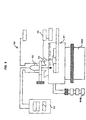
- the current dependency of luminescent intensity was measured on the luminescent device 1A according to the example of this invention and the conventional luminescent device 101A using an experimental equipment 50 shown in FIG. 3.
- the experimental equipment 50 is made up of a vacuum device 51 accommodating the samples (the luminescent devices) 1A and 101A being measured and placed internally in a substantial vacuum condition, an electron gun 52 for applying an electron beam to the samples measured in the vacuum device 51, a high-voltage power supply 53 for supplying high-voltage power to the electron gun 52, a sputter ion pump 54A and turbo-molecular pump 54B for making the interior of the vacuum device 51 vacuous (up to 1 x 10 -5 Pa), and an observation window or port 55 for observation of the interior of the vacuum device 51.
- the observation window 55 is also used as an entry through which an electron beam evaluation device 56 or a luminescent spectrometer (not shown) is inserted into the interior of the vacuum device 51.
- the sputter ion pump 54A and the turbo-molecular pump 54B are properly manipulated so that the interior of the vacuum device 51 forms a vacuum below a sufficient degree of vacuum (for example, 1 x 10 -5 Pa).
- the high-voltage power supply 53 is actuated to apply electron beam from the electron gun 52 to the luminescent device 1A and 101A in the interior of the vacuum device 51, and the current dependency of luminescent intensity of each of the luminescent device 1A and 101A is measured with the electron beam evaluation equipment 56.
- FIG. 4 is a log-log graph where the vertical axis represents luminescent intensity I of a luminescent device and the horizontal axis denotes beam current (current value) A fed to the electron gun 52 (that is, energy applied to the luminescent device 1A or 101A).
- the luminescent intensity I increased monotonically with increase in beam current A until the beam current A approaches approximately 30 ⁇ A, while the luminescent intensity I decreased when the beam current A exceeded 30 ⁇ A.
- the luminescent intensity I of this luminescent device 1A is denoted by circled numeral 2 in FIG. 4.
- the luminescent intensity I of this luminescent device 1A increased monotonically with an increase in the beam current A until the beam current A goes to the vicinity of the 20 ⁇ A just as the conventional luminescent device 101A does.
- the beam current A exceeded approximately 20 ⁇ A, the increase tendency thereof went upward rapidly so that the luminescent intensity increased superlinearly to reach an extremely high value. This result was contrary to the case of the conventional luminescent device 101A.
- the luminescent intensity I increases superlinearly when the beam current A exceeds a threshold A 0 (in this case, approximately 20 ⁇ A), and an output can be higher than that of the conventional luminescent device 101A.
- the luminescent intensity I of this luminescent device 1A is lower than that of the conventional luminescent device 101A. This is because the area of the luminescent unit 3 of the luminescent device 1A. including the grooves 4, is made to be equal to the area of the luminescent unit 103 of the conventional luminescent device 101A; the luminescent device 1A has a smaller luminescence area of the luminescent unit 3 than that of the conventional luminescent device 101A by area corresponding to the grooves 4.
- a luminescent device 1B (having grooves 4) according to the second example of the present invention and a luminescent device 101B with a conventional fabrication (having no grooves) were prepared.
- blue phosphor (SrHfO 3 :Tm) invented previously was used for the luminescent device 1B and 101B.
- the luminescent device 1B is made up of a copper-made substrate 2, a luminescent unit 3 and lattice-like grooves 4 as well as the above-mentioned luminescent device 1A according to the first example as shown in FIGs. 1(A) and 1(B).
- the luminescent unit 3 was made on the substrate 2 with the blue phosphor (SrHfO 3 :Tm) powder being settling-coated in water-glass aqueous solution.
- the luminescent device 101B is composed of a copper-made substrate 102 and a luminescent unit 103 formed by settling-coating blue phosphor (SrHfO 3 :Tm) powder onto the substrate 102 in water-glass aqueous solution.
- a luminescent unit 103 formed by settling-coating blue phosphor (SrHfO 3 :Tm) powder onto the substrate 102 in water-glass aqueous solution.
- the blue phosphor (SrHfO 3 :Tm) powder synthesis is feasible according to the methods disclosed in Japanese Patent Laid-Open Nos. HEI 8-283713, 10-121041 and 10-121043.
- the blue phosphor (SrHfO 3 :Tm) powder synthesis Sr (strontium) oxide, hydroxide, carbonate or nitrate, Hf (hafnium) oxide and others were weighed for a quantity and intermixed sufficiently, and in a heat resistance vessel such as a crucible, this mixture was fired once or more times at a temperature of 800 to 1600°C for one to twelve hours in air or in oxidation atmosphere.
- the blue phosphor powder synthesis was conducted as follows.
- the luminescent device 1B (the luminescent device 101B) was set in the equipment 50 shown in FIG. 3.
- the current dependency of luminescent intensity was measured on the luminescent device 1B and 101B with the electron beam evaluation equipment 56.
- the luminescent spectrum was measured by the luminescent spectrometer.
- FIG. 5 shows the results of measurement of the current dependency of luminescent intensity.
- FIG. 6 shows the results of measurement of luminescent spectrum.
- the luminescent spectrometer (not shown) is set in place of the electron beam evaluation equipment 56.
- the vertical axis represents luminescent intensity I of a luminescent device while the horizontal axis denotes a beam current A supplied to the electron gun 52 .
- the luminescent intensity I increased monotonically with an increase in the beam current A until the beam current A approaches approximately 30 ⁇ A.
- the increase tendency thereof went downward, and when the beam current A exceeds approximately 100 ⁇ A, the luminescent intensity I fell into a saturated condition.
- the luminescent intensity I increased monotonically until the beam current A increased up to approximately 100 ⁇ A.
- the increase tendency thereof went upward rapidly and the luminescent intensity I increased superlinearly.
- the luminescent intensity I increased superlinearly when the beam current A exceeded this threshold A 0 (in this case, approximately 100 ⁇ A) contrary to that of the conventional luminescent device 101A.
- FIG. 6 shows a luminescent spectrum of the luminescent device 1B in a case when a beam current A larger than the threshold A 0 is supplied to the electron gun 52; the horizontal axis represents a wavelength ⁇ [nm] of the luminescence and the vertical axis denotes a luminescent intensity I.
- the luminescent intensity I shows a peak (luminescent peak) S1 in the vicinity of 450 nm.
- This luminescent peak S1 corresponds to a blue luminescent band stemming from f-f transitions of Tm forming the luminescence center of a blue phosphor (SrHfO 3 :Tm) constituting the luminescent unit 3.
- SrHfO 3 :Tm blue phosphor
- the luminescent intensity I increases superlinearly and the luminescent color varies (in this case, varies from blue to white) when the beam current A exceeds the threshold A 0 .
- a luminescent device 1C was made up of a copper-made substrate 2, a luminescent unit 3 formed on the substrate 2 by the dusting of phosphor powder and lattice-like grooves 4 made in the luminescent unit 3 as shown in FIGs. 1(A) and 1(B); blue phosphor (SrHfO 3 : Tm) powder that contains KCl of 10 mol% acting as flux was used as the phosphor powder.
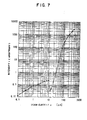
- FIG. 7 shows the current dependency of the luminescent intensity of the luminescent device 1C measured with the experimental equipment 50 shown in FIG. 3.
- the vertical axis represents luminescent intensity I of a luminescent device and the horizontal axis denotes beam current A to be supplied to the electron gun 52.
- the intensity I monotonically increased until the beam current increased up to threshold (about 10 ⁇ A).
- the luminescent intensity I once dropped when the beam current A exceeds the threshold A 0 .
- the luminescent intensity I increased superlinearly at an increase tendency greater than that below the threshold A 0 .
- the threshold A 0 is approximately 10 ⁇ A, which was a lower value than the thresholds A 0 of the luminescent devices 1A and 1B according to the above-described examples.
- the reason of the lower threshold A 0 can be assumed as follows.
- the above-mentioned superlinear rise of the luminescent intensity was observed when the energy applied to the luminescent device exceeded a threshold. This can be enhanced by electrification property of the luminescent unit 3.
- non-electrical conductive phosphor powder is employed for making the luminescent unit 3 acquire the electrification property
- water glass with electrical-conductive property is used as binder for the formation of the luminescent unit 3 on the substrate 2; therefore, the non-electrical conductive property of the luminescent unit 3 containing the water glass is impaired to somewhat diminish the electrification property thereof.
- ZnO has electrical conductive property (estimated electrical resistivity is 10 to 300 ⁇ cm) in the form of phosphor powder and put on the market.
- the phosphor powder ZnO was coated by sedimentation on a copper-made substrate 2 in water-glass aqueous solution and dried sufficiently to form powder layer (luminescent unit) 3 on the substrate 2.
- lattice-like grooves 4 were made in the powder layer 3 at an interval of 1 mm with a sharp-edged tool such as a pincette.
- phosphor powder ZnO was coated by sedimentation on a substrate 1 in water-glass aqueous solution and dried sufficiently to form powder layer (luminescent unit) 3 on the substrate 2, thereby producing a luminescent device 101D with conventional fabrication.
- the luminescent intensity under the bombardment of electron beam current was measured for these luminescent device 1D and 101D, through the use of the experimental equipment 50 shown in FIG. 3. The results are shown in FIG. 8.
- the vertical axis represents luminescent intensity I of the luminescent device and the horizontal axis denotes beam current A supplied to the electron gun 52.
- circled numeral 6 is for the luminescent device 1D (having grooves) and circled numeral 5 is for the luminescent device 101D (without grooves).
- the luminescent intensity I showed a maximum value in the vicinity of beam current A of 100 ⁇ A, and the luminescent intensity I decreased beyond the beam current A. This was irrespective of the presence (the luminescent device 1D) or absence (luminescent device 101D) of grooves. In case the luminescent unit was fabricated with an electrical conductive phosphor, the luminescent intensity I thus did not increase superlinearly even if the beam current A increased beyond a threshold. The effect of the grooves 4 was not obtained.
- the powder (phosphor) itself has electrical conductive property to acquire less electrification property even if the grooves 4 are made in the luminescent unit 3 so that the luminescent unit 3 has minute uneven surface for facilitating the storage of electric charge.
- the electrification property of the luminescent unit 3 is related to the above-mentioned phenomenon (the phenomenon that the luminescent intensity I increases superlinearly with the beam current A above a threshold, as observed in the three examples).
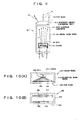
- FIG. 9 is an illustrative view showing a configuration of the image tube as the first application example of the structured lighting material according to the present invention.
- a face glass 62 is fixedly adhered onto a cylindrical glass vessel 61 to produce a vacuum vessel (envelop) 63 in this image tube.
- a vacuum vessel (envelop) 63 in this image tube.
- a luminescent surface (luminescent unit) 64 in the interior of the vacuum vessel (envelope) 63, there are a luminescent surface (luminescent unit) 64, an anode electrode (substrate) 65 and a cathode forming a electron discharge unit (a grid 66, a cathode 67).
- a structured lighting material according to the present invention is applied to the aforesaid luminescent surface 64 and anode electrode 65.
- the anode electrode 65 is composed of a metallic electrode made of aluminum, copper or the like, or a metal plated electrode made of these metals.
- the cathode 67 of the electron discharge section is typically a conventional filament (for example, made by applying electron-emissive material like barium oxide/calcium oxide/strontium oxide to the tungsten filament), carbon nanotube or the like.
- a voltage is applied to the grid 66 to establish a condition of electron discharge from the electrode 67.
- a electric potential works on the anode electrode 65 and the electrons discharged from the cathode 67 are accelerated to collide against and penetrate the anode electrode 65, thereby making impact on the luminescent surface 64.
- the luminescent surface 64 is excited by the electron impact and luminescent color corresponding to the luminescent material forming the luminescent surface 64 passes through the face glass 62 and appears as luminescence 68 on the front side.
- FIG. 10 is an illustrative view showing a configuration of a cathode-ray luminescent lamp as the second example of the application of a structured lighting material according to the present invention.
- a vacuum vessel (envelope) 63A is composed of a cylindrical glass vessel 61A and a face glass 62A.
- a luminescent surface (luminescent unit) 64A in the interior of the vacuum vessel (envelope) 63A, there are a luminescent surface (luminescent unit) 64A, an anode electrode (substrate) 65A and a cathode forming a electron discharge section (a grid 66A, a cathode 67A).
- a structured lighting material according to the present invention is incorporated into the aforesaid luminescent surface 64A and anode electrode 65A.
- the anode electrode 65A is composed of a metallic electrode made of aluminum, copper or the like, or a metal plated electrode made of these metals.
- the cathode 67A of the electron discharge section is typically a conventional filament (for example, made by applying electron-emissive material like barium oxide/calcium oxide/strontium oxide to a tungsten filament), a carbon nanotube or the like.
- a voltage is applied to the grid 66A to make a condition of electron discharge from the electrode 67A.
- a electric potential works on the anode electrode 65A and the electrons discharged from the cathode 67A are accelerated toward the anode electrode 65A to collide against the luminescent surface 64A so that an impact takes place thereon.
- the luminescent surface 64A is excited by the electron impact and luminescent color corresponding to the luminescent material forming the luminescent surface 64A passes through the face glass 62A and luminescence takes place toward the front side.
- the luminescent surfaces 64 and 64A are made up of the structured lighting material with an uneven surface of luminescent unit.
- the configuration of the structured lighting material specifically the formation of the minute uneven surface of the luminescent unit (coated layer), realizes a high-efficient illuminator such as an image tube or a cathode-ray luminescent lamp.
Landscapes
- Luminescent Compositions (AREA)
- Investigating, Analyzing Materials By Fluorescence Or Luminescence (AREA)
Abstract
Description
Claims (18)
- A structured lighting material characterised by comprising a luminescent unit (3) wherein the intensity of its incoherent luminescence increases superlinearly when energy applied in a non-contact manner exceeds a threshold.
- A structured lighting material according to claim 1, characterised in that the luminescent color of said luminescent unit (3) changes when said energy exceeds said threshold.
- A structured lighting material according to claim 1, characterised in that said energy is electric energy originating from any one of electron beam, electric charge and electric field.
- A structured lighting material according to claim 1, characterised in that said luminescent unit (3) has non-electrical conductive property.
- A structured lighting material characterised by comprising a luminescent unit (3) which shows non-electrical conductive property and has a minute uneven surface, of which luminescent intensity increases superlinearly when energy applied to said minute uneven surface in a non-contact manner exceeds a threshold.
- A structured lighting material according to claim 5, characterised in that said minute uneven surface is formed in a manner that said luminescent unit (3) is formed to be non-uniform in thickness.
- A structured lighting material according to claim 6, characterised in that said minute uneven surface has high and low portions respectively corresponding to maximum and minimum thicknesses of said luminescent unit (3), and said maximum thickness is set to be three or more times said minimum thickness.
- A structured lighting material according to claim 6, characterised in that said minute uneven surface has high and low portions respectively corresponding to maximum and minimum thicknesses of said luminescent unit (3), and said maximum thickness is set to be ten or more times said minimum thickness.
- A structured lighting material according to claim 6, characterised in that said minimum thickness of said luminescent unit (3) is not more than 500 µm.
- A structured lighting material according to claim 6, characterised in that said minimum thickness of said luminescent unit (3) is not more than 50 µm.
- A structured lighting material according to claim 6, characterised in that an inclination angle α of the minute uneven surface is in a range from 30 degrees to 150 degrees.
- A structured lighting material according to claim 6, characterised in that an inclination angle α of the minute uneven surface is in a range from 50 degrees to 130 degrees.
- A structured lighting material according to claim 1, characterised in that said luminescent unit (3) is made of inorganic material.
- A structured lighting material according to claim 1, characterised in that said luminescent unit (3) is adhered on a substrate (2).
- A structured lighting material according to claim 14, characterised in that said luminescent unit (3) is adhered on said substrate (2) without water-soluble fixing agent.
- A structured lighting material according to claim 15, characterised in that said luminescent unit (3) is adhered on said substrate (2) in a manner of facilitating electrification.
- An illuminator characterised by comprising said structured lighting material defined in claim 1 or 5.
- A method to generate incoherent luminescence of which the luminescent intensity increases superlinearly when applied energy in a non-contact manner exceeds a threshold.
Applications Claiming Priority (2)
| Application Number | Priority Date | Filing Date | Title |
|---|---|---|---|
| JP2000397494 | 2000-12-27 | ||
| JP2000397494 | 2000-12-27 |
Publications (2)
| Publication Number | Publication Date |
|---|---|
| EP1220261A2 true EP1220261A2 (en) | 2002-07-03 |
| EP1220261A3 EP1220261A3 (en) | 2002-07-10 |
Family
ID=18862611
Family Applications (1)
| Application Number | Title | Priority Date | Filing Date |
|---|---|---|---|
| EP01130916A Withdrawn EP1220261A3 (en) | 2000-12-27 | 2001-12-27 | Structured lighting material, method to generate incoherent luminescence and illuminator |
Country Status (3)
| Country | Link |
|---|---|
| US (1) | US6683409B2 (en) |
| EP (1) | EP1220261A3 (en) |
| CN (1) | CN100339938C (en) |
Families Citing this family (5)
| Publication number | Priority date | Publication date | Assignee | Title |
|---|---|---|---|---|
| US7854861B2 (en) * | 2001-10-19 | 2010-12-21 | Applied Nanotech Holdings, Inc. | Well formation |
| CN1849687B (en) * | 2003-09-12 | 2010-07-14 | 毫微-专卖股份有限公司 | Formation of grooves |
| JP4553596B2 (en) * | 2004-01-29 | 2010-09-29 | 三菱レイヨン株式会社 | Light guide for surface light source device, method for manufacturing the same, and surface light source device |
| US20060275563A1 (en) * | 2005-06-06 | 2006-12-07 | Kevin Duffy | Biodegradable and compostable material |
| DE102010063756A1 (en) * | 2010-12-21 | 2012-06-21 | Osram Ag | Production of phosphor layers using alkali metal silicates |
Family Cites Families (6)
| Publication number | Priority date | Publication date | Assignee | Title |
|---|---|---|---|---|
| NL6903366A (en) * | 1969-03-05 | 1970-09-08 | ||
| JPS6235447A (en) | 1985-08-07 | 1987-02-16 | Mitsubishi Electric Corp | Multicolor display cathode-ray tube |
| US5637958A (en) * | 1995-03-06 | 1997-06-10 | Texas Instruments Incorporated | Grooved anode plate for cathodoluminescent display device |
| JP3475565B2 (en) | 1995-04-17 | 2003-12-08 | 三菱化学株式会社 | Phosphor |
| JPH10121043A (en) | 1996-10-15 | 1998-05-12 | Mitsubishi Chem Corp | Phosphor |
| JPH10121041A (en) | 1996-10-15 | 1998-05-12 | Mitsubishi Chem Corp | Video display tube |
-
2001
- 2001-12-27 EP EP01130916A patent/EP1220261A3/en not_active Withdrawn
- 2001-12-27 US US10/033,047 patent/US6683409B2/en not_active Expired - Fee Related
- 2001-12-27 CN CNB011439572A patent/CN100339938C/en not_active Expired - Fee Related
Also Published As
| Publication number | Publication date |
|---|---|
| US6683409B2 (en) | 2004-01-27 |
| CN1362591A (en) | 2002-08-07 |
| EP1220261A3 (en) | 2002-07-10 |
| CN100339938C (en) | 2007-09-26 |
| US20020079824A1 (en) | 2002-06-27 |
Similar Documents
| Publication | Publication Date | Title |
|---|---|---|
| US6559598B2 (en) | Plasma picture screen with UV light emitting layer | |
| US6819041B2 (en) | Luminescence crystal particle, luminescence crystal particle composition, display panel and flat-panel display | |
| US7683530B2 (en) | Cathodoluminescent light source having an electron field emitter coated with nanocarbon film material | |
| WO1996014206A1 (en) | Semiconductor nanocrystal display materials and display apparatus employing same | |
| JP2002265942A (en) | Phosphor powder, manufacturing method thereof, display panel, and flat display device | |
| KR970706370A (en) | Phosphor, and cathode ray tube and display device using the phosphor and display device | |
| US20020140338A1 (en) | Luminous low excitation voltage phosphor display structure deposition | |
| US6069439A (en) | Phosphor material, method of manufacturing the same and display device | |
| US6683409B2 (en) | Structured lighting material, method to generate incoherent luminescence and illuminator | |
| EP1580799A2 (en) | Lighting device | |
| US7541733B2 (en) | Light-emitting element, method for producing the same and display device | |
| JP3965298B2 (en) | LIGHT EMITTING STRUCTURE, LIGHT EMITTING METHOD, AND LIGHTING BODY | |
| JP2007242624A (en) | LIGHT EMITTING STRUCTURE, LIGHT EMITTING METHOD, AND LIGHTING BODY | |
| US5611719A (en) | Method for improving flat panel display anode plate phosphor efficiency | |
| JP2003020476A (en) | Phosphor thin film, thin film electroluminescence display device, field emission display device, and method of forming phosphor thin film | |
| US5593562A (en) | Method for improving flat panel display anode plate phosphor efficiency | |
| US20090072701A1 (en) | Luminescent screen | |
| KR19980032935A (en) | Field emission display | |
| US5838118A (en) | Display apparatus with coated phosphor, and method of making same | |
| JP3417831B2 (en) | Manufacturing method of phosphor material | |
| JP5600590B2 (en) | Power-saving high-intensity integrated fluorescent lamp | |
| KR100187484B1 (en) | Electron beam excitation phosphor | |
| JP2904106B2 (en) | Phosphor | |
| JP2795185B2 (en) | Display device | |
| CN1347957A (en) | Illuminating material and producing process and display substrate and display device containing the same illuminating material |
Legal Events
| Date | Code | Title | Description |
|---|---|---|---|
| PUAI | Public reference made under article 153(3) epc to a published international application that has entered the european phase |
Free format text: ORIGINAL CODE: 0009012 |
|
| PUAL | Search report despatched |
Free format text: ORIGINAL CODE: 0009013 |
|
| AK | Designated contracting states |
Kind code of ref document: A2 Designated state(s): AT BE CH CY DE DK ES FI FR GB GR IE IT LI LU MC NL PT SE TR |
|
| AX | Request for extension of the european patent |
Free format text: AL;LT;LV;MK;RO;SI |
|
| AK | Designated contracting states |
Kind code of ref document: A3 Designated state(s): AT BE CH CY DE DK ES FI FR GB GR IE IT LI LU MC NL PT SE TR |
|
| AX | Request for extension of the european patent |
Free format text: AL;LT;LV;MK;RO;SI |
|
| 17P | Request for examination filed |
Effective date: 20020724 |
|
| AKX | Designation fees paid |
Designated state(s): DE |
|
| 17Q | First examination report despatched |
Effective date: 20031001 |
|
| RAP1 | Party data changed (applicant data changed or rights of an application transferred) |
Owner name: MITSUBISHI CHEMICAL CORPORATION |
|
| RAP1 | Party data changed (applicant data changed or rights of an application transferred) |
Owner name: MITSUBISHI CHEMICAL CORPORATION |
|
| STAA | Information on the status of an ep patent application or granted ep patent |
Free format text: STATUS: THE APPLICATION HAS BEEN WITHDRAWN |
|
| 18W | Application withdrawn |
Effective date: 20090804 |