EP1220231A2 - Circuit and method for performing a stress test on a ferroelectric memory device - Google Patents
Circuit and method for performing a stress test on a ferroelectric memory device Download PDFInfo
- Publication number
- EP1220231A2 EP1220231A2 EP01309870A EP01309870A EP1220231A2 EP 1220231 A2 EP1220231 A2 EP 1220231A2 EP 01309870 A EP01309870 A EP 01309870A EP 01309870 A EP01309870 A EP 01309870A EP 1220231 A2 EP1220231 A2 EP 1220231A2
- Authority
- EP
- European Patent Office
- Prior art keywords
- lines
- row
- memory cells
- column
- line
- Prior art date
- Legal status (The legal status is an assumption and is not a legal conclusion. Google has not performed a legal analysis and makes no representation as to the accuracy of the status listed.)
- Withdrawn
Links
Images


Classifications
-
- G—PHYSICS
- G11—INFORMATION STORAGE
- G11C—STATIC STORES
- G11C29/00—Checking stores for correct operation ; Subsequent repair; Testing stores during standby or offline operation
- G11C29/04—Detection or location of defective memory elements, e.g. cell constructio details, timing of test signals
- G11C29/50—Marginal testing, e.g. race, voltage or current testing
-
- G—PHYSICS
- G11—INFORMATION STORAGE
- G11C—STATIC STORES
- G11C11/00—Digital stores characterised by the use of particular electric or magnetic storage elements; Storage elements therefor
- G11C11/21—Digital stores characterised by the use of particular electric or magnetic storage elements; Storage elements therefor using electric elements
- G11C11/22—Digital stores characterised by the use of particular electric or magnetic storage elements; Storage elements therefor using electric elements using ferroelectric elements
Definitions
- the present invention relates to testing a ferroelectric memory device, and particularly to performing a stress test on a ferroelectric memory device.
- Ferroelectricity is a phenomenon which can be observed in a relatively small class of dielectrics called ferroelectric materials.
- a normal dielectric upon the application of an electric field, positive and negative charges will be displaced from their original position - a concept which is characterized by the dipole moment or polarization. This polarization or displacement will vanish, however, when the electric field returns back to zero.
- a spontaneous polarization - a displacement which is inherent to the crystal structure of the material and does not disappear in the absence of the electric field.
- the direction of this polarization can be reversed or reoriented by applying an appropriate electric field.
- ferroelectric capacitors formed from ferroelectric film or material disposed between parallel conduction plates, being capable of storing in a nonvolatile manner a first charge corresponding to a first polarization state in which the direction of polarization is in a first direction, and a second charge corresponding to a second polarization state in which the direction of polarization is in a second direction opposite the first direction.
- Ferroelectric capacitors are utilized in nonvolatile random access memory devices having a memory cell array architecture that is similar to the memory cell array architecture of dynamic random access memory (DRAM) devices.
- DRAM dynamic random access memory
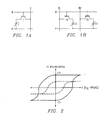
- a one transistor, one capacitor (1T1C) memory cell utilizes a pass gate transistor T connected between a column line B and a first plate of ferroelectric capacitor C.
- a second plate of ferroelectric capacitor C is connected to a plate line P.
- the gate terminal of pass gate transistor T is connected to a word line W.
- a memory device utilizing a 1T1C memory cell uses a reference memory cell that is accessed at the same time the 1T1C memory cell is accessed so as to provide a charge differential appearing across a pair of column lines coupled to the 1T1C cell and the reference cell.
- the use of 1T1C ferroelectric memory cells is known in the art.
- a two transistor, two capacitor (2T2C) memory cell includes two ferroelectric capacitors C1 and C2.
- a first pass gate transistor T1 is connected between a first plate of ferroelectric capacitor C1 and a first column line BL of a column line pair.
- a second pass gate transistor T2 is connected between a first plate of ferroelectric capacitor C2 and a second column line BL' of the column line pair.
- a second plate of ferroelectric capacitors C1 and C2 is connected to a plate line P.
- the gate terminal of pass gate transistors T1 and T2 is connected to the word line W.
- Each capacitor C1 and C2 stores a charge representative of the polarization state thereof, the charge combining with the charge of the other capacitor to result in a charge differential appearing across column lines BL and BL' when the 2T2C memory cell is accessed.
- the polarity of the charge differential denotes the binary value stored by the 2T2C memory cell.
- Imprint is a characteristic of ferroelectric films that refers to the tendency of a ferroelectric film/capacitor to prefer one polarization state over another polarization state. Imprint is known to occur when a ferroelectric capacitor is maintained in a single polarization state for a prolonged period of time. Imprint adversely effects the ability of a ferroelectric capacitor to switch between the polarization states. Consequently, the existence of imprint may directly impact the performance of a ferroelectric memory device.
- ferroelectric memory cells The performance of ferroelectric memory cells has been seen to degrade over time due to a number of other phenomena as well. For instance, ferroelectric memory cells may be effected by fatigue, retaining data over time, etc. When holding data over a prolonged period of time, such as under accelerated conditions during burn-in, a ferroelectric memory cell may be seen to degrade over the course of several hours or days.
- Figure 2 shows how a ferroelectric memory cell may be degraded, with the polarization characteristic being shown for a normal ferroelectric memory cell in continuous set of lines and the polarization characteristic being shown for a degraded ferroelectric memory cell in dashed lines.
- Stress testing of integrated circuits, such as memory devices, is typically accomplished by applying an overvoltage to the gates of the transistors in the memory array. For example, testing on a memory device rated at five volts may be performed at nine volts. To perform this test, it is common to activate multiple wordlines and columns on a simultaneous basis thus applying the testing overvoltage at each memory cell within the memory array. Defective columns and rows may then be detected. The defective portions of the device are then replaced using built-in redundancy features, or the device is discarded as defective.
- a ferroelectric memory device includes a memory array of memory cells organized into rows and columns, with each row of memory cells being coupled to a word line and a plate line and each column of memory cells being coupled to a bit line.
- the ferroelectric memory device further includes address decode circuitry for receiving an address value and asserting a signal appearing on at least one row line to connect at least one row of memory cells to the column lines.
- the ferroelectric memory device includes test circuitry for receiving at least one test control signal and in response to the at least one test control signal allowing a voltage differential to be applied between the column lines and the plate lines, so that a stress voltage may be applied across the ferroelectric capacitor of each of the memory cells.
- the operation of the ferroelectric memory device in performing a stress test includes connecting each row of memory cells to the column lines and applying a stress voltage between the column lines and the plate lines for a predetermined period of time. In this way, the dielectric material of the capacitor of each memory cell is stressed at elevated voltages for detecting weak oxides, thin oxides, particle defects, etc. in the memory cells.
- Memory device 1 is a nonvolatile memory device, such as a random access ferroelectric memory device. It is understood, however, that memory device 1 may be other memory devices as well. For instance, memory device 1 may include memory cells having elements other than ferroelectric capacitive elements that may provided a degraded performance over time.
- memory device 1 may itself form an integrated circuit or be a memory device that is embedded with other circuitry within an integrated circuit.
- Memory device 1 includes a memory cell array 2 of memory cells 3.
- Memory cells 3 may be ferroelectric memory cells that include one or more ferroelectric capacitor elements C.
- Memory cell 3 may be implemented as a one transistor, one capacitor (1T1C) memory cell ( Figure 1A).
- memory cell 3 may be implemented as a two transistor, two capacitor (2T2C) memory cell ( Figure 1B).
- each memory cell 3 may be implemented in other ways using one or more ferroelectric capacitive elements or similar elements.
- Memory cell array 2 is arranged into rows and columns of memory cells 3.
- the memory cells 3 in a row of memory cells 3 are connected to a distinct word line 7 and a distinct plate line 8.
- the memory cells 3 in a column of memory cells 3 are connected to a distinct column line 6 or pair 5 thereof.
- Figure 3 shows plate lines 8 being parallel to word lines 7.
- plate lines 8 can be coupled to more than one row of memory cells 3.
- plate lines 8 may be perpendicular to word lines 7.
- the voltage appearing across the ferroelectric capacitors in the memory cells 3 in rows that are not being accessed will not vary when the plate line 8 connected to such memory cells 3 is asserted. This is due to the fact that the transistor(s) in the unaccessed memory cells 3 are turned off, so the plate connected to the transistor simply follows the voltage change appearing on the capacitor plate connected to the asserted plate line 8.
- back plate lines 8 may be partitioned into smaller segments so that back plate lines 8 may be more easily driven.
- Memory device 1 may include an address input buffer 15 which receives the address value provided to memory device 1 and generates a true and a complement version of the address value.
- the true version, output signal OUTt, and the complement version, output signal OUTc may be generated by address input buffer 15 with necessary timing so as to substantially prevent a false address selection.
- Memory device 1 further includes address logic, such as a row decoder circuit 9A, which receives and decodes true output signal OUTt and complement output signal OUTc from address input buffer 15.
- Row decoder circuit 9A generates a plurality of decoded output signals 90. In a normal mode of operation, output signals 90 identify a single row line 7 to be driven so as to connect the corresponding row of memory cells 3 to column lines 6.
- Row decoder circuit 9A may be implemented with combination logic so as to receive the true and complement versions of the address value.
- Memory device 1 further includes a column decoder circuit 9B, which also receives and decodes true output signal OUTt and complement output signal OUTc from address input buffer 15. Based upon the decoded signals OUTt and OUTc, column decoder circuit 9B couples one or more column lines 6 to data input/output bus 12.
- Memory device 1 includes a charge pump circuit 16 for boosting the row line 7 selected by row decode circuit 9A to an elevated or boosted voltage level.
- Charge pump circuit 16 ensures that the charge stored by memory cells 3 is fully shared with the corresponding column lines 6 during a memory read operation and that the capacitor C in each selected memory cell 3 is driven to the high reference voltage level Vdd during a memory write operation.
- row line control circuit 17 receives the decoded output signal 90 from row decode circuit 9A and the output of charge pump circuit 16, and in response drives the row line 7 identified by row decode circuit 9A to the boosted voltage level.
- Sense amplifiers 10 are controlled to sense a charge differential appearing across a pair of column lines 6 and drive the column lines 6 to the high voltage reference Vdd and low voltage reference Vss based upon the polarity of the charge differential.
- Input/output (I/O) block 11 serves as an interface between column lines 6 and the external data input/output bus 12.
- a control circuit 13 provides necessary timing and control signals to memory cell array 2, address logic 9A and 9B, sense amplifiers 10 and data input/output block 11 to preform read and write memory access operations.
- Memory device 1 is shown in Figure 3 as having a bidirectional external data bus 12. It is understood that memory device 1 may include separate unidirectional data input and data output buses instead.
- memory device 1 includes test circuitry.
- the test circuitry configures memory device 1 for effectively stressing the dielectrics therein (i.e., the dielectrics in ferroelectric capacitors C and the gate transistor dielectrics) by stressing the dielectrics in parallel. In this way, weak dielectrics, undesirably thin dielectrics and particle defects in memory device 1 may be efficiently identified.
- test mode signal TEST is received by the address input buffer 15 such that when test mode signal TEST is asserted, both the true output signals OUTt and the complement output signals OUTc of address input buffer 15 are asserted.
- This causes row decode circuit 9A to assert and/or drive each decoded output signal 90 that is input to row line control circuit 17 so as to indicate that memory cells 3 of each row 7 should be connected to column lines 6.
- Row line control circuit 17 responsively allows each row line 7 to be driven to a high voltage level to connect memory cells in each row to column lines 6.
- Figure 4 is a schematic of a single bit slice of the address input buffer 15 according to an embodiment of the present invention. It is understood that the bit slice is replicated once for each bit of the address input buffer 15.
- address input buffer 15 utilizes a first signal path 91 for generating the true output signal OUTt and a second signal path 92 for generating the complement output signal OUTc.
- Each of the first and second signal paths includes series connected delay elements 93 which provide different propagation delay times between a falling edge transition and a rising edge transition. In this way, address input buffer 15 provides input glitch tolerance and prevents false address selection with output signal deassertion prior to one of true output signal OUTt and complement output signal OUTc being asserted.
- An edge transition detection (ETD) circuit 94 receives the true output signal OUTt and the complement output signal OUTc and generates an ETD output signal which is connected in a wired-NOR configuration with the ETD output signal of each bit slide of the address input buffer 15.
- Address input buffer 15 is described in greater detail in U.S. Patent Application 183,593, entitled “DEVICE AND METHOD FOR ADDRESS INPUT BUFFERING", filed 10/30/98, which is incorporated by reference herein in its entirety.
- test mode signal TEST is applied as an input to both the first and second signal paths of address input buffer 15. As can be seen, asserting test mode signal TEST to a logic high state asserts both the true output signal OUTt and complement output signal OUTc, which forces address decode logic circuit 9 to assert each output thereof so that row line control circuit 17 is configured to drive each row line 7 of memory device 1 to the same voltage level simultaneously.
- the test circuitry of memory device 1 includes a multiplexer circuit 20 that receives test mode signal TEST and responsively selects one of the output of charge pump circuit 16 and external signal Row-Ext for application to row control circuit 17 and therefore to row lines 7.
- multiplexer circuit 20 connects external signal Row-Ext to row control circuit 17.
- External signal Row-Ext is connected to a pad (not shown) on the integrated circuit in which memory device 1 is formed, so that external signal Row-Ext may receive a voltage level that is applied from a device, such as a tester, that is external to the integrated circuit.
- the pad to which external signal Row-Ext is connected may be optionally connected to a package pin when the integrated circuit is packaged.
- a pull-down device may be used to pull external signal Row-Ext to the ground potential in an absence of a voltage being applied thereto.
- a pull-down device may be used to pull test mode control signal TEST to the ground potential in an absence of a voltage being applied thereto.
- test circuitry of memory device 1 includes multiplexer circuitry 21 that receives test mode signal TEST and responsively selects either one of external signal Plate-Ext and the drive signal 23 that is used to drive plate lines 8 during the normal mode of operation.
- External signal Plate-Ext is connected to a pad (not shown) on the integrated circuit so that a device external to the integrated circuit, such as a tester, may drive external signal Plate-Ext.
- test circuitry may further include a noninverting gate 24 that connects an external signal Col-Ext to column lines 6 when test mode signal TEST is asserted, and disconnects external signal Col-Ext from column lines 6 when test mode signal TEST is deasserted.
- a noninverting gate 24 that connects an external signal Col-Ext to column lines 6 when test mode signal TEST is asserted, and disconnects external signal Col-Ext from column lines 6 when test mode signal TEST is deasserted.
- an elevated voltage differential may be applied between column lines 6 and plate lines 8 by driving one of external signals Plate-Ext and Col-Ext to an elevated voltage and the other to a ground potential.
- test mode signal TEST is asserted, external signals Row-Ext and Plate-Ext are driven to an elevated voltage and external signal Col-Ext is driven to a lower voltage, such as the ground potential.
- memory device 1 is powered up. With test mode signal TEST being asserted, memory device 1 is powered up into the test mode.
- Address input buffer 15 asserts output signals OUTt and OUTc so that row decode circuit 9A indicates to row control circuit 17 that each row line 7 is to be connected to external signal Row-Ext.
- each memory cell 3 being connected to the column lines 6, and with an elevated voltage differential applied across column lines 6 and plate lines 8, the dielectrics in memory cells 3 are stressed under an electric field applied in a first direction.
- memory device 1 may be powered down.
- test mode signal TEST is maintained in the asserted state, external signals Row-Ext and Col-Ext are driven to an elevated voltage and external signal Plate-Ext driven to a lower voltage level, such as the ground potential.
- Memory device 1 is then powered up in the stress test mode. With each memory cell 3 being connected to the column lines 6, and with an elevated voltage differential applied across column lines 6 and plate lines 8, the dielectrics in memory cells 3 are stressed under an electric field applied in a second direction opposite the first direction.
Abstract
Description
Claims (17)
- A ferroelectric memory device, comprising:a memory array of memory cells organized into rows and columns, including a plurality of word lines, plate lines and bit lines, each row of memory cells being coupled to a word line and a plate line and each column of memory cells being coupled to a bit line, each memory cell comprising at least one ferroelectric capacitor and at least one transmission gate transistor connected thereto;address decode circuitry for receiving an address value and asserting a signal appearing on at least one row line to connect at least one row of memory cells to the column lines; andtest circuitry for receiving at least one test control signal and in response to the at least one test control signal allowing a voltage differential to be applied between the column lines and the plate lines, so that a stress voltage may be applied across the at least one ferroelectric capacitor of the memory cells.
- The memory device of claim 1, further comprising:a multiplexor circuit connected between one of the plate lines and the column lines, for selectively connecting an external signal to one of the plate lines and the column lines based upon the value of the at least one test control signal.
- A method of testing a ferroelectric memory device having a plurality of memory cells arranged into rows and columns, with each row of memory cells being connected to a row line and a plate line and each column of memory cells being connected to a column line, comprising:connecting each row of memory cells to the column lines; andapplying a stress voltage between the column lines and the plate lines for a predetermined period of time.
- The method of claim 3, wherein the connecting of each row of memory cells to the column lines occurs at power up of the ferroelectric memory device.
- The method of claim 3, wherein the connecting of each row of memory cells to the column lines comprises applying an externally generated voltage to the row lines.
- The method of claim 3, wherein the connecting of each row of memory cells comprises decoupling the row lines from a charge pump circuit.
- The method of claim 3, wherein the applying a stress voltage comprises applying the stress voltage of a first polarity between the column lines and the plate lines for a first predetermined period of time and applying a stress voltage of a second polarity, opposite the first polarity, between the column lines and the plate lines for a second predetermined period of time.
- The method of claim 3, further comprising placing transistors in the ferroelectric memory device in a linear mode of operation prior to the step of applying a stress voltage.
- An integrated circuit, comprising:a memory device, comprising:a memory array of memory cells organized into rows and columns, including a plurality of word lines, plate lines and bit lines, each row of memory cells being coupled to a word line and a plate line and each column of memory cells being coupled to a bit line, each memory cell comprising at least one capacitor and at least one transmission gate transistor connected in series between a plate line and a column line;address decode circuitry for receiving an address value and asserting a signal appearing on at least one row line to connect at least one row of memory cells to the column lines; andtest circuitry for receiving at least one test control signal and in response to the at least one test control signal allowing a stress voltage differential to be applied across the column lines and the plate lines.
- The integrated circuit of claim 9 or device of claim 1, wherein the address decode circuitry is responsive to the at least one test control signal to selectively assert a signal on each row line so as to connect each row of memory cells to the column lines at one time.
- The integrated circuit of claim 9 or device of claim 1, wherein the address decode circuitry is responsive to the at least one test control signal to selectively assert a signal on each row line so as to connect each row of memory cells to the column lines during power up of the ferroelectric memory device.
- The integrated circuit of claim 9 or device of claim 1, further comprising:an address input buffer circuit for storing the received address value and providing the stored address value to the address decode circuitry on a plurality of true and complement output signals, the address input buffer is responsive to the at least one test control signal to assert each true and complement output signal of the address input buffer circuit.
- The integrated circuit of claim 9 or device of claim 1, further comprising:wherein the test circuitry is selectively disconnected from the row lines based upon the value of the at least one test control signal.charge pump circuitry coupled to the row lines, for generating a voltage level on the row lines in excess of a high reference voltage level;
- The integrated circuit or device of claim 13, wherein the test circuitry includes a multiplexing circuit connected between the charge pump circuitry and the row lines, the at least one test control signal driving a selection input of the multiplexing circuit.
- The integrated circuit or device of claim 14, wherein
a pad disposed on the integrated circuit is connected to an input of the multiplexing circuit so that the row lines are coupled to either of an output of the charge pump circuitry and the pad. - The integrated circuit or device of claim 15, further comprising row line control circuitry connected between the multiplexing circuit and the row lines.
- The integrated circuit of claim 9, wherein the memory device is embedded within the integrated circuit.
Applications Claiming Priority (2)
| Application Number | Priority Date | Filing Date | Title |
|---|---|---|---|
| US751007 | 2000-12-29 | ||
| US09/751,007 US6359819B1 (en) | 2000-12-29 | 2000-12-29 | Circuit and method for performing a stress test on a ferroelectric memory device |
Publications (2)
| Publication Number | Publication Date |
|---|---|
| EP1220231A2 true EP1220231A2 (en) | 2002-07-03 |
| EP1220231A3 EP1220231A3 (en) | 2003-03-12 |
Family
ID=25020063
Family Applications (1)
| Application Number | Title | Priority Date | Filing Date |
|---|---|---|---|
| EP01309870A Withdrawn EP1220231A3 (en) | 2000-12-29 | 2001-11-23 | Circuit and method for performing a stress test on a ferroelectric memory device |
Country Status (2)
| Country | Link |
|---|---|
| US (1) | US6359819B1 (en) |
| EP (1) | EP1220231A3 (en) |
Families Citing this family (5)
| Publication number | Priority date | Publication date | Assignee | Title |
|---|---|---|---|---|
| JP2001351373A (en) * | 2000-06-07 | 2001-12-21 | Matsushita Electric Ind Co Ltd | Semiconductor memory and semiconductor integrated circuit using it |
| US6584007B2 (en) * | 2000-12-29 | 2003-06-24 | Stmicroelectronics, Inc. | Circuit and method for testing a ferroelectric memory device |
| US6754094B2 (en) * | 2002-01-31 | 2004-06-22 | Stmicroelectronics, Inc. | Circuit and method for testing a ferroelectric memory device |
| KR100484254B1 (en) * | 2002-10-31 | 2005-04-22 | 주식회사 하이닉스반도체 | Redundancy circuit in semiconductor memory device and fail repair method using the same |
| CN104934072B (en) * | 2015-05-12 | 2017-12-05 | 工业和信息化部电子第五研究所 | Single particle effect detection method and system |
Citations (4)
| Publication number | Priority date | Publication date | Assignee | Title |
|---|---|---|---|---|
| US5282167A (en) * | 1990-12-27 | 1994-01-25 | Kabushiki Kaisha Toshiba | Dynamic random access memory |
| US5852581A (en) * | 1996-06-13 | 1998-12-22 | Micron Technology, Inc. | Method of stress testing memory integrated circuits |
| US6046926A (en) * | 1997-10-15 | 2000-04-04 | Kabushiki Kaisha Toshiba | Ferroelectric memory and screening method therefor |
| US6055200A (en) * | 1998-11-07 | 2000-04-25 | Samsung Electronics Co., Ltd. | Variable test voltage circuits and methods for ferroelectric memory devices |
Family Cites Families (2)
| Publication number | Priority date | Publication date | Assignee | Title |
|---|---|---|---|---|
| SG79200A1 (en) * | 1995-08-21 | 2001-03-20 | Matsushita Electric Ind Co Ltd | Ferroelectric memory devices and method for testing them |
| US5661730A (en) * | 1996-09-27 | 1997-08-26 | Ramtron International Corporation | Same state and opposite state diagnostic test for ferroelectric memories |
-
2000
- 2000-12-29 US US09/751,007 patent/US6359819B1/en not_active Expired - Lifetime
-
2001
- 2001-11-23 EP EP01309870A patent/EP1220231A3/en not_active Withdrawn
Patent Citations (4)
| Publication number | Priority date | Publication date | Assignee | Title |
|---|---|---|---|---|
| US5282167A (en) * | 1990-12-27 | 1994-01-25 | Kabushiki Kaisha Toshiba | Dynamic random access memory |
| US5852581A (en) * | 1996-06-13 | 1998-12-22 | Micron Technology, Inc. | Method of stress testing memory integrated circuits |
| US6046926A (en) * | 1997-10-15 | 2000-04-04 | Kabushiki Kaisha Toshiba | Ferroelectric memory and screening method therefor |
| US6055200A (en) * | 1998-11-07 | 2000-04-25 | Samsung Electronics Co., Ltd. | Variable test voltage circuits and methods for ferroelectric memory devices |
Also Published As
| Publication number | Publication date |
|---|---|
| EP1220231A3 (en) | 2003-03-12 |
| US6359819B1 (en) | 2002-03-19 |
Similar Documents
| Publication | Publication Date | Title |
|---|---|---|
| US8472236B2 (en) | Differential plate line screen test for ferroelectric latch circuits | |
| US6714065B2 (en) | Semiconductor device including power supply circuit conducting charge pumping operation | |
| US20030185041A1 (en) | Semiconductor memory device | |
| EP2988305B1 (en) | Integrated circuit for storing data | |
| JPH04232693A (en) | Static type semiconductor storage device | |
| JP3439225B2 (en) | Voltage leakage detection circuit, device, and method | |
| US6754094B2 (en) | Circuit and method for testing a ferroelectric memory device | |
| US5848017A (en) | Method and apparatus for stress testing a semiconductor memory | |
| JP2781149B2 (en) | Semiconductor memory stress circuit and stress voltage supply method | |
| EP1414046A2 (en) | Non-volatile sram | |
| US5157634A (en) | Dram having extended refresh time | |
| US20060133167A1 (en) | Nonvolatile semiconductor memory device using irreversible storage elements | |
| US6816400B2 (en) | Circuit and method for testing a ferroelectric memory device | |
| US5568436A (en) | Semiconductor device and method of screening the same | |
| US6359819B1 (en) | Circuit and method for performing a stress test on a ferroelectric memory device | |
| US6327682B1 (en) | Wafer burn-in design for DRAM and FeRAM devices | |
| EP1355315B1 (en) | Voltage detection circuit and method for semiconductor memory devices | |
| US7142444B2 (en) | Data reading method, data writing method, and semiconductor memory device | |
| US8248835B2 (en) | Semiconductor memory and test method for the semiconductor memory | |
| US6704231B1 (en) | Semiconductor memory device with circuit executing burn-in testing | |
| US6061266A (en) | Ferroelectric random access memory device including active read/write circuit | |
| US6885597B2 (en) | Sensing test circuit | |
| US6456519B1 (en) | Circuit and method for asynchronously accessing a ferroelectric memory device | |
| US6949953B2 (en) | Method and apparatus for providing a preselected voltage to test or repair a semiconductor device | |
| JP3001564B1 (en) | Semiconductor memory test circuit |
Legal Events
| Date | Code | Title | Description |
|---|---|---|---|
| PUAI | Public reference made under article 153(3) epc to a published international application that has entered the european phase |
Free format text: ORIGINAL CODE: 0009012 |
|
| AK | Designated contracting states |
Kind code of ref document: A2 Designated state(s): AT BE CH CY DE DK ES FI FR GB GR IE IT LI LU MC NL PT SE TR |
|
| AX | Request for extension of the european patent |
Free format text: AL;LT;LV;MK;RO;SI |
|
| PUAL | Search report despatched |
Free format text: ORIGINAL CODE: 0009013 |
|
| AK | Designated contracting states |
Kind code of ref document: A3 Designated state(s): AT BE CH CY DE DK ES FI FR GB GR IE IT LI LU MC NL PT SE TR Designated state(s): AT BE CH CY DE DK ES FI FR GB GR IE IT LI LU MC NL PT SE TR |
|
| AX | Request for extension of the european patent |
Extension state: AL LT LV MK RO SI |
|
| 17P | Request for examination filed |
Effective date: 20030902 |
|
| 17Q | First examination report despatched |
Effective date: 20030926 |
|
| AKX | Designation fees paid |
Designated state(s): DE FR GB IT |
|
| 17Q | First examination report despatched |
Effective date: 20030926 |
|
| STAA | Information on the status of an ep patent application or granted ep patent |
Free format text: STATUS: THE APPLICATION IS DEEMED TO BE WITHDRAWN |
|
| 18D | Application deemed to be withdrawn |
Effective date: 20061228 |