EP1220227A2 - Apparatus and method for pumping memory cells in a memory. - Google Patents
Apparatus and method for pumping memory cells in a memory. Download PDFInfo
- Publication number
- EP1220227A2 EP1220227A2 EP01310105A EP01310105A EP1220227A2 EP 1220227 A2 EP1220227 A2 EP 1220227A2 EP 01310105 A EP01310105 A EP 01310105A EP 01310105 A EP01310105 A EP 01310105A EP 1220227 A2 EP1220227 A2 EP 1220227A2
- Authority
- EP
- European Patent Office
- Prior art keywords
- voltage
- bit line
- plate
- memory
- memory cell
- Prior art date
- Legal status (The legal status is an assumption and is not a legal conclusion. Google has not performed a legal analysis and makes no representation as to the accuracy of the status listed.)
- Withdrawn
Links
Images




Classifications
-
- G—PHYSICS
- G11—INFORMATION STORAGE
- G11C—STATIC STORES
- G11C11/00—Digital stores characterised by the use of particular electric or magnetic storage elements; Storage elements therefor
- G11C11/21—Digital stores characterised by the use of particular electric or magnetic storage elements; Storage elements therefor using electric elements
- G11C11/34—Digital stores characterised by the use of particular electric or magnetic storage elements; Storage elements therefor using electric elements using semiconductor devices
- G11C11/40—Digital stores characterised by the use of particular electric or magnetic storage elements; Storage elements therefor using electric elements using semiconductor devices using transistors
- G11C11/401—Digital stores characterised by the use of particular electric or magnetic storage elements; Storage elements therefor using electric elements using semiconductor devices using transistors forming cells needing refreshing or charge regeneration, i.e. dynamic cells
- G11C11/4063—Auxiliary circuits, e.g. for addressing, decoding, driving, writing, sensing or timing
- G11C11/407—Auxiliary circuits, e.g. for addressing, decoding, driving, writing, sensing or timing for memory cells of the field-effect type
- G11C11/4074—Power supply or voltage generation circuits, e.g. bias voltage generators, substrate voltage generators, back-up power, power control circuits
Definitions
- the present invention relates to memory and, in particular, to an apparatus and method for pumping memory cells in a memory.
- DRAM dynamic random access memories
- IC integrated circuit
- a memory having a first bit line and a charge-storing element having a first plate and a second plate, with an access device having a first end coupled to the first bit line, a second end coupled to the first plate of the charge-storing element thereby defining a node, and a control terminal coupled to a word line.
- a voltage driver circuit coupled to the second plate of the charge-storing element provides, a high logic level voltage to the second plate of the charge-storing element when a low logic level is present on a second bit line, a low logic level voltage to the second plate of the charge-storing element when a high logic level voltage is present on the second bit line, and substantially the same voltage as an intermediate voltage to the second plate of the charge-storing element when the intermediate voltage level is present on the second bit line.
- the second bit line may be the same as the first bit line (true) or a complement bit line.
- a memory having a first bit line, a charge-storing element having a first plate and a second plate, and an access device having a first end, a second end and a control terminal, the first end coupled to the first bit line, the second end coupled to the first plate of the charge-storing element and defining a node, the control terminal coupled to a word line, with the access device for coupling and decoupling the node from the first bit line.
- a voltage driver circuit coupled to the second plate of the charge-storing element applies a first voltage to the second plate of the charge-storing element when the access device is activated and a second voltage is applied to the node, and applies a third voltage to the second plate after the access device is deactivated.
- a method of pumping a memory A word line is activated for coupling a first plate of a memory cell to a first bit line.
- a sense amplifier coupled to the first bit line and a second bit line is activated for detecting a voltage differential between the first bit line and the second bit line.
- a high logic voltage value is applied to the first bit line and a low logic voltage value is applied to the second bit line.
- a first voltage is applied to a second plate of the memory cell.
- the word line is deactivated for decoupling the first plate of the memory cell from the first bit line. After the word line is deactivated, a second voltage greater than the first voltage is applied to the second plate of the memory.
- a method of pumping a memory A first bit line and a second bit line are precharged and equilibrated to an intermediate voltage, the intermediate voltage having a magnitude between a first voltage and a second voltage representing a logic high and a logic low, respectively.
- a word line is activated for coupling a first plate of a memory cell to a first bit line.
- a sense amplifier coupled to the first bit line and a second bit line is activated.
- the first voltage is applied to the first bit line and the second voltage is applied to the second bit line.
- the second voltage is applied to a second plate of the memory cell.
- the word line is deactivated for decoupling the first plate of the memory cell from the first bit line.
- a third voltage is applied to the second plate of the memory wherein the third voltage is substantially equal to the intermediate voltage.
- FIGURE 1 there is shown a detailed diagram illustrating a memory array 100 in accordance with the present invention.
- the memory array 100 includes a plurality of memory cells arranged in rows and columns, with each rows corresponding to a word line (0 thru N) and each column (0 thru N) corresponding to two bit lines (a bit line true (BLT) and a bit line complement (BLC)).
- Column 0 actually includes two sets of memory cells, with one set of memory cells associated with BLC 102 and one set of memory cells associated with BLT 104.
- column N includes two sets of memory cells, with one set of memory cells associated with BLCN 106 and one set with BLTN 108.
- each memory cell is associated an access device or transistor 110 for coupling the memory cell to the respective bit line (BLC or BLT).
- Each memory cell comprises a capacitor or charge-storing device 112 (or element) having a first plate 114 and a second plate 116, with a node coupling the first plate 114 to a S/D region of the access transistor 110.
- the access transistors 110 are controlled by the respective word lines (WL0, WL1, etc.).
- the second plate of the capacitors (of the memory cell) is coupled to a respective cell plate line.
- the set of memory cells associated with BLC 102 have their second plates 116 coupled to a cell plate line 122, while the set of memory cells associated with BLT 104 have their second plates 116 coupled to a cell plate line 124.
- the set of memory cells associated with BLCN 106 have their second plates 116 coupled to a cell plate line 126, while the set of memory cells associated with BLTN 108 have their second plates 116 coupled to a cell plate line 128.
- bit line equilibrate and precharge circuitry (transistors 140, 142 and 140) coupled to a voltage reference source Vblp for precharging the bit lines to a reference voltage.
- a control signal identified as SHORT ARRAY, provides the control mechanism for equilibrating and precharging the bit lines to the voltage Vblp.
- sense amplifiers 150 controlled by a signal SA.
- a voltage driver circuit 130 For each set of memory cells associated with a respective bit line, a voltage driver circuit 130 provides a voltage source for each cell plate line connected to a set of memory cells (two sets of memory cells in each column with one set each associated with BLC and BLT; and a cell plate line for each set).
- the voltage driver circuit 130 provides a high logic level voltage (approximately Vdd) to the second plate 116 of the capacitor element 112 when a low logic level voltage (approximately Vss or ground) is present on the bit line (BLT or BLC), and a low logic level voltage to the second plate 116 of the capacitor element 112 when a high logic level voltage is present on the bit line (BLC or BLT).
- the voltage driver circuit 130 provides substantially the same voltage as an intermediate voltage (approximately Vblp or Vdd/2) to the second plate 116 of the capacitor element 112 when the intermediate voltage level is present on the bit line (BLT or BLC).
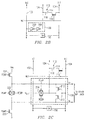
- FIGURE 2A describes one embodiment where the voltage driver circuit 130 couples the bit line BLT 104 to the cell plate line 124 of the associated memory cell.
- the voltage driver circuit 130 includes at least one inverter 200 with a predetermined delay.
- the inverter 200 may constructed using one n-channel transistor and one p-channel transistor (not shown), and additional inverters may be utilized. It will be understood that in this embodiment, the other columns of memory cells will be configured in a similar fashion.
- FIGURE 2B describes one embodiment where the voltage driver circuit 130 couples the complement bit line BLC 104 to the cell plate line 124 of the associated memory cell
- the voltage driver circuit 130 includes a buffer circuit with a predetermined delay, and preferably includes two inverters 202 and 204.
- the inverters 202, 204 may constructed using one n-channel transistor and one p-channel transistor (not shown), and additional inverters may be utilized. It will be understood that in this embodiment, the other columns of memory cells will be configured in a similar fashion.
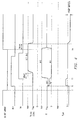
- FIGURE 2C preferably describes another embodiment where the voltage driver circuit 130 couples the bit line BLT 104 to the cell plate line 124 of the associated memory cell.
- This embodiment is similar to the embodiment shown in FIGURE 2A with additional circuitry which helps reduce power dissipation.
- the voltage driver circuit 130 includes an n-channel transistor 210 and a p-channel transistor 212 configured as an inverter, with the input connected to BLT104 and the output connected to the cell plate line 124.
- a S/D of transistor 210 is connected to a line VL and a S/D of transistor 212 is connected to a line VH.
- the line VH and VL provide a mechanism to turn-off operation of the inverter (210, 212). When the voltage on VH and VL are approximately equal, no current flows through transistors 210, 212 and the inverter is inoperative.
- the voltage levels on the lines VH and VL are set by operation of an n-channel transistor 220, a transmission gate 222, and a p-channel transistor 224, as shown.
- a signal PUMP provides a control signal for determining the voltage on the lines VH and VL, and further provides control of another transmission gate 214 (part of reference circuit 130 coupling/decoupling the reference voltage Vblp to the cell plate line 124. In operation when the PUMP signal is active, VH is high and VL is low, thereby providing power to the inverter (210, 212) and decoupling Vblp from the cell plate line 124.
- the complement bit line BLC 102 may be utilized instead of the true bit line BLT 104 with the addition of another inverter (210,212).
- the transmission gates 214, 222 may alternatively be single transistor gates (controlled by PUMP or the PUMP complement).
- the PUMP signal can be generated using a delayed version of the sense amplifier enable signal SA or generated from other clocking signals present in the memory array.
- the PUMP signal is activated after the signal SA is activated and deactivated after the word line is deactivated.
- the PUMP signal may be deactivated after the SHORT ARRAY signal is activated (high), but this may cause additional power dissipation.
- One embodiment utilizes a delayed version of the signal SA
- An alternative embodiment utilizes the activation of the SHORT ARRAY signal to trigger the deactivation of the PUMP signal, or the deactivation/activation of some other timing signal to deactivate the PUMP signal at a time that is closely proximate the activation of the SHORT ARRAY signal.
- This provides the result that the voltage on the cell plate line 124 (i.e., the second plate 116 of the capacitor element 112) is substantially the same voltage (at substantially the same time) as an intermediate voltage (Vblp on Vdd/2) when the intermediate voltage level is present on the bit line BLT.
- the general operation of the present invention is as follows:
- the bit line is equilibrated and pre-charged to an intermediate voltage.
- the word line is activated producing a small voltage differential across the true bit line and complement bit line (depending on the value stored in the active memory cell).
- the sense amplifier is enabled detecting the differential and generating a high logic voltage and on the true bit line and a low logic voltage on the complement bit line, or vice versa, depending on the value stored in the active memory cell (read/refresh operation).
- the voltage values generated on the two bit lines will also depend on the logic value if the memory cell is being overwritten (write operation).
- the complement logic voltage level (or substantially complement level) is applied to the cell plate line connected to the active memory cell.
- the word line is then deactivated storing the voltage present on the bit line to the capacitor (or charge-storing device) of the memory cell.
- an intermediate voltage is applied to the cell plate line connected to the previously active memory cell.
- Application of the intermediate voltage provides a "pumping" effect to the voltage stored on the memory cell, thereby raising/lowering the voltage of the stored value to a higher/lower voltage level (storing high/low). Operation of the present invention results in an increased bit line voltage differential during the subsequent read of the memory cell.
- the intermediate voltage is a predetermined voltage level in the range between the logic high voltage level and the logic low voltage level.
- the intermediate voltage is substantially equal to Vblp (or Vdd/2).
- FIGURES 3 and 4 there are shown detailed timing diagrams illustrating a read operation for a logic one and a logic zero, respectively, stored in the memory cell for the embodiments shown in FIGURES 2A and 2B.
- the read operation (reading a logic one stored in the memory cell) shown in FIGURE 3 generally begins at a time T1 when the SHORT ARRAY signal is deactivated (low) resulting in the precharge and equilibration of the bit lines (BLT, BLC) to a voltage Vblp (intermediate voltage).
- Vblp intermediate voltage
- the Vblp voltage is also applied to the cell plate line 124 of the active memory cell (shown as Vplate).
- the word line WL1 is activated turning on the access transistor 110 and coupling the capacitor (or charge-storing device) 112 to the bit line BLT 104.
- a dummy cell (not shown) is also activated coupling a voltage reference Vref (not shown, and preferably about Vdd/3) to the bit line BLC 102.
- Vref voltage reference
- a differential voltage is generated on the bit lines BLC 102 and BLT 104.
- the SA signal is activated.
- the activated sense amplifier 150 amplifies the differential voltage present on the bit lines BLC 102 and BLT 104 generating a logic high voltage on the BLT 104 and a logic low voltage on the BLC 102.
- the reference voltage circuits 130 in the embodiments shown in FIGURES 2A and 2B couple the bit line BLT 104 (inverted) or the bit line BLC 102, respectively, to the cell plate line 124 (Vplate), the voltage applied to the cell plate line 124 (Vplate) is a logic low voltage.
- a predetermined delay associated with the voltage driver circuits 130 is generated, as shown in FIGURE 3.
- the predetermined delay is sufficient to allow the sense amplifier 150 to sense the bit lines and generate a logic high and logic low on the bit lines before the cell plate line 124 goes low (i.e., before the voltage driver circuit 130 activates). This should help reduce any potential noise during sense that may be caused by the switching of voltage driver circuit 130.
- the SHORT ARRAY signal is activated (high) for the next read/write operation, which precharges and equilibrates the bit lines BLC 102 and BLT 104 to voltage Vblp.
- the voltage driver circuit 130 receives this input voltage and applies the voltage Vblp (intermediate voltage) to the cell plate line 124 (after the predetermined delay).
- Vblp intermediate voltage
- increasing the voltage of the cell plate line from logic low to the intermediate voltage (after the memory cell is written logic high) provides a "pumping" mechanism that increases, or pumps, the voltage in the memory cell (see Figure 3, identified as Vcell) to a value greater than the logic high voltage.
- the amount of increased voltage is referred to as pump margin. It will be understood that the pumped voltage stored in the memory provides an increase in the voltage differential on the bit lines during a subsequent read operation of the memory cell.
- a read operation (reading a logic zero stored in the memory cell) shown in FIGURE 4 generally begins at a time T1 when the SHORT ARRAY signal is deactivated (low) resulting in the precharge and equilibration of the bit lines (BLT, BLC) to a voltage Vblp (intermediate voltage).
- Vblp intermediate voltage
- the Vblp voltage is also applied to the cell plate line 124 of the active memory cell (shown as Vplate).
- the word line WL1 is activated turning on the access transistor 110 and coupling the capacitor (or charge storing device) 112 to the bit line BLT 104.
- a dummy cell (not shown) is also activated coupling a voltage reference Vref (not shown, and preferably about Vdd/3) to the bit line BLC 102.
- Vref voltage reference
- a differential voltage is generated on the bit lines BLC 102 and BLT 104.
- the SA signal is activated.
- the activated sense amplifier 150 amplifies the differential voltage present on the bit lines BLC 102 and BLT 104 generating a logic low voltage on the BLT 104 and a logic high voltage on the BLC 102.
- the reference voltage circuits 130 in the embodiments shown in FIGURES 2A and 2B couple the bit line BLT 104 (inverted) or the bit line BLC 102, respectively, to the cell plate line 124 (Vplate) the voltage applied to the cell plate line 124 (Vplate) is a logic high voltage.
- the SHORT ARRAY signal is activated (high) for the next read/write operation, which precharges and equilibrates the bit lines BLC 102 and BLT 104 to voltage Vblp.
- the voltage driver circuit 130 receives this input voltage and applies the voltage Vblp (intermediate voltage) to the cell plate line 124 (after the predetermined delay).
- decreasing the voltage of the cell plate line from logic high to the intermediate voltage provides a "pumping" mechanism that decreases, or pumps, the voltage in the memory cell (see Figure 3, identified as Vcell) to a value less than the logic low voltage.
- the amount of decreased voltage is referred to as pump margin. It will be understood that the pumped (down) voltage stored in the memory provides a increase in the voltage differential on the bit lines during a subsequent read operation of the memory cell.
- FIGURES 5 and 6 there are shown detailed timing diagrams illustrating a read operation for a logic one and a logic zero, respectively, stored in the memory cell for the embodiment shown in FIGURE 2C.
- the read operation (reading a logic one stored in the memory cell) shown in FIGURE 5 is similar to the read operation in FIGURE 3 until after the activation of the sense amplifier 150 at time T3. After a predetermined delay (sufficient to allow the sense amplifier 150 to sense the bit lines and generate a logic high and logic low on the bit lines). a PUMP signal is activated which applies a logic low to the cell plate line 124. Because the voltage driver circuit 130 in the embodiment shown in FIGURE 2C couples the bit line BLT 104 (inverted) to the cell plate line 124 (Vplate), the voltage applied to the cell plate line 124 (Vplate) is a logic low voltage. It will be understood another alternative embodiment (not shown) would include an additional inverter configured in series with the inverter (210,212) with the input coupled to the complement bit line BLC 104 instead of the true bit line BLT 102.
- the PUMP signal is deactivated resulting in application of the voltage Vblp (the intermediate voltage) to the cell plate line 124.
- Vblp the intermediate voltage
- Increasing the voltage of the cell plate line 124 from logic low to the intermediate voltage provides the pumping mechanism that increases, or pumps, the voltage in the memory cell (see Figure 5, identified as Vcell) to a value greater than the logic high voltage, providing the pump margin.
- the pumped voltage stored in the memory provides an increase in the voltage differential on the bit lines during a subsequent read operation of the memory cell.
- the additional circuitry shown in FIGURE 2C helps reduce power dissipation that would occur with the inverter (210, 212) activated when its input is the voltage Vblp (the intermediate voltage).
- a read operation (reading a logic zero stored in the memory cell) shown in FIGURE 6 is similar to the read operation in FIGURE 5.
- the PUMP signal is activated which applies a logic high to the cell plate line 124.
- the voltage driver circuit 130 in the embodiment shown in FIGURE 2C couples the bit line BLT 104 (inverted) to the cell plate line 124 (Vplate), the voltage applied to the cell plate line 124 (Vplate) is a logic high voltage.
- the PUMP signal is deactivated resulting in application of the voltage Vblp (the intermediate voltage) to the cell plate line 124.
- Vblp the intermediate voltage
- Decreasing the voltage of the cell plate line 124 from logic high to the intermediate voltage provides the pumping mechanism that decreases, or pumps, the voltage in the memory cell (see Figure 5, identified as Vcell) to a value less than the logic low voltage, providing the pump margin.
- the pumped voltage stored in the memory provides an increase in the voltage differential on the bit lines during a subsequent read operation of the memory cell.
- the present invention provides a circuit and method of increasing the stored voltage (greater than a logic one voltage level) in a memory cell by holding the memory cell plate 116 at a logic low during the writing of a logic one to the memory cell. and then raising the voltage at the memory cell plate 116 to an intermediate voltage after the word line is deactivated. Similarly, it decreases the stored voltage (less than a logic zero voltage level) in a memory cell by holding the memory cell plate 116 at a logic high during the writing of a logic zero to the memory cell, and then decreasing the voltage at the memory cell plate 116 to an intermediate voltage after the word line is deactivated. This results in increased differential voltages on the bit lines during a read operation of the memory cell.
Landscapes
- Engineering & Computer Science (AREA)
- Microelectronics & Electronic Packaging (AREA)
- Computer Hardware Design (AREA)
- Dram (AREA)
- Static Random-Access Memory (AREA)
Abstract
Description
Claims (23)
Applications Claiming Priority (2)
| Application Number | Priority Date | Filing Date | Title |
|---|---|---|---|
| US751367 | 2000-12-29 | ||
| US09/751,367 US6469941B2 (en) | 2000-12-29 | 2000-12-29 | Apparatus and method for pumping memory cells in a memory |
Publications (2)
| Publication Number | Publication Date |
|---|---|
| EP1220227A2 true EP1220227A2 (en) | 2002-07-03 |
| EP1220227A3 EP1220227A3 (en) | 2004-02-04 |
Family
ID=25021672
Family Applications (1)
| Application Number | Title | Priority Date | Filing Date |
|---|---|---|---|
| EP01310105A Withdrawn EP1220227A3 (en) | 2000-12-29 | 2001-12-03 | Apparatus and method for pumping memory cells in a memory. |
Country Status (3)
| Country | Link |
|---|---|
| US (1) | US6469941B2 (en) |
| EP (1) | EP1220227A3 (en) |
| JP (1) | JP2002208273A (en) |
Families Citing this family (5)
| Publication number | Priority date | Publication date | Assignee | Title |
|---|---|---|---|---|
| JP2005174426A (en) * | 2003-12-09 | 2005-06-30 | Micron Technology Inc | Deactivation of selectable memory word lines |
| CN100449648C (en) * | 2003-12-24 | 2009-01-07 | 上海贝岭股份有限公司 | Charge pump circuit driven by low operating voltage |
| DE102005003461A1 (en) * | 2005-01-25 | 2006-08-03 | Infineon Technologies Ag | Integrated semiconductor memory e.g. dynamic RAM, for storing digital information, has selection transistor, where capacitor electrode connected to complementary secondary bit line and is not connected to transistor |
| KR20100118839A (en) * | 2009-04-29 | 2010-11-08 | 삼성전자주식회사 | Semiconductor memory device |
| US9105351B2 (en) * | 2011-11-09 | 2015-08-11 | Semiconductor Energy Laboratory Co., Ltd. | Semiconductor memory device including amplifier circuit |
Family Cites Families (13)
| Publication number | Priority date | Publication date | Assignee | Title |
|---|---|---|---|---|
| US4769784A (en) * | 1986-08-19 | 1988-09-06 | Advanced Micro Devices, Inc. | Capacitor-plate bias generator for CMOS DRAM memories |
| GB9007793D0 (en) * | 1990-04-06 | 1990-06-06 | Foss Richard C | Dram cell plate and precharge voltage generator |
| JP3179793B2 (en) * | 1990-05-30 | 2001-06-25 | 三菱電機株式会社 | Semiconductor memory device and reading method therefor |
| JP3116431B2 (en) * | 1991-06-27 | 2000-12-11 | 日本電気株式会社 | Semiconductor storage device |
| JPH05182458A (en) * | 1991-12-26 | 1993-07-23 | Toshiba Corp | Semiconductor memory |
| JPH05242672A (en) * | 1992-02-04 | 1993-09-21 | Nec Corp | Semiconductor dynamic memory |
| JPH05250875A (en) * | 1992-02-27 | 1993-09-28 | Nec Corp | Semiconductor storage device |
| US5414656A (en) | 1994-03-23 | 1995-05-09 | Kenney; Donald M. | Low charge consumption memory |
| US5508962A (en) * | 1994-06-29 | 1996-04-16 | Texas Instruments Incorporated | Apparatus and method for an active field plate bias generator |
| JP3270294B2 (en) * | 1995-01-05 | 2002-04-02 | 株式会社東芝 | Semiconductor storage device |
| US5734603A (en) * | 1997-02-10 | 1998-03-31 | Powerchip Semiconductor Corp. | Method and circuit for reducing cell plate noise |
| KR100281280B1 (en) * | 1997-06-30 | 2001-03-02 | 김영환 | Cell Plate Voltage Generator of Semiconductor Memory Devices |
| US6236598B1 (en) * | 1999-08-11 | 2001-05-22 | Taiwan Semiconductor Manufacturing Company | Clamping circuit for cell plate in DRAM |
-
2000
- 2000-12-29 US US09/751,367 patent/US6469941B2/en not_active Expired - Lifetime
-
2001
- 2001-12-03 EP EP01310105A patent/EP1220227A3/en not_active Withdrawn
- 2001-12-28 JP JP2001400099A patent/JP2002208273A/en active Pending
Also Published As
| Publication number | Publication date |
|---|---|
| JP2002208273A (en) | 2002-07-26 |
| EP1220227A3 (en) | 2004-02-04 |
| US20020085408A1 (en) | 2002-07-04 |
| US6469941B2 (en) | 2002-10-22 |
Similar Documents
| Publication | Publication Date | Title |
|---|---|---|
| US7626877B2 (en) | Low voltage sense amplifier and sensing method | |
| US6754121B2 (en) | Sense amplifying circuit and method | |
| US6046951A (en) | Process for controlling the read circuit of a memory plane and corresponding memory device | |
| US5220527A (en) | Dynamic type semiconductor memory device | |
| US5255235A (en) | Dynamic random access memory with dummy word lines connected to bit line potential adjusting capacitors | |
| US7613024B2 (en) | Local digit line architecture and method for memory devices having multi-bit or low capacitance memory cells | |
| US6400629B1 (en) | System and method for early write to memory by holding bitline at fixed potential | |
| US7450455B2 (en) | Semiconductor memory device and driving method thereof | |
| JPS61142591A (en) | Semiconductor storage device | |
| US5323345A (en) | Semiconductor memory device having read/write circuitry | |
| US8027193B2 (en) | Semiconductor memory device having bit line disturbance preventing unit | |
| KR100368705B1 (en) | Variable voltage isolation gate | |
| JP2002050181A (en) | Semiconductor storage device | |
| US5666306A (en) | Multiplication of storage capacitance in memory cells by using the Miller effect | |
| KR100244862B1 (en) | Semiconductor memory device having dummy word lines and method for controlling the same | |
| US6570799B1 (en) | Precharge and reference voltage technique for dynamic random access memories | |
| US6198681B1 (en) | Sense amplifier for low voltage memory arrays | |
| US6469941B2 (en) | Apparatus and method for pumping memory cells in a memory | |
| US6236598B1 (en) | Clamping circuit for cell plate in DRAM | |
| US7336522B2 (en) | Apparatus and method to reduce undesirable effects caused by a fault in a memory device | |
| US7149138B2 (en) | Increasing a refresh period in a semiconductor memory device | |
| US6542399B2 (en) | Apparatus and method for pumping memory cells in a memory | |
| US5995410A (en) | Multiplication of storage capacitance in memory cells by using the Miller effect | |
| US5870338A (en) | Circuit and method for reading and writing data in a memory device | |
| US20260080935A1 (en) | Memory device |
Legal Events
| Date | Code | Title | Description |
|---|---|---|---|
| PUAI | Public reference made under article 153(3) epc to a published international application that has entered the european phase |
Free format text: ORIGINAL CODE: 0009012 |
|
| AK | Designated contracting states |
Kind code of ref document: A2 Designated state(s): AT BE CH CY DE DK ES FI FR GB GR IE IT LI LU MC NL PT SE TR |
|
| AX | Request for extension of the european patent |
Free format text: AL;LT;LV;MK;RO;SI |
|
| PUAL | Search report despatched |
Free format text: ORIGINAL CODE: 0009013 |
|
| AK | Designated contracting states |
Kind code of ref document: A3 Designated state(s): AT BE CH CY DE DK ES FI FR GB GR IE IT LI LU MC NL PT SE TR |
|
| AX | Request for extension of the european patent |
Extension state: AL LT LV MK RO SI |
|
| 17P | Request for examination filed |
Effective date: 20040729 |
|
| AKX | Designation fees paid |
Designated state(s): DE FR GB IT |
|
| 17Q | First examination report despatched |
Effective date: 20050601 |
|
| STAA | Information on the status of an ep patent application or granted ep patent |
Free format text: STATUS: THE APPLICATION IS DEEMED TO BE WITHDRAWN |
|
| 18D | Application deemed to be withdrawn |
Effective date: 20061228 |