EP1220193A2 - Brightness offset error reduction system and method for a display device - Google Patents
Brightness offset error reduction system and method for a display device Download PDFInfo
- Publication number
- EP1220193A2 EP1220193A2 EP01129974A EP01129974A EP1220193A2 EP 1220193 A2 EP1220193 A2 EP 1220193A2 EP 01129974 A EP01129974 A EP 01129974A EP 01129974 A EP01129974 A EP 01129974A EP 1220193 A2 EP1220193 A2 EP 1220193A2
- Authority
- EP
- European Patent Office
- Prior art keywords
- display device
- output voltage
- circuitry
- voltage
- brightness
- Prior art date
- Legal status (The legal status is an assumption and is not a legal conclusion. Google has not performed a legal analysis and makes no representation as to the accuracy of the status listed.)
- Granted
Links
Images


Classifications
-
- G—PHYSICS
- G09—EDUCATION; CRYPTOGRAPHY; DISPLAY; ADVERTISING; SEALS
- G09G—ARRANGEMENTS OR CIRCUITS FOR CONTROL OF INDICATING DEVICES USING STATIC MEANS TO PRESENT VARIABLE INFORMATION
- G09G3/00—Control arrangements or circuits, of interest only in connection with visual indicators other than cathode-ray tubes
- G09G3/20—Control arrangements or circuits, of interest only in connection with visual indicators other than cathode-ray tubes for presentation of an assembly of a number of characters, e.g. a page, by composing the assembly by combination of individual elements arranged in a matrix no fixed position being assigned to or needed to be assigned to the individual characters or partial characters
- G09G3/34—Control arrangements or circuits, of interest only in connection with visual indicators other than cathode-ray tubes for presentation of an assembly of a number of characters, e.g. a page, by composing the assembly by combination of individual elements arranged in a matrix no fixed position being assigned to or needed to be assigned to the individual characters or partial characters by control of light from an independent source
- G09G3/36—Control arrangements or circuits, of interest only in connection with visual indicators other than cathode-ray tubes for presentation of an assembly of a number of characters, e.g. a page, by composing the assembly by combination of individual elements arranged in a matrix no fixed position being assigned to or needed to be assigned to the individual characters or partial characters by control of light from an independent source using liquid crystals
- G09G3/3611—Control of matrices with row and column drivers
-
- G—PHYSICS
- G09—EDUCATION; CRYPTOGRAPHY; DISPLAY; ADVERTISING; SEALS
- G09G—ARRANGEMENTS OR CIRCUITS FOR CONTROL OF INDICATING DEVICES USING STATIC MEANS TO PRESENT VARIABLE INFORMATION
- G09G3/00—Control arrangements or circuits, of interest only in connection with visual indicators other than cathode-ray tubes
- G09G3/20—Control arrangements or circuits, of interest only in connection with visual indicators other than cathode-ray tubes for presentation of an assembly of a number of characters, e.g. a page, by composing the assembly by combination of individual elements arranged in a matrix no fixed position being assigned to or needed to be assigned to the individual characters or partial characters
- G09G3/34—Control arrangements or circuits, of interest only in connection with visual indicators other than cathode-ray tubes for presentation of an assembly of a number of characters, e.g. a page, by composing the assembly by combination of individual elements arranged in a matrix no fixed position being assigned to or needed to be assigned to the individual characters or partial characters by control of light from an independent source
- G09G3/3406—Control of illumination source
-
- G—PHYSICS
- G09—EDUCATION; CRYPTOGRAPHY; DISPLAY; ADVERTISING; SEALS
- G09G—ARRANGEMENTS OR CIRCUITS FOR CONTROL OF INDICATING DEVICES USING STATIC MEANS TO PRESENT VARIABLE INFORMATION
- G09G5/00—Control arrangements or circuits for visual indicators common to cathode-ray tube indicators and other visual indicators
- G09G5/10—Intensity circuits
-
- G—PHYSICS
- G09—EDUCATION; CRYPTOGRAPHY; DISPLAY; ADVERTISING; SEALS
- G09G—ARRANGEMENTS OR CIRCUITS FOR CONTROL OF INDICATING DEVICES USING STATIC MEANS TO PRESENT VARIABLE INFORMATION
- G09G2320/00—Control of display operating conditions
- G09G2320/06—Adjustment of display parameters
- G09G2320/0606—Manual adjustment
-
- G—PHYSICS
- G09—EDUCATION; CRYPTOGRAPHY; DISPLAY; ADVERTISING; SEALS
- G09G—ARRANGEMENTS OR CIRCUITS FOR CONTROL OF INDICATING DEVICES USING STATIC MEANS TO PRESENT VARIABLE INFORMATION
- G09G2320/00—Control of display operating conditions
- G09G2320/06—Adjustment of display parameters
- G09G2320/0626—Adjustment of display parameters for control of overall brightness
-
- G—PHYSICS
- G09—EDUCATION; CRYPTOGRAPHY; DISPLAY; ADVERTISING; SEALS
- G09G—ARRANGEMENTS OR CIRCUITS FOR CONTROL OF INDICATING DEVICES USING STATIC MEANS TO PRESENT VARIABLE INFORMATION
- G09G2360/00—Aspects of the architecture of display systems
- G09G2360/14—Detecting light within display terminals, e.g. using a single or a plurality of photosensors
- G09G2360/144—Detecting light within display terminals, e.g. using a single or a plurality of photosensors the light being ambient light
Definitions
- This invention generally relates to display devices. More particularly, this invention relates to display devices having offset error reduction for brightness resolution control.
- Display devices are used in a variety of consumer and industrial products to display data, charts, graphs, messages, other images, information, and the like.
- Backlight display devices which may be backlit or frontlit, have a backlight positioned to provide light for a display panel.
- Emissive display devices have pixels that are the emissive light source.
- the pixel light source may be CRT phosphor, FED phosphor, a light emitting diode (LED), an organic diode, an electroluminescent, or any emissive display technology.
- the backlight may be a fluorescent tube, an electro-luminescent device, LED, a gaseous discharge lamp, a plasma panel, and the like.
- the display panel may be a passive or active matrix liquid crystal display (LCD).
- LCD liquid crystal display
- the backlight and display panel are connected to control circuitry, which is connected to a voltage supply.
- the display device may be separate or incorporated with other components, such as a dashboard in an automobile or other vehicle, a portable electronic device, and the like.
- a display device controls brightness in relation to the environment of the display device and user preferences.
- the brightness may remain at an essentially fixed level for an extended time period.
- the brightness is adjusted frequently because of changes in the environment, user preferences, and similar factors.
- the control circuitry may automatically adjust the brightness.
- a user may further adjust or manually set the brightness through a user interface, such as a knob, switch, keypad, touch screen, remote device, or the like.
- the control circuitry receives an input signal indicating a user preference, an environmental condition, or the like.
- the control circuitry selects a luminance value corresponding to the input signal.
- the luminance value is converted into an analog control signal or an output voltage.
- the control circuitry provides the analog control signal to the backlight, the display panel, or both.
- the control circuitry may modify or further adjust the analog control signal and may combine the analog control signal with other inputs to operate the display device at the desired brightness.
- the control circuitry typically has a single digital-to-analog converter (DAC) or PWM plus a filter to convert the luminance into the analog control signal.
- DAC digital-to-analog converter
- a higher resolution DAC may be used to provide sufficient adjustment resolution for lower levels, the dynamic range, and an exponential output signal.
- a typical DAC for brightness resolution control may have 12 bits for use in a dynamic range of about 0.5 nits through about 400 nits.
- the DAC may introduce offset errors into the analog control signal or output voltage. Offset errors are inherent to DACs and may result from the digitizing process and other factors. Offset errors generally are constant errors over essentially an entire dynamic range. Other DAC errors such as quantization errors and linearity errors may result. For digital processing, signal values may be rounded or truncated to form an integer. A quantization error may result when the responsive analog control signal provides a brightness level different from the brightness level corresponding to the selected luminance value. As brightness resolution increases, more quantization errors may result due to the increase in brightness adjustment steps and other factors. Additionally, as the brightness level decreases, the offset error and quantization error increases the error of the desired output brightness.
- the analog control signal from the DAC has constant ratio steps or an exponential progression for a user to perceive the brightness adjustments.
- Brightness adjustments need constant ratio steps which results in the need for variable resolution control because of how a human eye perceives changes in brightness.
- the human vision system perceives changes in brightness non-linearly and logarithmically. A user perceives a brightness change from about 10 nits to about 12 nits as essentially equal to a brightness change from about 100 nits to about 120 nits. As the brightness level decreases, more brightness control resolution is needed to accurately provide the brightness step changes that are perceived as uniform by a user.
- a brightness offset and quantization error of 1 nit is about one percent of a brightness level equal to 100 nits.
- the same brightness error is about 10 percent of a brightness level equal to 10 nits.
- Offset errors generally are unacceptable, especially at lower luminance values.
- a higher resolution DAC may reduce the offset errors, but increase the cost of the display device.
- a higher resolution DAC may reduce the quantization errors, but increase the cost of the display device and generally does not significantly reduce the offset error because virtually all DACs have offset error.
- Other approaches include correcting the offset error on a per unit basis or using a complex feedback system that requires a precise digital-to-analog converter with corresponding software to provide the offset error correction. These approaches are difficult to implement and may increase the cost of the display device.
- the brightness offset error reduction system may divide the output voltage from digital-to-analog (DAC) circuitry used to control the brightness of the display device. This division of the output voltage may be used to reduce brightness offset errors and may be used to increase the brightness resolution at low luminance levels, such as nighttime applications.
- DAC digital-to-analog
- the brightness offset error reduction system may be used in automotive and similar applications where the maximum nighttime brightness is a divided ratio of the maximum daytime brightness.
- a display device with a brightness offset error reduction system has a lighted display, digital-to-analog (DAC) circuitry, and voltage divider circuitry.
- the voltage divider circuitry is operatively connected to receive an output voltage from digital-to-analog converter (DAC) circuitry.
- DAC digital-to-analog converter
- the voltage divider circuitry provides a fractional portion of the output voltage as a divided output voltage to the lighted display.
- a brightness offset error reduction system for a display device has digital-to-analog converter (DAC) circuitry and voltage divider circuitry.
- the voltage divider circuitry has a switching mechanism and is operatively connected to receive an output voltage from the DAC circuitry.
- the voltage divider circuitry provides a divided output voltage when the switching mechanism is engaged.
- a luminance value is converted into an output voltage.
- a determination is made whether the output voltage is to be divided.
- a fractional portion of the output voltage is provided when the output voltage is to be divided.
- Figure 1 represents a side view of a backlight display device having an automatic brightness control system according to one embodiment.
- Figure 2 represents a front view of the backlight display device shown in Figure 1.
- Figure 3 represents a block diagram and flowchart of a brightness offset error reduction system for a display device according to one embodiment.
- Figure 4 shows the relationship between the percent reduction of percent ratio error and the brightness step number.
- Figure 5 shows a comparison of nighttime brightness ratios for a maximum brightness range limit of 60 nits.
- Figure 6 shows a comparison of nighttime brightness ratios for a maximum brightness range limit of 16 nits.
- Figures 1 and 2 represent block diagrams of a backlight display device 100 having a brightness offset error reduction system according to one embodiment.
- Figure 1 shows a side view of the backlight display device 100.
- Figure 2 shows a front view of the backlight display device 100.
- the backlight display device 100 has a backlight 102, a display panel 104, a bezel 106, control circuitry 108, a voltage supply 110, a user interface 112, and an ambient light sensor 114.
- the backlight display device 100 may have additional or fewer components and may have different configurations.
- the backlight display device 100 may provide a reverse image for rear projection, may project an image onto a display surface (not shown), may have one or more magnification lens (not shown) and reflective surfaces (not show), and may work with or have other components.
- the backlight display device 100 may be incorporated in a navigation radio system for an automobile or other vehicle.
- the backlight display device 100 may be built-in or integrated with a dashboard, control panel, or other part of an automobile or other vehicle.
- the backlight display device 100 also may be built-in or integrated with an electronic device such as a cell phone or other communication device, a laptop or other personal computer, a personal organizer, and the like. Additionally, the backlight display device 100 may be separate or a separable component. While configurations and modes of operation are described, other configurations and modes of operation may be used.
- the backlight 102 and the display panel 104 form a liquid crystal display (LCD).
- the backlight 102 and the display panel 104 may be a passive or active matrix LCD and may comprise another type of lighted display, which may be a backlit or frontlit display and may be an emissive display such as an LED or other pixel light source.
- the backlight 102 is operatively disposed to provide light for operation of the display panel 104.
- the backlight 102 and the display panel 104 may provide monochrome, color, or a combination of monochrome and color displays.
- the backlight 102 is a cold cathode fluorescent lamp.
- the backlight 102 may be one or more fluorescent tubes, electro-luminescent devices, gaseous discharge lamps, plasma panels, LED, a combination, and the like, which may be aligned.
- the backlight 102 may include multiple or sub backlights.
- the display panel 104 may be selected based on the type of backlight and may have multiple or sub display panels.
- the bezel 106 may extend around and hold the outer perimeter of the display panel 104.
- the bezel 106 may have various configurations and may extend around part or only a portion of the outer perimeter.
- the bezel 106 may hold or extend around other components such as the backlight 102.
- the bezel 106 also may include additional bezels and may be connected with or be part of another component such as a dashboard in an automobile.
- the control circuitry 108 provides an image signal to the backlight 102 and/or the display panel 104.
- the control circuitry 108 may include one or more microprocessors (not shown) and may be part or incorporated with other circuitry such as a central processing unit or a vehicle control unit.
- the control circuitry 108 may be completely or partially provided on one or more integrated circuit (IC) chips.
- the control circuitry 108 may have other circuitry for control and operation of the backlight display device 100 such as a transceiver, one or more memory devices, and the like.
- the control circuitry 108 also is connected to a voltage supply 110, which may be provided by an automotive battery or electrical system, another type of battery, a household current supply, or other suitable power source.
- the control circuitry 108 may generate the image signal and may pass the image signal from another source (not shown).
- the image signal may be based upon one or more radio signals, one or more signals from a global positioning system (GPS), data stored in a memory device, user inputted data, a combination or combinations of these signals and data, and the like.
- GPS global positioning system
- the control circuitry 108 provides a command brightness signal or output voltage to control the brightness of the display panel 104.
- the command brightness signal or output voltage corresponds to a luminance value for the desired or selected brightness.
- the command brightness signal changes as different luminance values are used.
- the control circuitry 108 may receive one or more input or analog signals indicating a user preference, an environmental condition, and other factors.
- the user interface 112, the ambient light sensor 114, and other input devices may provide the input signal.
- the control circuitry 108 uses one or more of the input signals to select a luminance.
- the luminance value may be in the range of about 0.5 nits through about 400 nits.
- the luminance value is in the range of about 0.5 nits through about 60 nits for nighttime applications and the like. In another aspect, the luminance value is in the range of about 80 nits through 400 nits for daytime applications and the like.
- the control circuitry 108 has digital-to-analog converter (DAC) circuitry and voltage divider circuitry (see Figure 3).
- the DAC circuitry converts the luminance value into the analog command brightness signal or an output voltage.
- the DAC circuitry may be a part or separate from the control circuitry 108.
- the voltage divider circuitry may divide the output voltage to produce a divided output voltage.
- the control circuitry 108 may have a microprocessor (not shown) or other circuitry to determine whether the output voltage is to be divided.
- the control circuitry 108 opens and closes a switching mechanism (see Figure 3) depending upon whether the output voltage is to be divided.
- the control circuitry 108 provides the divided output voltage or the undivided output voltage as the command brightness signal to the backlight 102, the display panel 104, or both.
- the backlight 102 or the control circuitry 108 may have a backlight inverter (not shown) for receiving the output voltage and providing the command brightness signal to the backlight 102.
- the control circuitry 108 may modify or further adjust the command brightness signal and may combine the command brightness signal with other inputs to operate the backlight display device 100 at the desired or selected brightness.
- the voltage divider circuitry may divide the output voltage under some operating conditions and may not divide the output voltage under other operating conditions.
- the voltage divider circuitry may divide the output voltage when lower luminance values are used, such as during nighttime conditions.
- the divided output voltage is a fractional portion of the output voltage.
- a fractional portion includes any value less than the output voltage. In one aspect, the fractional portion is in the range of about 3 percent through about 50 percent.
- the user interface 112 enables a user to interact with the backlight display device 100.
- the user interface 112 may provide one or more input digital or analog signals to the control circuitry 108.
- the input signal may indicate one or more user preferences for brightness of the backlight display device 100.
- the user interface 112 is disposed in or on the outer surface of the bezel 106.
- the user interface 112 may be one or more knobs or push buttons.
- the user interface 112 also may be other types of manual controls, a touch screen, electronic input from another device, and the like.
- the user interface 112 may be located elsewhere, may be incorporated with another controller or user interface, and may be included in a remote control device.
- the ambient light sensor 114 is connected to provide an input or analog signal to the control circuitry 108.
- the input signal may be indicative of the ambient light on the display panel 104.
- the ambient light sensor 114 may include a photodiode (not show) and may be a logarithmic sensor or another type of sensor.
- the ambient light sensor 114 may have a logarithmic amplifier (not shown), other components, and other configurations.
- the logarithmic amplifier may be part of the control circuitry 108.
- the ambient light sensor 114 or the photodiode is positioned on an outer surface of the bezel 106. The ambient light sensor 114 or the photodiode may be placed elsewhere.
- the ambient light sensor 114 may be temperature compensated and may discriminate between daytime and nighttime conditions for determination of display luminance and control functions.
- the ambient light sensor 114 may operate in a dynamic range of lighting conditions such as those encountered in an automotive environment.
- the ambient light sensor 114 may have a dynamic range of about four decades of lighting conditions. In one aspect, the ambient light sensor 114 operates on less than about five volts from a single positive power supply.
- the ambient light sensor 114 may operate on other voltage ranges and with positive and negative supplies.
- the ambient light sensor 114 senses ambient light.
- a photodiode (not shown) in the ambient light sensor 114 provides an analog signal.
- a logarithmic amplifier (not shown) amplifies the analog signal.
- the control circuitry 108 has an analog-to-digital converter (not shown) to convert the analog signal into a first input signal, which may be filtered or averaged.
- the user interface 112 may provide a second input signal.
- the control circuitry 108 uses at least one of the first and second input signals to select a brightness or luminance value.
- the digital-to-analog converter (DAC) circuitry converts the luminance value into a command brightness signal or output voltage for controlling the luminance or brightness of the backlight display device. When lower luminance values are used such as during nighttime and similar applications, the voltage divider circuitry may be used to divide the output voltage.
- FIG. 3 is a block diagram and flowchart of a brightness offset error reduction system method for a display device.
- digital-to-analog (DAC) converter circuitry 302 is operatively connected to a first amplifier circuit 304, voltage divider circuitry 306, and a second amplifier circuit 308.
- Operatively connected includes direct or indirect connections as long as the signals or voltages pass electrically or otherwise. Indirect connections may include other circuitry and adjusting or providing other signals or voltages.
- the DAC converter circuitry 302, first amplifier circuit 304, the voltage divider circuitry 306, and the second amplifier circuit 308 may be provided on one or more integrated circuit (IC) chips.
- the brightness offset reduction system may have additional or fewer components and other configurations.
- the DAC circuitry 302 may include one or more DACs.
- the DAC circuitry 302 also may have multiple DACs operatively connected in a cascade arrangement. In a cascade arrangement, the output voltage of one DAC is the input voltage of another DAC and the output voltage of the last DAC provides the commanded brightness signal. As previously discussed, the DAC circuitry 302 provides an output voltage.
- the first amplifier circuit 304 is connected to receive the output voltage from the DAC circuitry 302.
- the first amplifier circuit 304 may include a first operational amplifier 316 operatively connected from the noninverting input through a resistor 312 to the DAC circuitry 302.
- the resistor 312 is connected in parallel to a first grounded resistor 310.
- the resistor 312 also is connected in parallel to a resistor 314, connected to an offset reference voltage V OFF .
- the resistor 314 may be grounded.
- the operational amplifier 316 has a negative feedback loop including a resistor 320 in parallel with a second grounded resistor 318.
- the first amplifier circuit 304 may have other configurations and circuitry including multistage amplifiers and additional or fewer components.
- the first amplifier circuit 304 is operatively connected to provide an amplified output voltage to the voltage divider circuitry 306.
- the output voltage from the DAC circuitry 302 is amplified by times a gain factor and offset by the offset reference voltage V OFF .
- the second amplifier circuit 308 is operatively connected to receive a divider output signal from the voltage divider circuitry 306.
- the second amplifier circuit 308 may include a second operational amplifier 328 with a negative feedback loop having a resistor 332 in series with a capacitor 334.
- the feedback loop is connected in parallel with a resistor 330, which maybe connected to a photopic feedback signal offset by V OFF .
- the second amplifier circuit 308 may have other configurations and circuitry including multistage amplifiers and additional or fewer components.
- the second amplifier circuit 308 is operatively connected to provide the command brightness signal V BRITE to the backlight, the display panel, or both.
- the voltage divider circuitry 306 receives the amplified output voltage from the first amplifier circuit 304 and provides a divider output signal to the second amplifier circuit 308.
- the divider output signal may be the amplified output voltage or a divided output voltage.
- the divider circuitry 306 has a first divider resistor 322 between the first amplifier circuit 304 and the second amplifier circuit 328.
- a second divider resistor 324 is connected in parallel with the first divider resistor 322.
- the second divider resistor 324 is connected to a switch 326.
- the voltage divider circuitry 306 may have additional or fewer components and may have different configurations.
- the voltage divider circuitry is without the switch 326.
- the switch 326 or resistor 324 is grounded and/or three or more selectable amounts of division are provided.
- the switch 326 may be any switching mechanism suitable for the circuit design of the divider circuitry 306, such as a transistor or relay.
- the switching mechanism has a JFET or MOS type transistor.
- a bipolar transistor may introduce a saturation voltage offset error.
- the switch may be positioned at other locations in the voltage divider circuitry 306.
- the control circuitry opens and closes the switch 326 depending upon whether the amplified output voltage is to be divided.
- the switch 326 may be part of or operatively connected to enabling circuitry (not shown) that opens and closes the switch 326.
- the enabling circuitry may include another DAC and a transistor.
- the divider circuitry 306 passes the amplified output voltage onto the second amplifier circuit 308 as the divider output signal.
- the switch 326 is closed or engaged, the divider circuitry 306 divides the amplified output voltage and provides a divided output voltage to the second amplifier circuit 308 as the divider output signal.
- the voltage divider circuitry 306 divides the amplified output voltage by a divider ratio D.
- R 322 is about 3,240 ohms and R 324 is about 133 ohms, resulting in a divider ratio D of about 0.04.
- the divider circuitry is selected to provide a divider ratio D in the range of about 0.04 through about 0.15. Different size resistors and other circuit arrangements may be used to obtain the same or different divider ratios.
- the voltage divider circuitry 306 reduces the brightness offset errors from the DAC circuitry 302 during low luminance levels, such as luminance levels encountered in a nighttime automobile environment.
- the voltage divider circuitry may reduce constant error over essentially an entire dynamic range and may reduce other DAC errors such as quantization errors and linearity errors.
- the human system perceives changes in brightness non-linearly and logarithmically. A user perceives a brightness change from about 10 nits to about 12 nits (a ratio of about 1.2 or its inverse) as essentially equal to a brightness change from about 100 nits to about 120 nits (a ratio of about 1.2 or its inverse). As the brightness level decreases, more brightness control resolution provides the brightness step changes perceived as uniform by a user. In addition, the acceptable amount of brightness offset error decreases as the luminance or brightness level decreases.
- a brightness offset error may introduce an offset brightness, which is the difference in brightness between the selected brightness or luminance value provided to the DAC circuitry 302 and the brightness produced by the output voltage from the DAC circuitry 302.
- B OS is essentially the same for both brightness steps B N and B N+1 . Equation 2 may be solved for the percent ratio error %RE as follows:
- the percent ratio error %RE increases as the minimum night brightness level B N decreases.
- the percent ratio error %RE also increases as brightness ratio R is increased.
- the voltage divider circuit 306 may be used to divide the output voltage from the DAC circuitry 302.
- the switch 326 may be closed during low luminance levels, such as nighttime levels and the like.
- the switch 326 also may be closed during all or part of the luminance levels associated with nighttime applications.
- the switch 326 also may be closed during other luminance levels.
- the low luminance levels are less than about 100 nits.
- the low luminance levels have a range of about 0.5 nits through about 60 nits.
- the low luminance levels may have a range between about 0.5 nits through about 30 nits.
- the brightness offset error of the DAC circuitry 302 is attenuated by the divider ratio D.
- the luminance value or data value provided to the DAC circuitry 302 is adjusted by the divider ratio D.
- the luminance value is increased by the inverse of the divider ratio (1/D).
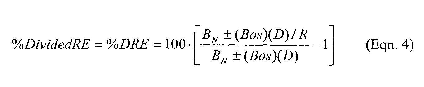
- the percent ratio error %RE may be calculated as follows:
- Figure 4 is a chart showing the relationship between the percent reduction of percent ratio error (%Reduction of %RE) and the brightness step number N according to Equation 6.
- the %Reduction of %RE is plotted for nighttime brightness maximums of 16 nits and 60 nits, which may represent the range limits for nighttime brightness.
- the voltage divider circuitry 306 may provide an improvement in the ratio error from about 40% through about 95% depending on the brightness level, the brightness step number, and the nighttime maximum brightness.
- the maximum specified value for offset brightness B OS may very and depends on the DAC. In automotive and similar applications, an offset brightness B OS of about 3.63 nits maybe the maximum specified value for a cost effective DAC. In one aspect, the voltage divider circuitry 306 essentially divides the 3.63 nits by the ratio of night to day maximum brightness values to provide the brightness ratio error reduction.
- Figure 5 shows a comparison of nighttime brightness ratios for a maximum brightness range limit of 60 nits.
- Figure 6 shows a comparison of nighttime brightness ratios for a maximum brightness range limit of 16 nits.
- These figures compare the brightness ratios from the divided output voltage to the brightness ratios from the "not divided" output signal or the amplified output signal. The desired brightness ratios are shown for comparison.
- the voltage divider improves performance more at lower luminance values (smaller brightness step numbers).
- the divider ratio D decreases the DAC offset error. The ratio error may be reduced significantly to provide suitable performance.
- the divider ratio D may be used only for part of or the lower nighttime steps.
- the switch 326 may be opened or disengaged to provide higher nighttime brightness.
- the maximum divided brightness may be about 30 nits in a nighttime brightness range of about 0.5 nits through about 60 nits. In one aspect, the maximum divided brightness is selected to avoid a noticeable brightness ratio jump when the switch is disengaged.
- an offset reference voltage V OFF allows the operational amplifiers 316, 328, and 336 to be operated with single-ended voltage supplies such as those encountered in automotive applications. Single-ended supplies essentially eliminate the need for additional power supply circuitry (not shown) for negative supply voltages (not shown).
- the voltage divider circuitry 306 operates with respect to V OFF regardless of whether the switch 326 is open or closed.
- the output of a third operational amplifier 336 is connected to the second operational amplifier 328.
- the third operational amplifier 336 may be configured to have V OFF added to a feedback signal.
- V OFF is added to a backlight luminance signal.
- the second operational amplifier 328 compares the backlight luminance feedback signal to the output signal from the voltage divider circuitry 306, thereby canceling V OFF .
- V OFF is selected to be greater than the lower operational limits of the operational amplifiers 316 and 328 when the negative supply for the amplifiers is connected to ground (single ended).
- the offset reference voltage V OFF may be any voltage suitable for operating the voltage divider circuitry and the display device. In one aspect, the offset reference voltage V OFF is less than about 1.5 volts. In another aspect, the offset reference voltage V OFF is in the range of about 0.5 volts through about 1.5 volts.
- the transfer equation for the amplified output voltage may be calculated as follows: where V OFF is the offset reference voltage, Vo 302 is the output voltage provided by the DAC circuitry 302, Vo 316 is the amplified output voltage provided by the first operational amplifier 316, V 328+ is the noninverting input signal or the divider output signal provided to second operational amplifier 328, R 312 is the resistance provided by the resistor 312, R 314 is the resistance provided by the resistor 314, R 318 is the resistance provided by the resistor 318, and R 320 is the resistance provided by the resistor 320.
- the divider output signal from the voltage divider circuitry 306 is essentially the amplified output signal and may be calculated as a gain factor times the output voltage from the DAC circuitry 302 and offset by the offset reference voltage V OFF .
- the divider output signal or the transfer function from the voltage divider circuitry 306 may be calculated as follows:
- Equation 8 Substituting in Equation 8 for Vo 316 yields the following equation:
- the voltage divider circuitry 306 divides the amplified or gained output voltage from the DAC circuitry 302 and offsets by V OFF .
- the offset error reduction system may be provided in an automotive, handheld electronics, lap tops, display screens or other single supply environment.
- the offset error reduction system may be applied to virtually any brightness control system to reduce offset errors.
- the offset error reduction system may be used when lower luminance levels (such as the maximum nighttime brightness) are a divided ratio of higher luminance levels (such as the maximum daytime brightness) or for any other luminance levels.
Landscapes
- Engineering & Computer Science (AREA)
- Physics & Mathematics (AREA)
- Computer Hardware Design (AREA)
- General Physics & Mathematics (AREA)
- Theoretical Computer Science (AREA)
- Chemical & Material Sciences (AREA)
- Crystallography & Structural Chemistry (AREA)
- Control Of Indicators Other Than Cathode Ray Tubes (AREA)
- Liquid Crystal (AREA)
- Liquid Crystal Display Device Control (AREA)
Abstract
Description





Claims (57)
- A display device having a brightness offset error reduction system, comprising:where the voltage divider circuitry provides a fractional portion of the output voltage as a divided output voltage to the lighted display.a lighted display;digital-to-analog converter (DAC) circuitry; andvoltage divider circuitry operatively connected to receive an output voltage from the DAC circuitry,
- The display device according to Claim 1, where the lighted display further comprises:a display panel; anda backlight operatively disposed adjacent to the display panel.
- The display device according to Claim 2, where the display panel is an active matrix liquid crystal display.
- The display device according to Claim 2, where the backlight comprises at least one of a cold cathode fluorescent lamp, an electro-luminescent lamp, and a light emitting diode (LED).
- The display device according to Claim 2, where the voltage divider circuitry provides the divided output voltage to at least one of the display panel and the backlight.
- The display device according to Claim 1, where the lighted display is a backlit display.
- The display device according to Claim 1, where the lighted display is a frontlit display.
- The display device according to Claim 1, where the lighted display is an emissive display.
- The display device according to Claim 1, where the lighted display comprises a pixel light source.
- The display device according to Claim 9, where the pixel light source comprises a light emitting diode.
- The display device according to Claim 1, where voltage divider circuitry further comprises a switching mechanism connected to one of a reference and ground.
- The display device according to Claim 11, where the reference voltage is less than about 1.5 volts.
- The display device according to Claim 11, where the switching mechanism is engaged in response to an operating condition of the display device.
- The display device according to Claim 13, where the operating condition is nighttime.
- The display device according to Claim 11, where the DAC circuitry provides the output voltage in response to a luminance value, and where the switching mechanism is engaged in response to the luminance value.
- The display device according to Claim 15, where the switching mechanism is engaged when the luminance value is in the range of about 0.5 nits through about 60 nits.
- The display device according to Claim 15, where the switching mechanism is engaged when the luminance value is in the range of about 0.5 nits through about 15 nits.
- The display device according to Claim 1, where the fractional portion is in the range of about 3 percent through about 50 percent.
- The display device according to Claim 1, where the DAC circuitry provides the output voltage in response to a luminance value, where the luminance value is adjusted by a divider ratio D.
- The display device according to Claim 19, where the luminance value is increased by the inverse of the divider ratio (1/D).
- The display device according to Claim 1, the voltage divider circuitry further comprising:a first resistor operatively connected to the DAC circuitry; anda second resistor connected in parallel to the second resistor, the second resistor connected in series to the switching mechanism.
- The display device according to Claim 21, where the first and second resistors have a divider ratio D, represented by the equation, D = R 2 /(R 1+R 2), where R1 is the resistance provided by the first resistor and R2 is the resistance provided by the second resistor.
- The display device according to Claim 21, where the voltage divider circuitry further comprises:a first amplifier operatively connected to receive the output voltage from the DAC circuitry, an output of the first amplifier operatively connected to the first resistor; anda second amplifier operatively connected to receive one of the output signal and the divided output signal from the first and second resistors, an output of the second amplifier operatively connected to the lighted display.
- The display device according to Claim 1, further comprising:a first amplifier operatively connected to receive the output voltage from the DAC circuitry, an output of the first amplifier operatively connected to the voltage divider circuitry; anda second amplifier operatively connected to receive the divided output voltage from the voltage divider circuitry, the second amplifier to provide the divided output voltage to the lighted display panel.
- The display device according to Claim 1, further comprising:where control circuitry selects a luminance value in response to the input signal, anda light sensor disposed to sense ambient light on the display panel; andcontrol circuitry connected to receive an input signal from the light sensor,
where the output voltage corresponds to the luminance value. - The display device according to Claim 25, where the light sensor is a logarithmic sensor.
- The display device according to Claim 1, further comprising:where the control circuitry selects a luminance value in response to the input signal, anda user interface; andcontrol circuitry connected to receive an input signal from the user interface,
where the output voltage corresponds to the luminance value. - The display device according to Claim 1, where the DAC circuitry is provided on at least one integrated circuit (IC) chip.
- The display device according to Claim 1, where the display device is part of a navigation radio.
- The display device according to Claim 1, where the display device comprises a display of an electronic device.
- The display device according to Claim 30, where the electronic device is one of a communication device, a personal computer, and a personal organizer.
- A brightness offset error reduction system for a display device, comprising:digital-to-analog converter (DAC) circuitry; andvoltage divider circuitry having a switching mechanism, the voltage divider circuitry operatively connected to receive an output voltage from the DAC circuitry, where the voltage divider circuitry provides a divided output voltage when the switching mechanism is engaged.
- The brightness offset error reduction system according to Claim 32, where the divided output voltage is in the range of about 3 percent through about 50 percent of the output voltage.
- The brightness offset error reduction system according to Claim 32, the voltage divider circuitry further comprising:a first resistor operatively connected to the DAC circuitry; anda second resistor connected in parallel to the first resistor, the second resistor connected in series to the switching mechanism.
- The brightness offset error reduction system according to Claim 34, where the switching mechanism is connected to one of a reference voltage and ground.
- The brightness offset error reduction system according to Claim 35, where the reference voltage is in the range of about 0.5 volts through about 1.5 volts.
- The brightness offset error reduction system according to Claim 34, where the first resistor provides a resistance of about 3,240 ohms, and where the second resistor provides a resistance in the range of about 133 ohms through about 475 ohms.
- The brightness offset error reduction system according to Claim 34, where the first and second resistors have a divider ratio D, represented by the equation, D = R 2 / R 1 + R 2, where R1 is the resistance provided by the first resistor and R2 is the resistance provided by the second resistor.
- The brightness offset error reduction system according to Claim 38, where the divider ratio is in the range of about 0.04 to 0.15.
- The brightness offset error reduction system according to Claim 34, the voltage divider circuitry further comprising:a first amplifier operatively connected to receive the output voltage from the DAC circuitry, an output of the first amplifier connected to the first resistor; anda second amplifier operatively connected to receive the divided output voltage from the first and second resistors.
- The brightness offset error reduction system according to Claim 32, further comprising:a first amplifier operatively connected to receive the output voltage from the DAC circuitry, an output of the first amplifier connected to the voltage divider circuitry; anda second amplifier operatively connected to receive the divided output voltage from the voltage divider circuitry.
- The brightness offset error reduction system according to Claim 32, the DAC circuitry further comprising a plurality of digital-to-analog converters operatively connected to have a cascade arrangement.
- The brightness offset error reduction system according to Claim 26, where at least one of the DAC circuitry and the voltage divider circuitry is provided on at least one integrated circuit (IC) chip.
- A method for reducing the brightness offset error in a display device, comprising:(a) converting a luminance value into an output voltage;(b) determining whether the output voltage is to be divided; and(c) providing a fractional portion of the output voltage if the output voltage is to be divided.
- The method according to Claim 44, where (b) further comprises determining the output voltage is to be divided when the luminance value indicates a nighttime condition
- The method according to Claim 44, where (b) further comprises determining the output voltage is to be divided when the luminance value is in the range of about 0.5 nits through about 60 nits.
- The method according to Claim 44, where (b) further comprises determining the output voltage is to be divided when the luminance value is in the range of about 0.5 nits through about 15 nits.
- The method according to Claim 44, where the fractional portion is in the range of about 3 percent through about 50 percent
- The method according to Claim 44, where (c) further comprises dividing the output voltage by a divider ratio D.
- The method according to Claim 49, further comprising:(d) adjusting the luminance value by the divider ratio D.
- The method according to Claim 50, where (d) further comprises increasing the luminance value by the inverse of the divider ratio (1/D).
- The method according to Claim 44, further comprising:(d) providing a reference voltage with the output voltage; and(e) removing the reference voltage.
- The method according to Claim 52, where the reference voltage is less than about 1.5 volts.
- The method according to Claim 44, further comprising:(d) providing the output voltage when the output voltage is not divided.
- The method according to Claim 54, further comprising:(e) providing a reference voltage with the output voltage; and(f) removing the reference voltage.
- The method according to Claim 55, where the reference voltage is less than about 1.5 volts.
- The method according to Claim 55, further comprising:(d) selecting the luminance value in response to an input signal from at least one of a light sensor and a user interface.
Applications Claiming Priority (2)
| Application Number | Priority Date | Filing Date | Title |
|---|---|---|---|
| US09/748,528 US6396217B1 (en) | 2000-12-22 | 2000-12-22 | Brightness offset error reduction system and method for a display device |
| US748528 | 2000-12-22 |
Publications (3)
| Publication Number | Publication Date |
|---|---|
| EP1220193A2 true EP1220193A2 (en) | 2002-07-03 |
| EP1220193A3 EP1220193A3 (en) | 2002-08-07 |
| EP1220193B1 EP1220193B1 (en) | 2004-03-03 |
Family
ID=25009837
Family Applications (1)
| Application Number | Title | Priority Date | Filing Date |
|---|---|---|---|
| EP01129974A Expired - Lifetime EP1220193B1 (en) | 2000-12-22 | 2001-12-17 | Brightness offset error reduction system and method for a display device |
Country Status (4)
| Country | Link |
|---|---|
| US (1) | US6396217B1 (en) |
| EP (1) | EP1220193B1 (en) |
| JP (1) | JP4094848B2 (en) |
| DE (1) | DE60102211T2 (en) |
Cited By (3)
| Publication number | Priority date | Publication date | Assignee | Title |
|---|---|---|---|---|
| EP1298637A3 (en) * | 2001-09-27 | 2003-12-10 | Samsung Electronics Co., Ltd. | Liquid crystal display having gray voltages with varying magnitudes and driving method thereof |
| WO2004040759A1 (en) * | 2002-10-28 | 2004-05-13 | Honeywell International Inc. | A linear dimmimg device for controlling the luminance of light emitting display devices, and method thereof |
| WO2022103399A1 (en) * | 2020-11-13 | 2022-05-19 | Google Llc | Seamless transition for multiple display brightness modes |
Families Citing this family (62)
| Publication number | Priority date | Publication date | Assignee | Title |
|---|---|---|---|---|
| JP3670941B2 (en) * | 2000-07-31 | 2005-07-13 | 三洋電機株式会社 | Active matrix self-luminous display device and active matrix organic EL display device |
| JP3719499B2 (en) * | 2000-09-13 | 2005-11-24 | セイコーエプソン株式会社 | Correction curve generation method, image processing method, image display apparatus, and recording medium |
| US6563479B2 (en) * | 2000-12-22 | 2003-05-13 | Visteon Global Technologies, Inc. | Variable resolution control system and method for a display device |
| JP4138264B2 (en) * | 2001-03-16 | 2008-08-27 | 富士通株式会社 | PLL frequency synthesizer |
| US7023417B2 (en) * | 2001-03-30 | 2006-04-04 | Winbond Electronics Corporation | Switching circuit for column display driver |
| KR100459122B1 (en) | 2001-07-31 | 2004-12-03 | 엘지전자 주식회사 | Method for drive controlling of auto emitting display device |
| US8493370B2 (en) * | 2001-08-29 | 2013-07-23 | Palm, Inc. | Dynamic brightness range for portable computer displays based on ambient conditions |
| US20040008280A1 (en) * | 2002-07-09 | 2004-01-15 | Dell Products L.P. | Information handling system featuring a display device with non-linear brightness level adjustment |
| US6979959B2 (en) | 2002-12-13 | 2005-12-27 | Microsemi Corporation | Apparatus and method for striking a fluorescent lamp |
| US7095392B2 (en) * | 2003-02-07 | 2006-08-22 | 02Micro International Limited | Inverter controller with automatic brightness adjustment circuitry |
| JP2004273319A (en) * | 2003-03-10 | 2004-09-30 | Mitsubishi Electric Corp | Lighting control device |
| US20040257352A1 (en) * | 2003-06-18 | 2004-12-23 | Nuelight Corporation | Method and apparatus for controlling |
| US7187139B2 (en) | 2003-09-09 | 2007-03-06 | Microsemi Corporation | Split phase inverters for CCFL backlight system |
| TW200512713A (en) * | 2003-09-16 | 2005-04-01 | Beyond Innovation Tech Co Ltd | PWM illumination control circuit with low visual noise |
| US7183727B2 (en) | 2003-09-23 | 2007-02-27 | Microsemi Corporation | Optical and temperature feedbacks to control display brightness |
| JP3936323B2 (en) * | 2003-10-14 | 2007-06-27 | インターナショナル・ビジネス・マシーンズ・コーポレーション | Display control apparatus, display control method, display control program, and recording medium |
| US7057359B2 (en) * | 2003-10-28 | 2006-06-06 | Au Optronics Corporation | Method and apparatus for controlling driving current of illumination source in a display system |
| KR100767583B1 (en) * | 2003-12-29 | 2007-10-17 | 엘지.필립스 엘시디 주식회사 | LCD display driving circuit |
| GB0402640D0 (en) * | 2004-02-06 | 2004-03-10 | Pelikon Ltd | Ambient light sensor |
| US7468722B2 (en) | 2004-02-09 | 2008-12-23 | Microsemi Corporation | Method and apparatus to control display brightness with ambient light correction |
| US20050200292A1 (en) * | 2004-02-24 | 2005-09-15 | Naugler W. E.Jr. | Emissive display device having sensing for luminance stabilization and user light or touch screen input |
| US20050200294A1 (en) * | 2004-02-24 | 2005-09-15 | Naugler W. E.Jr. | Sidelight illuminated flat panel display and touch panel input device |
| US20050200296A1 (en) * | 2004-02-24 | 2005-09-15 | Naugler W. E.Jr. | Method and device for flat panel emissive display using shielded or partially shielded sensors to detect user screen inputs |
| JP2005292503A (en) * | 2004-03-31 | 2005-10-20 | Dainippon Printing Co Ltd | Organic EL display device |
| KR101032946B1 (en) | 2004-04-01 | 2011-05-09 | 삼성전자주식회사 | Optical sensor and display device having same |
| WO2005099316A2 (en) | 2004-04-01 | 2005-10-20 | Microsemi Corporation | Full-bridge and half-bridge compatible driver timing schedule for direct drive backlight system |
| US20050243023A1 (en) * | 2004-04-06 | 2005-11-03 | Damoder Reddy | Color filter integrated with sensor array for flat panel display |
| CN1981318A (en) * | 2004-04-12 | 2007-06-13 | 彩光公司 | Low power circuits for active matrix emissive displays and methods of operating the same |
| US20050248515A1 (en) * | 2004-04-28 | 2005-11-10 | Naugler W E Jr | Stabilized active matrix emissive display |
| US7755595B2 (en) * | 2004-06-07 | 2010-07-13 | Microsemi Corporation | Dual-slope brightness control for transflective displays |
| US20060007206A1 (en) * | 2004-06-29 | 2006-01-12 | Damoder Reddy | Device and method for operating a self-calibrating emissive pixel |
| TW200612364A (en) * | 2004-10-08 | 2006-04-16 | Tatung Co Ltd | Method and device adjusting luminance of display device |
| KR100668922B1 (en) * | 2004-10-15 | 2007-01-12 | 엘지전자 주식회사 | How to Control LCD Brightness in Navigation Systems |
| US7342577B2 (en) * | 2005-01-25 | 2008-03-11 | Honeywell International, Inc. | Light emitting diode driving apparatus with high power and wide dimming range |
| DE102005005072B4 (en) * | 2005-02-03 | 2009-10-01 | Eizo Gmbh | Arrangement with a panel of a flat screen |
| US7477991B2 (en) * | 2005-03-12 | 2009-01-13 | Bushnell Performance Optics | GPS device and method for reducing light emitted by display |
| US7414371B1 (en) | 2005-11-21 | 2008-08-19 | Microsemi Corporation | Voltage regulation loop with variable gain control for inverter circuit |
| KR100676769B1 (en) | 2005-11-30 | 2007-02-01 | 주식회사 유컴테크놀러지 | Radio Frequency Recognition System |
| CN101379879B (en) * | 2006-01-31 | 2011-08-17 | 皇家飞利浦电子股份有限公司 | Led driver circuit |
| TW200743294A (en) * | 2006-05-01 | 2007-11-16 | Beyond Innovation Tech Co Ltd | Reference voltage generator, frequency generator and controller |
| US7569998B2 (en) | 2006-07-06 | 2009-08-04 | Microsemi Corporation | Striking and open lamp regulation for CCFL controller |
| KR100809700B1 (en) * | 2006-08-30 | 2008-03-07 | 삼성전자주식회사 | Ambient light processing system that detects ambient light and controls the display device and method of using the system |
| EP1939847B1 (en) * | 2006-12-27 | 2016-08-10 | IUCF-HYU (Industry-University Cooperation Foundation Hanyang University) | Ambient light sensor circuit and flat panel display device having the same |
| KR20090128255A (en) * | 2008-06-10 | 2009-12-15 | 삼성전자주식회사 | Analog-to-digital converter, display device including same, and driving method thereof |
| CN101742803B (en) * | 2008-11-12 | 2013-08-28 | 成都芯源系统有限公司 | Pulse dimming circuit and pulse dimming method |
| US8093839B2 (en) | 2008-11-20 | 2012-01-10 | Microsemi Corporation | Method and apparatus for driving CCFL at low burst duty cycle rates |
| EP2293284A1 (en) * | 2009-08-27 | 2011-03-09 | Sinitec Vertriebsgesellschaft mbH | Display |
| DE102009058887A1 (en) * | 2009-12-18 | 2011-06-22 | Daimler AG, 70327 | Method for displaying information content e.g. video information of motor vehicle on LCD, involves adjusting brightness values of content based on environmental condition, and representing adjusted brightness values on display surface |
| DE102010039613A1 (en) * | 2010-08-20 | 2012-02-23 | Osram Ag | Control of a light source |
| GB2513157B (en) * | 2013-04-17 | 2016-01-06 | Lifescan Scotland Ltd | Hand-held test meter with display illumination adjustment circuit block |
| US9477083B2 (en) * | 2014-12-01 | 2016-10-25 | Visteon Global Technologies, Inc. | Adjusting an electronic display based on light sensing |
| DE102015120479A1 (en) * | 2014-12-01 | 2016-06-02 | Visteon Global Technologies Inc. | Adjust a head-up display (HUA) based on light measurement |
| US9633626B2 (en) * | 2015-03-12 | 2017-04-25 | Visteon Global Technologies, Inc. | Adjusting an electronic display based on gaze tracking |
| KR101770642B1 (en) * | 2016-05-16 | 2017-09-05 | 엘지전자 주식회사 | Lighting apparatus for Vehicle and Vehicle |
| KR102911260B1 (en) | 2019-10-04 | 2026-01-13 | 구글 엘엘씨 | Seamless transition for multiple display refresh rates |
| KR102914034B1 (en) | 2020-07-07 | 2026-01-16 | 구글 엘엘씨 | Predictive gamma algorithm for multiple display refresh rates |
| EP4281957A1 (en) | 2021-01-25 | 2023-11-29 | Google LLC | Calibrating input display data for seamless transitions in multiple display refresh rates |
| WO2022220787A1 (en) | 2021-04-12 | 2022-10-20 | Google Llc | Recalibrating gamma curves for seamless transitions in multiple display refresh rates |
| JP2024531091A (en) | 2021-07-30 | 2024-08-29 | グーグル エルエルシー | Smart Algorithm for Seamless Transition with Under-Display Fingerprint Sensor |
| EP4430594A1 (en) | 2021-12-22 | 2024-09-18 | Google Llc | Modified demura algorithm for display panels |
| US12459358B2 (en) | 2023-03-20 | 2025-11-04 | GM Global Technology Operations LLC | Graphics projector for use in a vehicle |
| US12304310B2 (en) * | 2023-05-22 | 2025-05-20 | GM Global Technology Operations LLC | Controlling graphics projector brightness |
Family Cites Families (13)
| Publication number | Priority date | Publication date | Assignee | Title |
|---|---|---|---|---|
| US4251755A (en) * | 1979-07-12 | 1981-02-17 | Raytheon Company | CRT Digital brightness control |
| US4589022A (en) * | 1983-11-28 | 1986-05-13 | General Electric Company | Brightness control system for CRT video display |
| FR2613572B1 (en) * | 1987-04-03 | 1993-01-22 | Thomson Csf | LIGHT DATA VISUALIZATION SYSTEM WITH IMPROVED READABILITY |
| JPH0394220A (en) * | 1989-09-06 | 1991-04-19 | Omron Corp | Display device |
| JPH0519234A (en) * | 1991-07-08 | 1993-01-29 | Ricoh Co Ltd | Brightness control device for liquid crystal display with back light source |
| JP3107444B2 (en) * | 1992-02-21 | 2000-11-06 | 株式会社日立製作所 | Liquid crystal display |
| US5272327A (en) * | 1992-05-26 | 1993-12-21 | Compaq Computer Corporation | Constant brightness liquid crystal display backlight control system |
| JP2752309B2 (en) * | 1993-01-19 | 1998-05-18 | 松下電器産業株式会社 | Display device |
| US5760760A (en) * | 1995-07-17 | 1998-06-02 | Dell Usa, L.P. | Intelligent LCD brightness control system |
| US5801684A (en) * | 1996-02-29 | 1998-09-01 | Motorola, Inc. | Electronic device with display and display driver and method of operation of a display driver |
| JP3475664B2 (en) * | 1996-08-07 | 2003-12-08 | 住友電装株式会社 | Image display device |
| EP0883103B1 (en) * | 1997-06-05 | 2010-12-22 | THOMSON multimedia | Direct view liquid crystal display with automatic colour adjustment |
| DE19956113A1 (en) * | 1999-11-22 | 2001-05-23 | Mannesmann Vdo Ag | Illuminated display device e.g. for motor vehicles, has sensor for detecting ambient brightness and has display brightness divided into three ranges depending on ambient brightness level |
-
2000
- 2000-12-22 US US09/748,528 patent/US6396217B1/en not_active Expired - Fee Related
-
2001
- 2001-12-17 EP EP01129974A patent/EP1220193B1/en not_active Expired - Lifetime
- 2001-12-17 DE DE60102211T patent/DE60102211T2/en not_active Expired - Fee Related
- 2001-12-25 JP JP2001391664A patent/JP4094848B2/en not_active Expired - Fee Related
Cited By (6)
| Publication number | Priority date | Publication date | Assignee | Title |
|---|---|---|---|---|
| EP1298637A3 (en) * | 2001-09-27 | 2003-12-10 | Samsung Electronics Co., Ltd. | Liquid crystal display having gray voltages with varying magnitudes and driving method thereof |
| US7109984B2 (en) | 2001-09-27 | 2006-09-19 | Samsung Electronics Co., Ltd. | Liquid crystal display having gray voltages with varying magnitudes and driving method thereof |
| US7737963B2 (en) | 2001-09-27 | 2010-06-15 | Samsung Electronics Co., Ltd. | Liquid crystal display having gray voltages with varying magnitudes and driving method thereof |
| WO2004040759A1 (en) * | 2002-10-28 | 2004-05-13 | Honeywell International Inc. | A linear dimmimg device for controlling the luminance of light emitting display devices, and method thereof |
| WO2022103399A1 (en) * | 2020-11-13 | 2022-05-19 | Google Llc | Seamless transition for multiple display brightness modes |
| US12080215B2 (en) | 2020-11-13 | 2024-09-03 | Google Llc | Seamless transition for multiple display brightness modes |
Also Published As
| Publication number | Publication date |
|---|---|
| JP4094848B2 (en) | 2008-06-04 |
| EP1220193A3 (en) | 2002-08-07 |
| DE60102211D1 (en) | 2004-04-08 |
| US6396217B1 (en) | 2002-05-28 |
| JP2002287720A (en) | 2002-10-04 |
| DE60102211T2 (en) | 2004-12-30 |
| EP1220193B1 (en) | 2004-03-03 |
Similar Documents
| Publication | Publication Date | Title |
|---|---|---|
| EP1220193B1 (en) | Brightness offset error reduction system and method for a display device | |
| US6563479B2 (en) | Variable resolution control system and method for a display device | |
| US6762741B2 (en) | Automatic brightness control system and method for a display device using a logarithmic sensor | |
| US6409350B1 (en) | LCD projector | |
| US6388388B1 (en) | Brightness control system and method for a backlight display device using backlight efficiency | |
| US7468722B2 (en) | Method and apparatus to control display brightness with ambient light correction | |
| US6300931B1 (en) | Liquid crystal display | |
| US6943836B2 (en) | Digital-signal-processing circuit, display apparatus using the same and liquid-crystal projector using the same | |
| US7728854B2 (en) | Gamma correction device, display apparatus including the same, and method of gamma correction therein | |
| US7253813B2 (en) | Electro-optical device, driving method thereof, and electronic apparatus | |
| EP0883103A1 (en) | Direct view liquid crystal display with automatic colour adjustment | |
| US20060151678A1 (en) | Device having optical sensor | |
| US20060055828A1 (en) | Automatic gamma correction for a matrix display | |
| US8264481B2 (en) | Display device | |
| US6424281B1 (en) | DAC with adjusting digital codes corresponded to reference voltages | |
| JPH11295689A (en) | Liquid crystal display | |
| EP1624678B1 (en) | Image signal processing method, image signal processing apparatus, and image displaying apparatus | |
| US20210136506A1 (en) | Signal processing device | |
| US20200264489A1 (en) | Electronic mirror with automatic luminance and automatic dimming control system | |
| WO2006072866A1 (en) | Emissive display device | |
| CN111354300A (en) | Driving circuit, driving method and display device | |
| US6972778B2 (en) | Color re-mapping for color sequential displays | |
| JPH0594156A (en) | Liquid crystal display | |
| US20040012719A1 (en) | Circuit comprisng a combined signal and environmental light sensor | |
| US20250232420A1 (en) | True color image enhancement compensation |
Legal Events
| Date | Code | Title | Description |
|---|---|---|---|
| PUAI | Public reference made under article 153(3) epc to a published international application that has entered the european phase |
Free format text: ORIGINAL CODE: 0009012 |
|
| PUAL | Search report despatched |
Free format text: ORIGINAL CODE: 0009013 |
|
| AK | Designated contracting states |
Kind code of ref document: A2 Designated state(s): AT BE CH CY DE DK ES FI FR GB GR IE IT LI LU MC NL PT SE TR |
|
| AX | Request for extension of the european patent |
Free format text: AL;LT;LV;MK;RO;SI |
|
| AK | Designated contracting states |
Kind code of ref document: A3 Designated state(s): AT BE CH CY DE DK ES FI FR GB GR IE IT LI LU MC NL PT SE TR |
|
| AX | Request for extension of the european patent |
Free format text: AL;LT;LV;MK;RO;SI |
|
| RIC1 | Information provided on ipc code assigned before grant |
Free format text: 7G 09G 3/34 A, 7G 09G 3/22 B, 7G 09G 3/36 B |
|
| 17P | Request for examination filed |
Effective date: 20020906 |
|
| 17Q | First examination report despatched |
Effective date: 20021024 |
|
| AKX | Designation fees paid |
Designated state(s): DE FR GB |
|
| GRAP | Despatch of communication of intention to grant a patent |
Free format text: ORIGINAL CODE: EPIDOSNIGR1 |
|
| GRAS | Grant fee paid |
Free format text: ORIGINAL CODE: EPIDOSNIGR3 |
|
| GRAA | (expected) grant |
Free format text: ORIGINAL CODE: 0009210 |
|
| GRAL | Information related to payment of fee for publishing/printing deleted |
Free format text: ORIGINAL CODE: EPIDOSDIGR3 |
|
| GRAS | Grant fee paid |
Free format text: ORIGINAL CODE: EPIDOSNIGR3 |
|
| AK | Designated contracting states |
Kind code of ref document: B1 Designated state(s): DE FR GB |
|
| REG | Reference to a national code |
Ref country code: GB Ref legal event code: FG4D |
|
| REG | Reference to a national code |
Ref country code: IE Ref legal event code: FG4D |
|
| REF | Corresponds to: |
Ref document number: 60102211 Country of ref document: DE Date of ref document: 20040408 Kind code of ref document: P |
|
| ET | Fr: translation filed | ||
| PLBE | No opposition filed within time limit |
Free format text: ORIGINAL CODE: 0009261 |
|
| STAA | Information on the status of an ep patent application or granted ep patent |
Free format text: STATUS: NO OPPOSITION FILED WITHIN TIME LIMIT |
|
| 26N | No opposition filed |
Effective date: 20041206 |
|
| PGFP | Annual fee paid to national office [announced via postgrant information from national office to epo] |
Ref country code: GB Payment date: 20071218 Year of fee payment: 7 |
|
| PGFP | Annual fee paid to national office [announced via postgrant information from national office to epo] |
Ref country code: FR Payment date: 20071217 Year of fee payment: 7 |
|
| PGFP | Annual fee paid to national office [announced via postgrant information from national office to epo] |
Ref country code: DE Payment date: 20081219 Year of fee payment: 8 |
|
| GBPC | Gb: european patent ceased through non-payment of renewal fee |
Effective date: 20081217 |
|
| REG | Reference to a national code |
Ref country code: FR Ref legal event code: ST Effective date: 20090831 |
|
| PG25 | Lapsed in a contracting state [announced via postgrant information from national office to epo] |
Ref country code: GB Free format text: LAPSE BECAUSE OF NON-PAYMENT OF DUE FEES Effective date: 20081217 |
|
| PG25 | Lapsed in a contracting state [announced via postgrant information from national office to epo] |
Ref country code: FR Free format text: LAPSE BECAUSE OF NON-PAYMENT OF DUE FEES Effective date: 20081231 |
|
| PG25 | Lapsed in a contracting state [announced via postgrant information from national office to epo] |
Ref country code: DE Free format text: LAPSE BECAUSE OF NON-PAYMENT OF DUE FEES Effective date: 20100701 |