EP1219575A1 - Silica glass substrates and their selection - Google Patents
Silica glass substrates and their selection Download PDFInfo
- Publication number
- EP1219575A1 EP1219575A1 EP01310754A EP01310754A EP1219575A1 EP 1219575 A1 EP1219575 A1 EP 1219575A1 EP 01310754 A EP01310754 A EP 01310754A EP 01310754 A EP01310754 A EP 01310754A EP 1219575 A1 EP1219575 A1 EP 1219575A1
- Authority
- EP
- European Patent Office
- Prior art keywords
- silica glass
- substrate
- defects
- substrates
- etching
- Prior art date
- Legal status (The legal status is an assumption and is not a legal conclusion. Google has not performed a legal analysis and makes no representation as to the accuracy of the status listed.)
- Granted
Links
- 239000000758 substrate Substances 0.000 title claims abstract description 94
- VYPSYNLAJGMNEJ-UHFFFAOYSA-N Silicium dioxide Chemical compound O=[Si]=O VYPSYNLAJGMNEJ-UHFFFAOYSA-N 0.000 title claims abstract description 46
- 230000007547 defect Effects 0.000 claims abstract description 42
- 238000005530 etching Methods 0.000 claims abstract description 33
- 238000005498 polishing Methods 0.000 claims abstract description 23
- 238000004140 cleaning Methods 0.000 claims abstract description 16
- 239000012070 reactive reagent Substances 0.000 claims abstract description 13
- 238000001035 drying Methods 0.000 claims abstract description 8
- 238000000034 method Methods 0.000 claims description 12
- 239000003153 chemical reaction reagent Substances 0.000 claims description 6
- 230000002378 acidificating effect Effects 0.000 claims description 4
- 238000004519 manufacturing process Methods 0.000 abstract description 8
- 238000004377 microelectronic Methods 0.000 abstract description 4
- 238000005389 semiconductor device fabrication Methods 0.000 abstract 1
- KRHYYFGTRYWZRS-UHFFFAOYSA-N Fluorane Chemical compound F KRHYYFGTRYWZRS-UHFFFAOYSA-N 0.000 description 23
- 238000007689 inspection Methods 0.000 description 8
- 239000000126 substance Substances 0.000 description 8
- 150000001875 compounds Chemical class 0.000 description 5
- 239000004744 fabric Substances 0.000 description 4
- -1 hydrofluoric acid Chemical class 0.000 description 4
- 239000002002 slurry Substances 0.000 description 4
- QTBSBXVTEAMEQO-UHFFFAOYSA-N Acetic acid Chemical compound CC(O)=O QTBSBXVTEAMEQO-UHFFFAOYSA-N 0.000 description 3
- KRHYYFGTRYWZRS-UHFFFAOYSA-M Fluoride anion Chemical compound [F-] KRHYYFGTRYWZRS-UHFFFAOYSA-M 0.000 description 3
- MUBZPKHOEPUJKR-UHFFFAOYSA-N Oxalic acid Chemical compound OC(=O)C(O)=O MUBZPKHOEPUJKR-UHFFFAOYSA-N 0.000 description 3
- KWYUFKZDYYNOTN-UHFFFAOYSA-M Potassium hydroxide Chemical compound [OH-].[K+] KWYUFKZDYYNOTN-UHFFFAOYSA-M 0.000 description 3
- HEMHJVSKTPXQMS-UHFFFAOYSA-M Sodium hydroxide Chemical compound [OH-].[Na+] HEMHJVSKTPXQMS-UHFFFAOYSA-M 0.000 description 3
- KRKNYBCHXYNGOX-UHFFFAOYSA-N citric acid Chemical compound OC(=O)CC(O)(C(O)=O)CC(O)=O KRKNYBCHXYNGOX-UHFFFAOYSA-N 0.000 description 3
- 239000000463 material Substances 0.000 description 3
- 239000004065 semiconductor Substances 0.000 description 3
- QGZKDVFQNNGYKY-UHFFFAOYSA-N Ammonia Chemical compound N QGZKDVFQNNGYKY-UHFFFAOYSA-N 0.000 description 2
- VEXZGXHMUGYJMC-UHFFFAOYSA-N Hydrochloric acid Chemical compound Cl VEXZGXHMUGYJMC-UHFFFAOYSA-N 0.000 description 2
- QAOWNCQODCNURD-UHFFFAOYSA-N Sulfuric acid Chemical compound OS(O)(=O)=O QAOWNCQODCNURD-UHFFFAOYSA-N 0.000 description 2
- 239000006061 abrasive grain Substances 0.000 description 2
- 230000009471 action Effects 0.000 description 2
- 230000000052 comparative effect Effects 0.000 description 2
- 230000002950 deficient Effects 0.000 description 2
- 239000007789 gas Substances 0.000 description 2
- 238000007654 immersion Methods 0.000 description 2
- VLTRZXGMWDSKGL-UHFFFAOYSA-N perchloric acid Chemical compound OCl(=O)(=O)=O VLTRZXGMWDSKGL-UHFFFAOYSA-N 0.000 description 2
- 230000008569 process Effects 0.000 description 2
- 229920006395 saturated elastomer Polymers 0.000 description 2
- 239000004094 surface-active agent Substances 0.000 description 2
- BJEPYKJPYRNKOW-REOHCLBHSA-N (S)-malic acid Chemical compound OC(=O)[C@@H](O)CC(O)=O BJEPYKJPYRNKOW-REOHCLBHSA-N 0.000 description 1
- DDFHBQSCUXNBSA-UHFFFAOYSA-N 5-(5-carboxythiophen-2-yl)thiophene-2-carboxylic acid Chemical compound S1C(C(=O)O)=CC=C1C1=CC=C(C(O)=O)S1 DDFHBQSCUXNBSA-UHFFFAOYSA-N 0.000 description 1
- ZGTMUACCHSMWAC-UHFFFAOYSA-L EDTA disodium salt (anhydrous) Chemical compound [Na+].[Na+].OC(=O)CN(CC([O-])=O)CCN(CC(O)=O)CC([O-])=O ZGTMUACCHSMWAC-UHFFFAOYSA-L 0.000 description 1
- DGAQECJNVWCQMB-PUAWFVPOSA-M Ilexoside XXIX Chemical compound C[C@@H]1CC[C@@]2(CC[C@@]3(C(=CC[C@H]4[C@]3(CC[C@@H]5[C@@]4(CC[C@@H](C5(C)C)OS(=O)(=O)[O-])C)C)[C@@H]2[C@]1(C)O)C)C(=O)O[C@H]6[C@@H]([C@H]([C@@H]([C@H](O6)CO)O)O)O.[Na+] DGAQECJNVWCQMB-PUAWFVPOSA-M 0.000 description 1
- GRYLNZFGIOXLOG-UHFFFAOYSA-N Nitric acid Chemical compound O[N+]([O-])=O GRYLNZFGIOXLOG-UHFFFAOYSA-N 0.000 description 1
- 229920003171 Poly (ethylene oxide) Polymers 0.000 description 1
- 229910018503 SF6 Inorganic materials 0.000 description 1
- 229910021536 Zeolite Inorganic materials 0.000 description 1
- 235000011054 acetic acid Nutrition 0.000 description 1
- 239000002253 acid Substances 0.000 description 1
- 239000012445 acidic reagent Substances 0.000 description 1
- BJEPYKJPYRNKOW-UHFFFAOYSA-N alpha-hydroxysuccinic acid Natural products OC(=O)C(O)CC(O)=O BJEPYKJPYRNKOW-UHFFFAOYSA-N 0.000 description 1
- 150000001412 amines Chemical class 0.000 description 1
- 229910021529 ammonia Inorganic materials 0.000 description 1
- 238000000137 annealing Methods 0.000 description 1
- AXCZMVOFGPJBDE-UHFFFAOYSA-L calcium dihydroxide Chemical compound [OH-].[OH-].[Ca+2] AXCZMVOFGPJBDE-UHFFFAOYSA-L 0.000 description 1
- 239000000920 calcium hydroxide Substances 0.000 description 1
- 229910001861 calcium hydroxide Inorganic materials 0.000 description 1
- 239000002738 chelating agent Substances 0.000 description 1
- 235000015165 citric acid Nutrition 0.000 description 1
- 230000001419 dependent effect Effects 0.000 description 1
- 238000001514 detection method Methods 0.000 description 1
- 238000010586 diagram Methods 0.000 description 1
- HNPSIPDUKPIQMN-UHFFFAOYSA-N dioxosilane;oxo(oxoalumanyloxy)alumane Chemical compound O=[Si]=O.O=[Al]O[Al]=O HNPSIPDUKPIQMN-UHFFFAOYSA-N 0.000 description 1
- 229960000878 docusate sodium Drugs 0.000 description 1
- 238000001312 dry etching Methods 0.000 description 1
- 239000012776 electronic material Substances 0.000 description 1
- 238000005516 engineering process Methods 0.000 description 1
- 235000011167 hydrochloric acid Nutrition 0.000 description 1
- 229910000040 hydrogen fluoride Inorganic materials 0.000 description 1
- 239000001630 malic acid Substances 0.000 description 1
- 235000011090 malic acid Nutrition 0.000 description 1
- UNRFQJSWBQGLDR-UHFFFAOYSA-N methane trihydrofluoride Chemical compound C.F.F.F UNRFQJSWBQGLDR-UHFFFAOYSA-N 0.000 description 1
- 238000004452 microanalysis Methods 0.000 description 1
- 238000012986 modification Methods 0.000 description 1
- 230000004048 modification Effects 0.000 description 1
- 229910017604 nitric acid Inorganic materials 0.000 description 1
- 235000006408 oxalic acid Nutrition 0.000 description 1
- 239000002245 particle Substances 0.000 description 1
- 230000010363 phase shift Effects 0.000 description 1
- 239000010453 quartz Substances 0.000 description 1
- 238000007788 roughening Methods 0.000 description 1
- 230000035945 sensitivity Effects 0.000 description 1
- 238000007493 shaping process Methods 0.000 description 1
- 239000011734 sodium Substances 0.000 description 1
- 229910052708 sodium Inorganic materials 0.000 description 1
- FQENQNTWSFEDLI-UHFFFAOYSA-J sodium diphosphate Chemical compound [Na+].[Na+].[Na+].[Na+].[O-]P([O-])(=O)OP([O-])([O-])=O FQENQNTWSFEDLI-UHFFFAOYSA-J 0.000 description 1
- APSBXTVYXVQYAB-UHFFFAOYSA-M sodium docusate Chemical compound [Na+].CCCCC(CC)COC(=O)CC(S([O-])(=O)=O)C(=O)OCC(CC)CCCC APSBXTVYXVQYAB-UHFFFAOYSA-M 0.000 description 1
- 229940048086 sodium pyrophosphate Drugs 0.000 description 1
- 235000019832 sodium triphosphate Nutrition 0.000 description 1
- 238000003892 spreading Methods 0.000 description 1
- 230000007480 spreading Effects 0.000 description 1
- SFZCNBIFKDRMGX-UHFFFAOYSA-N sulfur hexafluoride Chemical compound FS(F)(F)(F)(F)F SFZCNBIFKDRMGX-UHFFFAOYSA-N 0.000 description 1
- 229960000909 sulfur hexafluoride Drugs 0.000 description 1
- 230000003746 surface roughness Effects 0.000 description 1
- TXEYQDLBPFQVAA-UHFFFAOYSA-N tetrafluoromethane Chemical compound FC(F)(F)F TXEYQDLBPFQVAA-UHFFFAOYSA-N 0.000 description 1
- 235000019818 tetrasodium diphosphate Nutrition 0.000 description 1
- 239000001577 tetrasodium phosphonato phosphate Substances 0.000 description 1
- 238000011179 visual inspection Methods 0.000 description 1
- 239000002699 waste material Substances 0.000 description 1
- 239000010457 zeolite Substances 0.000 description 1
Images
Classifications
-
- C—CHEMISTRY; METALLURGY
- C03—GLASS; MINERAL OR SLAG WOOL
- C03C—CHEMICAL COMPOSITION OF GLASSES, GLAZES OR VITREOUS ENAMELS; SURFACE TREATMENT OF GLASS; SURFACE TREATMENT OF FIBRES OR FILAMENTS MADE FROM GLASS, MINERALS OR SLAGS; JOINING GLASS TO GLASS OR OTHER MATERIALS
- C03C19/00—Surface treatment of glass, not in the form of fibres or filaments, by mechanical means
-
- C—CHEMISTRY; METALLURGY
- C03—GLASS; MINERAL OR SLAG WOOL
- C03C—CHEMICAL COMPOSITION OF GLASSES, GLAZES OR VITREOUS ENAMELS; SURFACE TREATMENT OF GLASS; SURFACE TREATMENT OF FIBRES OR FILAMENTS MADE FROM GLASS, MINERALS OR SLAGS; JOINING GLASS TO GLASS OR OTHER MATERIALS
- C03C15/00—Surface treatment of glass, not in the form of fibres or filaments, by etching
- C03C15/02—Surface treatment of glass, not in the form of fibres or filaments, by etching for making a smooth surface
Definitions
- This invention relates to silica glass substrates for use as the reticle belonging to the most advanced application among semiconductor-related electronic materials, expected to find spreading application in the microelectronics and microanalysis fields, and also for use as silica glass chips, and a method for selecting silica glass substrates.
- Quality requirements of reticle-forming silica glass substrates include the size and density of defects on substrates, the flatness and surface roughness of substrates, the photochemical stability of material, and the chemical stability of surface. Of these, the quality requirements concerning the on-substrate defects become more stringent on account of the recent trend toward further miniaturization of integrated circuits.
- phase shift masks which are expected to become predominant in the next generation technology
- the step of positively etching the silica glass surface is involved. It is problematic if latent damages on the substrate surface manifest themselves during the step.
- a silica glass substrate which is obtained by polishing a silica glass substrate slice, cleaning and etching, preferably to a depth of 0.2 to 0.5 ⁇ m in a thickness direction, and in which when treated with a reactive reagent, defects having a size of at least 0.3 ⁇ m in a direction parallel to the substrate major surface are absent on the substrate surface, the yield of semiconductor device manufacture and microelectronic system fabrication is improved.
- the invention provides a silica glass substrate obtained by polishing, cleaning, drying and etching a silica glass substrate slice.
- the substrate has a pair of major surfaces and a thickness therebetween.
- defects having a size of at least 0.3 ⁇ m in a direction parallel to the substrate major surface are absent on the substrate surface.
- the silica glass substrate slice is etched away in an amount of 0.2 to 0.5 ⁇ m in a thickness direction thereof.
- the reactive reagent is typically an acidic or alkaline reagent.
- Another aspect of the invention provides a method for selecting silica glass substrates, comprising the steps of polishing, cleaning, drying and etching silica glass substrate slices to form silica glass substrates, and inspecting the substrates for surface defects, thereby selecting those substrates on a surface of which defects having a size of at least 0.3 ⁇ m in a direction parallel to the substrate major surface are absent.
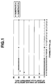
- FIG. 1 is a graph showing the number of concave defects versus etching depth.
- Silica glass substrates are generally manufactured by forming a quartz glass ingot in a conventional manner, shaping and annealing the ingot, slicing the ingot into slices, effecting rough polishing on the slices, then effecting precision polishing that determines the final surface quality.
- abrasive cloth and polishing compound are selected so as to give a desired finish surface. This is followed by cleaning, drying and etching, thereby completing silica glass substrates.
- the invention requires that when the substrate is treated with a reactive reagent, defects having a size of at least 0.3 ⁇ m in a direction parallel to the substrate major surface be absent on the substrate surface.
- the present invention selects those substrates in which defects with a size of at least 0.3 ⁇ m are not found on microscopic inspection after the finish surface is subjected to etching for causing latent damages, if any, to be manifested. That is, latent damage-free substrates are selected. This is because those silica glass substrates which have not manifested defects upon etching do generate no defects during the subsequent cleaning or etching step.
- Any desired chemical may be used for the etching treatment of the finish surface as long as it is reactive with silica glass.
- the preferred chemicals include fluoride ion-containing compounds such as conc. hydrofluoric acid, diluted hydrofluoric acid and buffered hydrofluoric acid.
- the chemical solution may contain a surfactant and a reaction control reagent. The chemical solution is preferably used under such conditions that uniform etching proceeds at an appropriate rate.
- substrates were immersed in hydrofluoric acid.
- the number of concave defects having a size of at least 0.3 ⁇ m is plotted as a function of an etching depth ( ⁇ m).
- the number of manifesting defects was saturated if immersion treatment was carried out so as to provide an etching depth of 0.2 ⁇ m or greater.
- further etching treatment with hydrofluoric acid does not cause defects to manifest (see data of substrate A in FIG. 1).
- the etching depth in FIG. 1 is the depth of material etched away with the etching chemical combined with the depth of material removed with the reactive reagent to be described later.
- the etching depth of silica glass substrate is preferably in the range of 0.2 ⁇ m to 0.5 ⁇ m.
- the defects that manifest when a silica glass substrate obtained by polishing, cleaning and etching a silica glass substrate slice is treated with a reactive reagent are defined as having a size of at least 0.3 ⁇ m in a direction parallel to the substrate major surface. This size is dependent on the detection ability of the existing defect inspection technique. It is readily understood that even when an inspection technique with a higher sensitivity is employed, the inventive method can comply with finer defects or latent damages by reconsidering the etching conditions.
- the reactive reagent includes the foregoing acidic or alkaline reagents in combination with a surfactant such as sodium alkylbenzenesulfonate, polyoxyethylene alkyl ether hydrogen sulfate or dioctylsulfosuccinate or a chelating agent such as sodium tripolyphosphate, sodium pyrophosphate, zeolite or sodium ethylenediamine tetraacetate.
- concave defects present on the substrate surface can be found by scanning the entire substrate surface under a microscope such as a stereomicroscope, and their shape and size be determined using an atomic force microscope.
- This inspection technique is capable of detecting concave defects with a size of at least 0.3 ⁇ m (see Japanese Patent No. 2,705,764).
- a quartz glass ingot shaped and annealed was sliced into 50 silica glass substrate slices having a diameter of 6 inches. After lapping and rough polishing, the slices proceeded to final precision polishing. Using abrasive cloth of suede type and a slurry of abrasive grains with a diameter of several tens of nanometers as the polishing slurry, polishing was done batchwise on either surface. The polishing step was followed by cleaning and drying. The slices were etched with a 1% aqueous hydrofluoric acid solution to a depth of 0.3 ⁇ m in a thickness direction. By scanning the entire surface of the resulting substrates under a stereomicroscope, forty five (45) substrates free of concave defects were picked up.
- the 45 defect-free substrates thus selected were treated with a 10% aqueous hydrofluoric acid solution for 10 minutes whereupon it was examined whether or not defects manifested. Upon inspection of these substrates under a stereomicroscope, defects manifested in none of the 45 substrates (rejection rate 0%).
Landscapes
- Chemical & Material Sciences (AREA)
- Engineering & Computer Science (AREA)
- Life Sciences & Earth Sciences (AREA)
- Chemical Kinetics & Catalysis (AREA)
- General Chemical & Material Sciences (AREA)
- Geochemistry & Mineralogy (AREA)
- Materials Engineering (AREA)
- Organic Chemistry (AREA)
- Mechanical Engineering (AREA)
- Surface Treatment Of Glass (AREA)
- Cleaning Or Drying Semiconductors (AREA)
- Preparing Plates And Mask In Photomechanical Process (AREA)
Abstract
Description
- This invention relates to silica glass substrates for use as the reticle belonging to the most advanced application among semiconductor-related electronic materials, expected to find spreading application in the microelectronics and microanalysis fields, and also for use as silica glass chips, and a method for selecting silica glass substrates.
- Quality requirements of reticle-forming silica glass substrates include the size and density of defects on substrates, the flatness and surface roughness of substrates, the photochemical stability of material, and the chemical stability of surface. Of these, the quality requirements concerning the on-substrate defects become more stringent on account of the recent trend toward further miniaturization of integrated circuits.
- The defective quality of reticle-forming silica glass substrates has been gradually improved. Currently, substrates in which concave defects with a size of less than about 0.3 µm are present are used. This is because the visual inspection under a collective lamp at a sufficient illuminance to avoid any hygienic problem and the defective inspection by an automatic defect detecting system have the technical limit that concave defects such as flaws are less sensitive than convex defects such as particles, and the probability to detect concave defects with a size of less than about 0.3 µm is very low. This inspection limit caused a delay in devising substrate quality improvements.
- Even in the substrates in which concave defects with a size of less than about 0.3 µm are apparently absent, chemical reagents used in cleaning and otherwise processing steps can cause enlargement of ultrafine concave defects and release of residual strains, giving rise to the problem that latent damages manifest themselves as defects.
- In the case of phase shift masks which are expected to become predominant in the next generation technology, the step of positively etching the silica glass surface is involved. It is problematic if latent damages on the substrate surface manifest themselves during the step.
- No substantial attention has been paid to the latent damages in quartz substrates which manifest themselves under the action of reactive reagents. Heretofore, polished substrates are regarded acceptable if no defects are found on the substrate surface. This is one of factors that make indefinite the cause for a substantial rejection rate of reticles.
- An object of the invention is to provide a silica glass substrate in which latent damages do not manifest themselves under the action of reactive reagents and concave defects having a size of at least 0.3 µm are absent. Another object of the invention is to provide a method of selecting such silica glass substrates.
- Using a silica glass substrate which is obtained by polishing a silica glass substrate slice, cleaning and etching, preferably to a depth of 0.2 to 0.5 µm in a thickness direction, and in which when treated with a reactive reagent, defects having a size of at least 0.3 µm in a direction parallel to the substrate major surface are absent on the substrate surface, the yield of semiconductor device manufacture and microelectronic system fabrication is improved.
- The invention provides a silica glass substrate obtained by polishing, cleaning, drying and etching a silica glass substrate slice. The substrate has a pair of major surfaces and a thickness therebetween. When the substrate is treated with a reactive reagent, defects having a size of at least 0.3 µm in a direction parallel to the substrate major surface are absent on the substrate surface.
- Preferably, in the etching step, the silica glass substrate slice is etched away in an amount of 0.2 to 0.5 µm in a thickness direction thereof. The reactive reagent is typically an acidic or alkaline reagent.
- Another aspect of the invention provides a method for selecting silica glass substrates, comprising the steps of polishing, cleaning, drying and etching silica glass substrate slices to form silica glass substrates, and inspecting the substrates for surface defects, thereby selecting those substrates on a surface of which defects having a size of at least 0.3 µm in a direction parallel to the substrate major surface are absent.
- The only figure, FIG. 1 is a graph showing the number of concave defects versus etching depth.
- Silica glass substrates are generally manufactured by forming a quartz glass ingot in a conventional manner, shaping and annealing the ingot, slicing the ingot into slices, effecting rough polishing on the slices, then effecting precision polishing that determines the final surface quality. In the precision polishing step, abrasive cloth and polishing compound are selected so as to give a desired finish surface. This is followed by cleaning, drying and etching, thereby completing silica glass substrates. The invention requires that when the substrate is treated with a reactive reagent, defects having a size of at least 0.3 µm in a direction parallel to the substrate major surface be absent on the substrate surface.
- In the above process of manufacturing silica glass substrates, use of only the precise polishing step, even when a desired finish surface is arrived at by using an appropriate combination of abrasive cloth and polishing compound, results in silica glass substrates with a certain probability of involving latent damages which will manifest themselves in the subsequent step of cleaning or etching.
- Then the present invention selects those substrates in which defects with a size of at least 0.3 µm are not found on microscopic inspection after the finish surface is subjected to etching for causing latent damages, if any, to be manifested. That is, latent damage-free substrates are selected. This is because those silica glass substrates which have not manifested defects upon etching do generate no defects during the subsequent cleaning or etching step.
- Any desired chemical may be used for the etching treatment of the finish surface as long as it is reactive with silica glass. The preferred chemicals include fluoride ion-containing compounds such as conc. hydrofluoric acid, diluted hydrofluoric acid and buffered hydrofluoric acid. The chemical solution may contain a surfactant and a reaction control reagent. The chemical solution is preferably used under such conditions that uniform etching proceeds at an appropriate rate.
- In one example, substrates were immersed in hydrofluoric acid. In the diagram of FIG. 1, the number of concave defects having a size of at least 0.3 µm is plotted as a function of an etching depth (µm). The number of manifesting defects was saturated if immersion treatment was carried out so as to provide an etching depth of 0.2 µm or greater. For the substrate in which no defects manifested in the immersion treatment, further etching treatment with hydrofluoric acid does not cause defects to manifest (see data of substrate A in FIG. 1). Inversely, when substrates are etched to a depth of less than 0.2 µm at which the number of manifesting defects has not been saturated, there is an increased probability of wrongly judging that the substrates are latent damage-free substrates (see data of substrate B in FIG. 1). It is noted that the etching depth in FIG. 1 is the depth of material etched away with the etching chemical combined with the depth of material removed with the reactive reagent to be described later.
- In either case, if the etching depth is more than 0.5 µm, no problem arises in theory, but the chemical solution used therefor runs to waste in a substantial sense and sometimes gives rise to extra problems such as the difficulty of uniform etching and surface roughening. Therefore, the etching depth of silica glass substrate is preferably in the range of 0.2 µm to 0.5 µm.
- In the context of the invention, the defects that manifest when a silica glass substrate obtained by polishing, cleaning and etching a silica glass substrate slice is treated with a reactive reagent are defined as having a size of at least 0.3 µm in a direction parallel to the substrate major surface. This size is dependent on the detection ability of the existing defect inspection technique. It is readily understood that even when an inspection technique with a higher sensitivity is employed, the inventive method can comply with finer defects or latent damages by reconsidering the etching conditions.
- The reactive reagent used herein includes acidic and alkaline chemicals used in cleaning and etching steps. Acidic reagents include fluoride ion-containing compounds such as hydrofluoric acid, buffered hydrofluoric acid, ammonium fluoride, ammonium monohydrogen difluoride, and borofluoric acid, as well as sulfuric acid, nitric acid, hydrochloric acid, acetic acid, citric acid, malic acid, oxalic acid, and perchloric acid, with the fluoride ion-containing compounds being especially preferred. Alkaline reagents include sodium hydroxide, potassium hydroxide, calcium hydroxide, ammonia and amines. Also included in the reactive reagent are the foregoing acidic or alkaline reagents in combination with a surfactant such as sodium alkylbenzenesulfonate, polyoxyethylene alkyl ether hydrogen sulfate or dioctylsulfosuccinate or a chelating agent such as sodium tripolyphosphate, sodium pyrophosphate, zeolite or sodium ethylenediamine tetraacetate. Further included are gases of carbon tetrafluoride, methane trifluoride, sulfur hexafluoride and hydrogen fluoride used in gas phase etching, known as dry etching.
- It is noted that concave defects present on the substrate surface can be found by scanning the entire substrate surface under a microscope such as a stereomicroscope, and their shape and size be determined using an atomic force microscope. This inspection technique is capable of detecting concave defects with a size of at least 0.3 µm (see Japanese Patent No. 2,705,764).
- Examples of the invention and comparative examples are given below by way of illustration, and not by way of limitation. The parameters used in the examples are not intended to restrict the scope of the invention.
- A quartz glass ingot shaped and annealed was sliced into 50 silica glass substrate slices having a diameter of 6 inches. After lapping and rough polishing, the slices proceeded to final precision polishing. Using abrasive cloth of suede type and a slurry of abrasive grains with a diameter of several tens of nanometers as the polishing slurry, polishing was done batchwise on either surface. The polishing step was followed by cleaning and drying. The slices were etched with a 1% aqueous hydrofluoric acid solution to a depth of 0.3 µm in a thickness direction. By scanning the entire surface of the resulting substrates under a stereomicroscope, forty five (45) substrates free of concave defects were picked up.
- The 45 defect-free substrates thus selected were treated with a 10% aqueous hydrofluoric acid solution for 10 minutes whereupon it was examined whether or not defects manifested. Upon inspection of these substrates under a stereomicroscope, defects manifested in none of the 45 substrates (
rejection rate 0%). - Forty five (45) silica glass substrate slices having a diameter of 6 inches produced as above were subjected to lapping and rough polishing, then to final precision polishing. Using abrasive cloth of suede type and a slurry of abrasive grains with a diameter of several tens of nanometers as the polishing slurry, polishing was done batchwise on either surface. The polishing step was followed by cleaning and drying. Without etching with a 1% aqueous hydrofluoric acid solution as in Example 1, the 45 substrates were examined whether or not defects manifested by treatment with a 10% aqueous hydrofluoric acid solution. Upon inspection of the substrates under a stereomicroscope, defects manifested in five of the 45 substrates (rejection rate 11%).
- There have been described silica glass substrates which are advantageous for use as the reticle in the photolithographic process for the fabrication of integrated circuits in that fine defects with a size of 0.3 µm or greater do not manifest on the substrate surface even when processed as by cleaning and etching, so that the yield of semiconductor device manufacture and microelectronic system fabrication is improved.
- Japanese Patent Application No. 2000-397364 is incorporated herein by reference.
- Although some preferred embodiments have been described, many modifications and variations may be made thereto in light of the above teachings. It is therefore to be understood that the invention may be practiced otherwise than as specifically described without departing from the scope of the appended claims.
Claims (6)
- A silica glass substrate obtained by polishing, cleaning, drying and etching a silica glass substrate slice, said substrate having a pair of major surfaces and a thickness therebetween, in which when the substrate is treated with a reactive reagent, defects having a size of at least 0.3 µm in a direction parallel to the substrate major surface are absent on the substrate surface.
- The silica glass substrate of claim 1 wherein in the etching step, the silica glass substrate slice is etched away in an amount of 0.2 to 0.5 µm in a thickness direction thereof.
- The silica glass substrate of claim 1 wherein the reactive reagent is an acidic or alkaline reagent.
- A method for selecting silica glass substrates, comprising the steps of polishing, cleaning, drying and etching silica glass substrate slices to form silica glass substrates, and inspecting the substrates for surface defects, thereby selecting those substrates on a surface of which defects having a size of at least 0.3 µm in a direction parallel to the substrate major surface are absent.
- The method for selecting silica glass substrates of claim 4, wherein in the etching step, the silica glass substrate slices are etched away in an amount of 0.2 to 0.5 µm in a thickness direction thereof.
- A silica glass substrate selected by the method of claim 4 or claim 5.
Applications Claiming Priority (2)
| Application Number | Priority Date | Filing Date | Title |
|---|---|---|---|
| JP2000397364 | 2000-12-27 | ||
| JP2000397364A JP3874066B2 (en) | 2000-12-27 | 2000-12-27 | Selection method of silica glass substrate |
Publications (2)
| Publication Number | Publication Date |
|---|---|
| EP1219575A1 true EP1219575A1 (en) | 2002-07-03 |
| EP1219575B1 EP1219575B1 (en) | 2009-01-14 |
Family
ID=18862496
Family Applications (1)
| Application Number | Title | Priority Date | Filing Date |
|---|---|---|---|
| EP01310754A Expired - Lifetime EP1219575B1 (en) | 2000-12-27 | 2001-12-21 | Method for the selection of silica glass substrates |
Country Status (4)
| Country | Link |
|---|---|
| US (1) | US6928837B2 (en) |
| EP (1) | EP1219575B1 (en) |
| JP (1) | JP3874066B2 (en) |
| DE (1) | DE60137401D1 (en) |
Cited By (2)
| Publication number | Priority date | Publication date | Assignee | Title |
|---|---|---|---|---|
| WO2004008247A1 (en) * | 2002-07-17 | 2004-01-22 | Hoya Corporation | Glass substrate for mask blank and method of producing the same |
| EP2781880A1 (en) | 2013-03-19 | 2014-09-24 | Leica Geosystems AG | Construction laser system with at least partially automatic recalibration functionality for a beam leveling function |
Families Citing this family (9)
| Publication number | Priority date | Publication date | Assignee | Title |
|---|---|---|---|---|
| JP4170569B2 (en) * | 2000-06-02 | 2008-10-22 | 大日本印刷株式会社 | Board selection device |
| AUPQ922000A0 (en) * | 2000-08-04 | 2000-08-31 | Bae Systems Australia Limited | Method of constructing an optical parametric oscillator |
| TWI250133B (en) * | 2002-01-31 | 2006-03-01 | Shinetsu Chemical Co | Large-sized substrate and method of producing the same |
| KR100556141B1 (en) * | 2003-03-27 | 2006-03-03 | 호야 가부시키가이샤 | Method of producing a glass substrate for a mask blank and method of producing a mask blank |
| KR20100007461A (en) * | 2008-07-14 | 2010-01-22 | 삼성전자주식회사 | Cleaning solution for quartz part and method of cleaning using the same |
| JP5251861B2 (en) * | 2009-12-28 | 2013-07-31 | 信越化学工業株式会社 | Method for producing synthetic quartz glass substrate |
| KR101353525B1 (en) * | 2010-02-09 | 2014-01-21 | 주식회사 엘지화학 | Lay-out for system of manufacturing glass, method for handling glass and glass therefrom |
| US20130130508A1 (en) * | 2011-09-02 | 2013-05-23 | Air Products And Chemicals, Inc. | Compositions and Methods for Texturing of Silicon Wafers |
| JP6173733B2 (en) * | 2012-03-23 | 2017-08-02 | Hoya株式会社 | Mask blank, transfer mask, and manufacturing method thereof |
Citations (4)
| Publication number | Priority date | Publication date | Assignee | Title |
|---|---|---|---|---|
| US4274907A (en) * | 1980-05-08 | 1981-06-23 | The United States Of America As Represented By The Secretary Of The Army | Method of chemically polishing a doubly rotated quartz plate |
| USH532H (en) * | 1986-10-20 | 1988-10-04 | The United States Of America As Represented By The Secretary Of The Army | Method of chemically polishing fused quartz |
| JPH11335140A (en) * | 1998-05-26 | 1999-12-07 | Toshiba Ceramics Co Ltd | Production of optical synthetic quartz glass |
| JP2000302482A (en) * | 1999-04-23 | 2000-10-31 | Nippon Sheet Glass Co Ltd | Production method of glass substrate and glass substrate for magnetic recording medium obtained by the method |
Family Cites Families (1)
| Publication number | Priority date | Publication date | Assignee | Title |
|---|---|---|---|---|
| FR2706445B1 (en) * | 1993-06-18 | 1995-09-08 | Holophane | Method for manufacturing lighthouse ice, ice thus obtained and mold for the implementation of this method. |
-
2000
- 2000-12-27 JP JP2000397364A patent/JP3874066B2/en not_active Expired - Fee Related
-
2001
- 2001-12-21 DE DE60137401T patent/DE60137401D1/en not_active Expired - Lifetime
- 2001-12-21 EP EP01310754A patent/EP1219575B1/en not_active Expired - Lifetime
- 2001-12-27 US US10/026,462 patent/US6928837B2/en not_active Expired - Lifetime
Patent Citations (4)
| Publication number | Priority date | Publication date | Assignee | Title |
|---|---|---|---|---|
| US4274907A (en) * | 1980-05-08 | 1981-06-23 | The United States Of America As Represented By The Secretary Of The Army | Method of chemically polishing a doubly rotated quartz plate |
| USH532H (en) * | 1986-10-20 | 1988-10-04 | The United States Of America As Represented By The Secretary Of The Army | Method of chemically polishing fused quartz |
| JPH11335140A (en) * | 1998-05-26 | 1999-12-07 | Toshiba Ceramics Co Ltd | Production of optical synthetic quartz glass |
| JP2000302482A (en) * | 1999-04-23 | 2000-10-31 | Nippon Sheet Glass Co Ltd | Production method of glass substrate and glass substrate for magnetic recording medium obtained by the method |
Non-Patent Citations (5)
| Title |
|---|
| "PHASE SHIFT MASK FABRICATION USING REACTIVE ION ETCHING OF QUARTZ SUBSTRATES", RESEARCH DISCLOSURE, KENNETH MASON PUBLICATIONS, HAMPSHIRE, GB, no. 340, 1 August 1992 (1992-08-01), pages 682, XP000324137, ISSN: 0374-4353 * |
| DATABASE INSPEC [online] INSTITUTE OF ELECTRICAL ENGINEERS, STEVENAGE, GB; TAKEUCHI M ET AL: "Properties of our developing next generation photomask substrate", XP002194301, Database accession no. 6584331 * |
| PATENT ABSTRACTS OF JAPAN vol. 2000, no. 03 30 March 2000 (2000-03-30) * |
| PATENT ABSTRACTS OF JAPAN vol. 2000, no. 13 5 February 2001 (2001-02-05) * |
| PHOTOMASK AND X-RAY MASK TECHNOLOGY VI, YOKOHAMA, JAPAN, 13-14 APRIL 1999, vol. 3748, Proceedings of the SPIE - The International Society for Optical Engineering, 1999, SPIE-Int. Soc. Opt. Eng, USA, pages 41 - 52, ISSN: 0277-786X * |
Cited By (2)
| Publication number | Priority date | Publication date | Assignee | Title |
|---|---|---|---|---|
| WO2004008247A1 (en) * | 2002-07-17 | 2004-01-22 | Hoya Corporation | Glass substrate for mask blank and method of producing the same |
| EP2781880A1 (en) | 2013-03-19 | 2014-09-24 | Leica Geosystems AG | Construction laser system with at least partially automatic recalibration functionality for a beam leveling function |
Also Published As
| Publication number | Publication date |
|---|---|
| JP3874066B2 (en) | 2007-01-31 |
| JP2002201042A (en) | 2002-07-16 |
| US6928837B2 (en) | 2005-08-16 |
| EP1219575B1 (en) | 2009-01-14 |
| DE60137401D1 (en) | 2009-03-05 |
| US20020078710A1 (en) | 2002-06-27 |
Similar Documents
| Publication | Publication Date | Title |
|---|---|---|
| EP2007691B1 (en) | Processing method of glass substrate, and highly flat and highly smooth glass substrate | |
| KR101118004B1 (en) | Methods of finishing quartz glass surfaces and components made by the methods | |
| US6928837B2 (en) | Silica glass substrates and their selection | |
| EP2338849A1 (en) | Preparation of synthetic quartz glass substrates | |
| US7517706B2 (en) | Method for evaluating quality of semiconductor substrate and method for manufacturing semiconductor substrate | |
| CN114813808B (en) | Method for detecting cross-sectional structure of semiconductor chip | |
| US6600557B1 (en) | Method for the detection of processing-induced defects in a silicon wafer | |
| EP1084510A1 (en) | Post-etching alkaline treatment process | |
| US6849548B2 (en) | Method of reducing particulate contamination during polishing of a wafer | |
| US6530381B1 (en) | Process for the wet-chemical surface treatment of a semiconductor wafer | |
| US7479204B2 (en) | Method of manufacturing semiconductor substrate and method of evaluating quality of semiconductor substrate | |
| JPH05226203A (en) | Mirror-surface wafer, its manufacture and its inspection method | |
| JP3441979B2 (en) | Semiconductor wafer processing method and semiconductor wafer | |
| KR101275384B1 (en) | Method of processing silicon wafer | |
| JP2000208578A (en) | Evaluation method for silicon wafer and silicon wafer | |
| JP2005203507A (en) | Semiconductor wafer processing method and semiconductor wafer treating apparatus | |
| JP7279753B2 (en) | Silicon wafer cleaning method and manufacturing method | |
| KR100211648B1 (en) | Semiconductor Wafer Recycling Method | |
| CN113043159A (en) | Method for polishing silicon wafer | |
| JP3890981B2 (en) | Alkaline etching solution, method for etching silicon wafer using this etching solution, and method for differentiating front and back surfaces of silicon wafer using this method | |
| JP7571691B2 (en) | Silicon wafer cleaning method and manufacturing method, and method for evaluating hydrogen peroxide concentration in cleaning solution and method for managing hydrogen peroxide concentration | |
| JPH11330042A (en) | Inspection for specularly beveled part of silicon wafer | |
| JPH11251273A (en) | Method for manufacturing semiconductor integrated circuit device, method for manufacturing semiconductor wafer, and semiconductor wafer | |
| JPH10112486A (en) | Method of measuring oxide film dielectric strength of semiconductor wafer | |
| JPH08167640A (en) | Semiconductor substrate for foreign matter management |
Legal Events
| Date | Code | Title | Description |
|---|---|---|---|
| PUAI | Public reference made under article 153(3) epc to a published international application that has entered the european phase |
Free format text: ORIGINAL CODE: 0009012 |
|
| AK | Designated contracting states |
Kind code of ref document: A1 Designated state(s): AT BE CH CY DE DK ES FI FR GB GR IE IT LI LU MC NL PT SE TR |
|
| AX | Request for extension of the european patent |
Free format text: AL;LT;LV;MK;RO;SI |
|
| 17P | Request for examination filed |
Effective date: 20020909 |
|
| AKX | Designation fees paid |
Designated state(s): DE FR GB |
|
| 17Q | First examination report despatched |
Effective date: 20030617 |
|
| GRAP | Despatch of communication of intention to grant a patent |
Free format text: ORIGINAL CODE: EPIDOSNIGR1 |
|
| GRAC | Information related to communication of intention to grant a patent modified |
Free format text: ORIGINAL CODE: EPIDOSCIGR1 |
|
| RTI1 | Title (correction) |
Free format text: METHOD FOR THE SELECTION OF SILICA GLASS SUBSTRATES |
|
| GRAS | Grant fee paid |
Free format text: ORIGINAL CODE: EPIDOSNIGR3 |
|
| GRAA | (expected) grant |
Free format text: ORIGINAL CODE: 0009210 |
|
| AK | Designated contracting states |
Kind code of ref document: B1 Designated state(s): DE FR GB |
|
| REG | Reference to a national code |
Ref country code: GB Ref legal event code: FG4D |
|
| REF | Corresponds to: |
Ref document number: 60137401 Country of ref document: DE Date of ref document: 20090305 Kind code of ref document: P |
|
| PLBE | No opposition filed within time limit |
Free format text: ORIGINAL CODE: 0009261 |
|
| STAA | Information on the status of an ep patent application or granted ep patent |
Free format text: STATUS: NO OPPOSITION FILED WITHIN TIME LIMIT |
|
| 26N | No opposition filed |
Effective date: 20091015 |
|
| REG | Reference to a national code |
Ref country code: FR Ref legal event code: PLFP Year of fee payment: 15 |
|
| REG | Reference to a national code |
Ref country code: FR Ref legal event code: PLFP Year of fee payment: 16 |
|
| REG | Reference to a national code |
Ref country code: FR Ref legal event code: PLFP Year of fee payment: 17 |
|
| PGFP | Annual fee paid to national office [announced via postgrant information from national office to epo] |
Ref country code: DE Payment date: 20191210 Year of fee payment: 19 |
|
| PGFP | Annual fee paid to national office [announced via postgrant information from national office to epo] |
Ref country code: FR Payment date: 20191115 Year of fee payment: 19 |
|
| PGFP | Annual fee paid to national office [announced via postgrant information from national office to epo] |
Ref country code: GB Payment date: 20191219 Year of fee payment: 19 |
|
| REG | Reference to a national code |
Ref country code: DE Ref legal event code: R119 Ref document number: 60137401 Country of ref document: DE |
|
| GBPC | Gb: european patent ceased through non-payment of renewal fee |
Effective date: 20201221 |
|
| PG25 | Lapsed in a contracting state [announced via postgrant information from national office to epo] |
Ref country code: FR Free format text: LAPSE BECAUSE OF NON-PAYMENT OF DUE FEES Effective date: 20201231 |
|
| PG25 | Lapsed in a contracting state [announced via postgrant information from national office to epo] |
Ref country code: DE Free format text: LAPSE BECAUSE OF NON-PAYMENT OF DUE FEES Effective date: 20210701 Ref country code: GB Free format text: LAPSE BECAUSE OF NON-PAYMENT OF DUE FEES Effective date: 20201221 |