The present invention refers to a process for manufacturing
integrated devices having connections on a separate wafer, and
to an integrated device thus obtained.
As is known, standard processes for manufacturing integrated
circuits involve carrying out individual process steps in a
sequential way. The manufacture of micro-integrated structures
(so-called micro-electromechanical systems, or MEMS) and their
control circuits in a same monolithic device has required a
certain number of manufacture steps for defining the micro-integrated
structures within the process of manufacturing
traditional electronic components, with an increase in
complexity which is not always sustainable. Consequently, in
many cases the choice is made to carry out parallel
manufacturing processes to obtain, on one hand, the control
circuits, and, on the other, the micro-integrated structures,
and at a certain point to bond the obtained structures, so
that the two processes may involve only a few non-critical
common steps.
Thereby, it is possible to continue to exploit the potential
of planar technology (batch-type processes), whilst the
minimum time required for obtaining a finished device (so-called
"cycle time") is markedly reduced. In addition, with
parallel processing, it is possible to separate parts and
processing steps that could lead to contamination.
Recently a manufacturing process has been proposed (see US-A-5,736,395)
based upon parallel manufacture of a first
substrate housing an integrated circuit and a second substrate
comprising the interconnections for the integrated circuit,
and bonding the two substrates together in the final
manufacturing steps.
The separation of the operations for forming the integrated
components in a silicon substrate from the operations for
forming interconnections enables a simplification of the
process as a whole.
In the parallel process proposed, bonding of the two
substrates is obtained by forming, on both substrates,
appropriate metal contact regions coated with a bonding layer
of a low-melting alloyable metal, for example gold or
palladium.
The need to include steps for depositing and defining the
metal contact regions and the bonding layer on top of both
substrates is, however, disadvantageous in so far as it does
not enable separation of the operations for forming components
integrated in the silicon from the metallurgical operations
for forming interconnections. Consequently, the techniques for
forming the interconnections risk affecting the components
that belong to the integrated circuit and may give rise to
undesired charging phenomena or to contamination.
In addition, the described parallel process requires forming
through holes in the substrate carrying the interconnections
for aligning the two substrates in the bonding step, with an
increase in costs and in manufacturing times for forming the
corresponding masks and the holes.
The aim of the present invention is therefore to provide a
parallel manufacturing process that eliminates the need to
form contact regions and a bonding layer on both substrates,
so as to keep the metallurgical operations completely separate
from the operations for forming integrated components of
semiconductor or insulating material, and to simplify the
operations for bonding the two substrates.
According to the present invention, a process is provided for
manufacturing integrated devices, as well as an integrated
device thus obtained, as defined in Claim 1 and Claim 13,
respectively.
For a better understanding of the present invention, preferred
embodiments thereof are now described, purely to provide nonlimiting
examples, with reference to the attached drawings,
wherein:
- Figure 1 shows a cross-section of a first wafer housing
electronic components for implementing the parallel
manufacturing process according to the invention;
- Figure 2 shows a cross-section of a second wafer housing
interconnections for the components of Figure 1;
- Figure 3 shows a cross-section of a composite wafer obtained
by bonding the wafers of Figures 1 and 2;
- Figure 4 shows a cross-section of the composite wafer of
Figure 3, in a subsequent step of the manufacturing process;
- Figure 5 presents a detail of an alignment structure made on
the wafer of Figure 1;
- Figure 6 presents a detail of a corresponding alignment
structure made on the wafer of Figure 2;
- Figure 7 shows details of Figures 5 and 6 after alignment
and bonding of the two substrates;
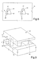
- Figure 8 is a top view of the alignment structure of Figure
5;
- Figure 9 is a perspective view of the step of aligning the
structures of Figures 5 and 6;
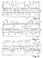
- Figure 10 shows a cross-section of a first MEMS device
formed using the parallel fabrication technique according to
the invention;
- Figure 11 shows a cross-section of a second MEMS device
formed using the parallel fabrication technique according to
the invention;
- Figure 12 shows a cross-section of a third MEMS device
formed using the parallel fabrication technique according to
the invention;
- Figures 13-15 show cross-sections of a first wafer used for
manufacturing the third MEMS device according to Figure 11, in
successive steps; and
- Figure 16 shows a cross-section of a composite wafer
obtained by bonding the wafer of Figure 15 to a wafer housing
interconnections, in an advanced manufacturing step.
Figure 1 shows a cross-section of a first wafer 1 housing
electronic components belonging to an integrated electronic
circuit. In particular, the first wafer 1 comprises a
substrate 2 having a surface 2a and housing a bipolar
transistor 3 and a PMOS transistor 4, each formed in an own
well 5, 6 isolated from one another by junction isolation
regions 7. The well 5 accommodates a collector contact region
10 and a base region 11, and the base region 11 houses a base
contact region 12 and an emitter region 13. The well 6
accommodates source regions 14. In addition, isolation contact
regions 15 are formed inside the junction isolation region 7.
The collector contact region 10, base region 11, base contact
region 12, emitter region 13, source regions 14, and isolation
contact regions 15 face the surface 2a of the substrate 2. A
dielectric protection layer 18 extends on top of the surface
2a of the substrate 2 and has openings 19 at the regions 10,
and 12-15. A gate region 20, of polycrystalline silicon,
extends in part on top of the surface 2a and in part in a
depression inside the substrate 2, and is electrically
insulated from the substrate 2 by the dielectric protection
layer 18.
The first wafer 1 is obtained via standard process steps,
which are not described in detail herein.
Figure 2 shows a cross-section of a second wafer 25 comprising
interconnection regions intended for the first wafer 1 of
Figure 1. In particular, the second wafer 25 comprises a
substrate 26 of monocrystalline silicon, covered by an oxide
layer 27. Two metal levels are formed on top of the oxide
layer 27 and comprise first connection regions 28 on top of
the oxide layer 27 and second connection regions 30 on top of
the first connection regions 28 and insulated therefrom by an
insulating layer 31. Through connections 29 extend through the
insulating layer 31 and selectively connect some of the first
connection regions 28 to some of the second connection regions
30. Plug elements 32 are formed on top of the second
connection regions 30 at the openings 19 and the gate region
20 of the first wafer 1. The plug elements 32 preferably
comprise a base region 33, for example of aluminum, and a
bonding region 34, of a metal capable of reacting with silicon
to form a silicide, such as titanium, palladium, nickel,
platinum, tungsten, and cobalt.
The second wafer 25 is preferably obtained as follows:
initially the oxide layer 27 is deposited or grown on top of
the substrate 26; then a first metal layer is deposited and
defined so as to form the first connection regions 28; the
insulating layer 31 is deposited; openings are formed in the
insulating layer 31 where the through connections 29 are to be
made; a second metal layer is deposited and removed from on
top of the insulating layer 31; then a third metal layer is
deposited and defined so as to form the second connection
regions 30; next, a fourth metal layer and a metal layer
capable of reacting with silicon are deposited and defined so
as to form the plug elements 32. The first and second
connection regions 28, 30 and the through connections 29 are
made of any suitable metal, even one not necessarily
compatible with processing of silicon, such as silver and
copper.
Next (Figure 3), the second wafer 25 is turned upside down on
top of the wafer 1 so that the top ends of the plug regions 32
insert into the corresponding openings 19, and, by applying an
appropriate temperature (of at least 230°C, according to the
type of metal capable of reacting with silicon) and a small
pressure, the bonding regions 34 are made to react with the
uncovered silicon through the openings 19 or with the
polycrystalline silicon of the gate region 20 to form metal
silicide which is conductive and stable over time. In this
way, a composite wafer 36 is formed.
In order to guarantee the reaction of the bonding regions 34,
the silicon exposed at the openings 19 and the polycrystalline
silicon of the gate region 20 are preferably cleaned with
gaseous anhydrous hydrofluoric acid, and all the silicon
regions that are bonded to the plug regions (regions 10 and
12-15, and portion of the gate region 20 on which the contact
is made) are on the same level.
Finally (Figure 4), the second wafer 25 is thinned, for
example by lapping, by removing the substrate 26 as far as the
oxide layer 27; then the oxide layer 27 is opened in order to
enable selective connection of some of the first connection
regions 28 with the outside. Alternatively, it is possible to
thin the second wafer 25 to arrive near to the oxide layer 27,
without, however, reaching the latter. Then, in the remaining
portion of the substrate 26, openings are formed at the pads
and traverse also the oxide layer 27, and connection wires are
then bonded.
The gap between the first wafer 1 and the second wafer 25
forms an insulation gap 37 having a low dielectric constant
and is filled with air or nitrogen, or else is set in vacuum
conditions (in the latter two cases, bonding may be performed
in a controlled environment as regards gas/pressure, and
annular plug elements 32 may be provided which surround the
active regions of each device into which the composite wafer
36 will then be divided, so as to seal the insulation gap 37
of each device from the external environment).
The advantages of the above described process are illustrated
hereinafter. First, parallel processing allows a reduction in
the cycle time, since the steps for manufacturing the second
wafer can be carried out even simultaneously with, or in any
case independently of, the steps for processing the first
wafer.
Since the plug elements 32 belonging to the second wafer 25
are bonded directly to silicon regions belonging to the first
wafer 1, the metallurgical operations for forming the
connection regions are completely independent of the
operations necessary for processing silicon; consequently,
there is no interference whatsoever between such operations.
The areas in which the two wafers are made may be separate;
consequently, for forming the connections it is possible to
use materials that are incompatible with silicon processing,
without any risk of contamination.
As far as the interconnections are concerned, it is possible
to proceed from the simpler levels (top levels) to the more
complex levels (bottom levels, including the first level which
is connected directly to silicon), so increasing the
sturdiness of the processes.
According to another aspect of the invention, in order to
facilitate alignment of the second wafer 25 to the first wafer
1, self-alignment structures are made, as is shown in Figures
5-9, where only one portion of the wafers 1, 25 is
illustrated.
In detail (Figures 5 and 6), the self-alignment structures
comprise engagement seats 40 formed in the first wafer 1 and
engagement elements 41 formed on the second wafer 25.
Specifically, as may be better seen from Figures 8 and 9, an
engagement seat 40 comprises a guide opening 42 in the
protective dielectric layer 18, having a trapezium shape, and
a notch 43 in the substrate 2, also having a trapezium shape
and with the minor base and the legs substantially aligned,
respectively, to the minor base and part of the legs of the
guide opening 42. The guide opening 42 has a much greater
length (height of the trapezium) than the notch 43.
The engagement seats 40 are obtained as follows: using an
appropriate mask or the mask for digging in the silicon used
to form the depression 21, the notch 43 is initially dug;
then, simultaneously and using the same mask as for the
openings 19, the guide opening 42 is dug. In this way, the
guide opening 42 is positioned precisely with respect to the
openings 19.
The engagement elements 41 preferably include two pins 44 for
each engagement seat 40, as may be seen in detail in Figures 8
and 9. The two pins 44 are arranged adjacent each other and
have dimensions and position such as to engage a corresponding
notch 43. The two pins 44 of each engagement element 41 are
formed on top of a second connection region (which, in actual
fact, does not have any function of electrical connection),
and each of them comprises a bottom region 45, which may be
made of any suitable material (for example, but not
necessarily, of the same material as the base regions 33 of
the plug elements 32), an intermediate region 46, formed
together with and made of the same material as the base
regions 33, and a top region 47, formed together with and made
of the same material as the bonding regions 34.
Since the pins 44 comprise one region more than the plug
elements 32, namely, the bottom region 45, they have a greater
height than the plug elements 32 themselves, namely by an
amount corresponding to the thickness of the bottom region 45.
The pins 44 are preferably formed as follows: a raising layer
is deposited on top of the second connection regions 30 and is
then removed everywhere, except where the pins 44 are to be
formed, using an appropriate mask. In this step, raising
regions are formed having dimensions that may not even
coincide with those of the bottom regions 45, but may be of
larger dimensions, in particular if the material of the bottom
regions 45 is the same as that of the intermediate regions 46.
Next, the fourth metal layer and the metal layer capable of
reacting with silicon are deposited and defined, so as to form
simultaneously the plug elements 32 and the intermediate
regions 46 and top regions 47. If the material of the raising
regions is the same as the fourth metal layer, also the bottom
regions 45 are defined in this step, even though this is not
always indispensable.
When the second wafer 25 is turned upside down on top of the
first wafer 1, it is roughly aligned in order to insert the
pins 44 into the guide openings 42 next to the major bases of
the trapeziums, as shown in Figure 8 with a solid line, and in
Figure 9. Next, the second wafer 25 is displaced laterally
with respect to the first wafer 1 in the direction indicated
by the arrows A, until the pairs of pins 44 insert into the
corresponding notches 43, thus causing the second wafer 25 to
collapse towards the first wafer 1 and the plug elements 32 to
engage the corresponding openings 19. Preferably, the height
of the pins 44 and the depth of the notches 43 is chosen in
such a way that the pins 44 do not touch the bottom of the
notches 43, so as to guarantee that, even in the presence of
process imprecisions, the plug elements 32 are always and
securely in contact with the substrate 2 and the gate region
20 of the first wafer 1.
Lateral movement of the second wafer 25 ends when the two pins
44 of each engagement element 41 both interfere with the legs
of the guide openings 42 and possibly of the notches 43,
fittedly engaged, as shown by the dashed lines in Figure 8,
and so guaranteeing excellent alignment of the wafers 1 and
25.
Figure 10 shows a device 50 formed by a first chip 51 housing
a micro-electromechanical structure 61 and a second chip 52
housing electrical connection regions.
In detail, the first chip 51 comprises a first substrate 54 of
monocrystalline silicon, a first insulating layer 55, for
example of silicon dioxide, and an epitaxial layer 56 of
polycrystalline silicon. The epitaxial layer 56 houses the
micro-electromechanical structure 61, including a rotor 57, a
stator 58, and biasing regions 59. The first insulating layer
55 has been removed from beneath the rotor 57 where an air gap
60 is formed in order to enable movement of the rotor 57,
which is supported by spring elements (not shown) in a per se
known manner.
The second chip 52 comprises a second substrate 65, of
monocrystalline silicon, a second insulating layer 66, of
silicon dioxide, a third insulating layer 67, of silicon
nitride, and plug elements 68, each of which includes a base
region 69, for example of aluminum, and a bonding region 70,
of silicide, such as titanium silicide, palladium silicide,
nickel silicide, platinum silicide, tungsten silicide, and
cobalt silicide.
The second substrate 65 has through openings 74 at some plug
elements 68. Underneath the through openings 74 also the
second insulating layer 66 and the third insulating layer 67
are removed. Thereby, the corresponding base regions 69 are
accessible from behind and are connected to electrical
connection wires 75 soldered through a gold ball (gold-wire
bonding technique).
The device 50 is formed as follows: the first insulating layer
55 is deposited or grown on a first wafer of crystalline
silicon (forming the first substrate 54); next, a thin layer
of polycrystalline silicon is deposited, and an epitaxial
layer 56 is grown. Alternatively, it is possible to use a SOI
wafer. Using a trench mask, micro-electromechanical structures
61 are defined; then the first insulating layer 55 is removed
from beneath the rotor 57.
Separately, the second insulating layer 66 is deposited or
grown on a second silicon wafer (forming the substrate 65).
The third insulating layer 67 is deposited. Using an
appropriate mask, openings are formed in the third insulating
layer 67. Then a metal layer, for example of aluminum, is
deposited and defined to form the base regions 69. A layer of
a metal capable of reacting with silicon is deposited and
defined to form the bonding regions 70. Possibly, using an
appropriate etching technique, the base regions 69 and the
bonding regions 70 can be defined together using a single
mask. Next, using an appropriate mask, positioning structures,
for example notches, are formed on the rear of the second
wafer, i.e., on the side opposite that on which the second
insulating layer 66 and the third insulating layer 67 have
been formed.
Subsequently, the second wafer is turned upside down on the
first wafer, using the positioning structures present on the
rear of the second wafer and possibly exploiting the technique
of precise self-alignment described with reference to Figures
6-9. Subsequently, by heating to an appropriate temperature
and applying a small pressure, the bonding regions 70 are
soldered on the corresponding regions (here, the stator 58 and
the biasing regions 59) of the micro-electromechanical
structures 61, forming metal silicide. The second wafer is
thinned, for example by milling, down to a thickness of
between 50 and 100 µm, and, using an appropriate mask, the
through openings 74 are formed. Then the portions of the
second insulating layer 66 at the through openings 74 are
removed, thus uncovering from the rear the base regions 69,
which must be accessible for bonding. The composite wafer thus
obtained is then cut into dice and positioned where required,
and the electrical connection wires 75 are soldered.
Figure 11 shows a device 80 including a first chip 81, similar
to the first chip 51 of Figure 10 (and hence its parts are
designated by the same reference numbers and will not be
further described herein), and a second chip 82 housing
electrical connection regions obtained using the technique of
silicon plugs.
The second chip 82 comprises a silicon substrate 83
accommodating through connection regions 84, having
conductivity N+ and insulated from the rest of the substrate
83 by annular insulation regions 85 of silicon dioxide. A top
silicon layer 86 covers the rear of the substrate 83, and a
bottom oxide layer 87 covers the front of the substrate 83.
Plug regions 68, similar to the plug regions 68 of Figure 10,
join the second chip 82 to the first chip 81. Some of the plug
regions 68 are in electrical contact with the through
connection regions 84 and extend through corresponding
openings present in the bottom oxide layer 87.
Electrical connection regions 90, for example of aluminum,
extend over of the top oxide layer 86 and are in electrical
contact with the through connection regions 84 through
openings made in the top oxide layer 86. A protection layer
91, of silicon nitride, covers the electrical connection
regions 90 and the top oxide layer 86, except for openings
where electrical connection wires 92 are soldered to the
electrical connection regions 90 through gold-wire bonding.
The device 80 is manufactured as described hereinafter. A
first wafer, accommodating the first chip 81, is formed as
described previously in connection with Figure 10. The second
chip 82 is manufactured from a second wafer comprising a
monocrystalline-silicon sacrificial substrate, the top oxide
layer 86, and the substrate 83, for example a SOI wafer or a
wafer obtained by epitaxial growth starting from a polysilicon
germ layer deposited over the top oxide layer 86.
Using a deep trench mask, the substrate 83 is etched as far as
the top oxide layer 86. Then an oxide layer is deposited and
fills the trenches just obtained and forms the annular
insulation regions 85 and the bottom oxide layer 87. After
possible planarization of the bottom oxide layer 87, using an
appropriate mask openings are formed in the bottom oxide layer
87, so as to uncover the substrate 83 at the through
connection regions 84. Next, plug regions 68 are formed as
described above. As previously, using an appropriate mask,
positioning structures (notches) are made on the rear of the
second wafer.
Next, the second wafer is turned upside down, aligned and
bonded to the first wafer, as above described, for example in
a controlled environment. Subsequently, the second wafer is
thinned by completely removing the sacrificial layer until the
top oxide layer 86 is uncovered. Using an appropriate mask,
openings are formed in the top oxide layer 86. A metal layer,
for example of aluminum, is deposited and defined to form
electrical connection regions 90. The protection layer 91 is
deposited and defined. The wafer is cut into dice, and the
electrical connection wires 92 are formed. Alternatively, deep
trenches are formed in the second wafer and are filled with
insulating material deposited to form the annular insulation
regions 85 and the bottom oxide layer 87. The second wafer is
turned upside down and bonded to the first wafer; then it is
reduced in thickness until the annular insulation regions are
reached from the rear. Next, the top oxide layer 86, the
electrical connection regions 90, and the protection layer 91
are formed. Finally, the composite wafer is cut into dice, and
the electrical connection wires 92 are made.
Figure 12 shows a device 100 including a first chip 101,
similar to the first chip 51 of Figure 10 (and hence its parts
are designated by the same reference numbers and will not be
further described herein), and a second chip 102 housing
electrical connection regions which are directly accessible.
The first chip 101 has a smaller area than the second chip
102, so that the chip 102 projects on one side beyond the
first chip 101.
The second chip comprises a substrate 103 coated with an
insulating layer 104, for example of silicon dioxide.
Connection regions 105 belonging to a same metal level extend
inside the insulating layer 104. Plug elements 68, similar to
the plug elements of Figure 10, are formed on the surface of
the insulating layer 104; some of them being in electrical
contact, through the base region 69, with the connection
regions 105. The plug elements 68 guarantee bonding between
the first chip 101 and the second chip 102, as shown in
Figures 10 and 11. In addition, a contact region 106 is
present on the surface of the insulating layer 104, in the
area that is not covered by the first chip 101 and is
connected to a respective connection region 105 to enable
connection with the outside world.
The device 100 of Figure 12 is manufactured as illustrated in
Figures 13-16. As for the device 50 of Figure 10, a first
wafer 110 comprises a sandwich of the substrate 54, the
insulating layer 55, and the epitaxial layer 56. Next (Figure
14), after planarization of the surface of the epitaxial layer
56, for example by chemical-mechanical polishing (CMP), a
trench mask 111 is deposited, and, using a blade, notches 112
are made in the first chip 101 starting from the surface of
the epitaxial layer 56, through the insulating layer 55 and
through most of the thickness of the substrate 54.
Next (Figure 15), the micro-electromechanical structures 61
are defined, and the first insulating layer 55 is removed from
beneath the rotor 57 (to form an air gap 60) and from outside
the biasing regions 59.
A second wafer 115 (Figure 16) is processed separately. In
detail, on the substrate 103, a first oxide layer is initially
deposited or grown; a metal layer is deposited and defined so
as to form the connection regions 105; a second oxide layer is
deposited so as to form, together with the first oxide layer,
the insulating layer 104; the insulating layer 104 is opened
to form vias; an aluminum layer is deposited and defined to
form the base regions 69 and the contact regions 106; and a
layer of a metal capable of reacting with silicon is deposited
and defined to obtain the bonding regions 70.
Next (Figure 16), the first wafer 110 is turned upside down,
aligned to the second wafer 115, and bonded as described
above. Then the substrate 54 of the second wafer 110 is
thinned. The composite wafer 116 thus obtained is cut into
dice, and the external portions of the first wafer 110 are
removed, exploiting the notches 112, to obtain the structure
of Figure 12.
Finally, it is clear that modifications and variations may be
made to the process and the devices described and illustrated
herein, all falling within the scope of the invention, as
defined in the attached claims. In particular, electronic
components and/or micro-electromechanical systems may be
integrated in the first wafer; and the second wafer may have
any number of metal levels, from one up to five or six,
according to the technology adopted and to the particular
requirements.