EP1217661A2 - Transistor circuit with varying resistance lightly doped diffused regions for electrostatic discharge ("esd") protection - Google Patents
Transistor circuit with varying resistance lightly doped diffused regions for electrostatic discharge ("esd") protection Download PDFInfo
- Publication number
- EP1217661A2 EP1217661A2 EP01000777A EP01000777A EP1217661A2 EP 1217661 A2 EP1217661 A2 EP 1217661A2 EP 01000777 A EP01000777 A EP 01000777A EP 01000777 A EP01000777 A EP 01000777A EP 1217661 A2 EP1217661 A2 EP 1217661A2
- Authority
- EP
- European Patent Office
- Prior art keywords
- source
- transistor
- drain region
- drain
- dopants
- Prior art date
- Legal status (The legal status is an assumption and is not a legal conclusion. Google has not performed a legal analysis and makes no representation as to the accuracy of the status listed.)
- Granted
Links
Images



Classifications
-
- H—ELECTRICITY
- H10—SEMICONDUCTOR DEVICES; ELECTRIC SOLID-STATE DEVICES NOT OTHERWISE PROVIDED FOR
- H10D—INORGANIC ELECTRIC SEMICONDUCTOR DEVICES
- H10D30/00—Field-effect transistors [FET]
- H10D30/01—Manufacture or treatment
- H10D30/021—Manufacture or treatment of FETs having insulated gates [IGFET]
- H10D30/0221—Manufacture or treatment of FETs having insulated gates [IGFET] having asymmetry in the channel direction, e.g. lateral high-voltage MISFETs having drain offset region or extended-drain MOSFETs [EDMOS]
-
- H—ELECTRICITY
- H10—SEMICONDUCTOR DEVICES; ELECTRIC SOLID-STATE DEVICES NOT OTHERWISE PROVIDED FOR
- H10D—INORGANIC ELECTRIC SEMICONDUCTOR DEVICES
- H10D30/00—Field-effect transistors [FET]
- H10D30/60—Insulated-gate field-effect transistors [IGFET]
- H10D30/601—Insulated-gate field-effect transistors [IGFET] having lightly-doped drain or source extensions, e.g. LDD IGFETs or DDD IGFETs
-
- H—ELECTRICITY
- H10—SEMICONDUCTOR DEVICES; ELECTRIC SOLID-STATE DEVICES NOT OTHERWISE PROVIDED FOR
- H10D—INORGANIC ELECTRIC SEMICONDUCTOR DEVICES
- H10D30/00—Field-effect transistors [FET]
- H10D30/60—Insulated-gate field-effect transistors [IGFET]
- H10D30/601—Insulated-gate field-effect transistors [IGFET] having lightly-doped drain or source extensions, e.g. LDD IGFETs or DDD IGFETs
- H10D30/603—Insulated-gate field-effect transistors [IGFET] having lightly-doped drain or source extensions, e.g. LDD IGFETs or DDD IGFETs having asymmetry in the channel direction, e.g. lateral high-voltage MISFETs having drain offset region or extended drain IGFETs [EDMOS]
-
- H—ELECTRICITY
- H10—SEMICONDUCTOR DEVICES; ELECTRIC SOLID-STATE DEVICES NOT OTHERWISE PROVIDED FOR
- H10D—INORGANIC ELECTRIC SEMICONDUCTOR DEVICES
- H10D62/00—Semiconductor bodies, or regions thereof, of devices having potential barriers
- H10D62/10—Shapes, relative sizes or dispositions of the regions of the semiconductor bodies; Shapes of the semiconductor bodies
- H10D62/124—Shapes, relative sizes or dispositions of the regions of semiconductor bodies or of junctions between the regions
- H10D62/126—Top-view geometrical layouts of the regions or the junctions
-
- H—ELECTRICITY
- H10—SEMICONDUCTOR DEVICES; ELECTRIC SOLID-STATE DEVICES NOT OTHERWISE PROVIDED FOR
- H10D—INORGANIC ELECTRIC SEMICONDUCTOR DEVICES
- H10D89/00—Aspects of integrated devices not covered by groups H10D84/00 - H10D88/00
- H10D89/60—Integrated devices comprising arrangements for electrical or thermal protection, e.g. protection circuits against electrostatic discharge [ESD]
- H10D89/601—Integrated devices comprising arrangements for electrical or thermal protection, e.g. protection circuits against electrostatic discharge [ESD] for devices having insulated gate electrodes, e.g. for IGFETs or IGBTs
- H10D89/811—Integrated devices comprising arrangements for electrical or thermal protection, e.g. protection circuits against electrostatic discharge [ESD] for devices having insulated gate electrodes, e.g. for IGFETs or IGBTs using FETs as protective elements
Definitions
- the present invention relates generally to electronic circuits, and is more particularly directed to a metal oxide semiconductor (“MOS”) transistor having a configuration for enhanced electrostatic discharge (“ESD”) protection.
- MOS metal oxide semiconductor
- ESD electrostatic discharge
- Many contemporary integrated circuits include two sets of transistors, where a first transistor set operates at a first operating voltage while a second transistor set operates at a second and different operating voltage.
- a first voltage is used for transistors implemented at the input/output ("I/O") level while a second and lower voltage is used for transistors implemented in the operational core of the circuit.
- I/O input/output
- transistors suitable for use at the higher I/O voltages are required and, thus, the design of such transistors must take this factor into account.
- ESD occurs due to a relatively short period of relatively high voltage or current imposed on a device.
- ESD can be caused by the human body, by poorly grounded machinery such as test equipment, or in electrically noisy environments as may be incurred in automotive applications or in consumer applications, including computers.
- various testing has been developed to ensure that certain circuits comply with ESD standards, such as a test circuit mandated by MIL-STD 883B. In any event, due to the risk of ESD, devices are often engineered and tested to ensure that they can withstand certain levels of ESD.
- FIG. 1a illustrates a cross-sectional view of a prior art MOS transistor 10 which, by way of example, is an n-channel (NMOS) transistor.
- Transistor 10 is formed using a substrate 20 which, in the example of Figure 1a, is formed from a p-type semiconductor material and is therefore labeled with a "P" designation.
- Two shallow trench isolation (“STI") regions 22 1 and 22 2 are formed in substrate 20 and may be various insulating materials such as silicon oxide or silicon nitride.
- a gate dielectric 24 is formed over substrate 20, and it may be an oxide, a thermally grown silicon dioxide, a nitride, an oxynitride, or a combination of these or other insulators.
- a gate conductor 26 is formed over gate dielectric 24, such as by forming a layer of material which is patterned and etched to form gate conductor 26. Further, gate conductor 26 is typically formed from polysilicon, although other materials may be used. For the sake of reference, gate conductor 26 is also shown by a schematic indication in Figure 1a with the identifier "G 1 .”
- Two lightly doped diffused regions 28 1 and 28 2 are formed within substrate 20 and are self-aligned with respect to the sidewalls of gate conductor 26 and also extend slighty under gate conductor 26.
- lightly doped diffused regions 28 1 and 28 2 are n-type regions. Thereafter, sidewall insulators 30 1 and 30 2 are formed along the sidewalls of gate conductor 26. Next, doped regions 32 1 and 32 2 are formed within substrate 20 and are self-aligned with respect to sidewall insulators 30 1 and 30 2 , respectively. Doped regions 32 1 and 32 2 are formed using the same type of conductivity implant as lightly doped diffused regions 28 1 and 28 2 , but typically with a greater concentration of those dopants and/or using a greater implant energy as compared to that used to form lightly doped diffused regions 28 1 and 28 2 .
- Each of doped regions 32 1 and 32 2 combines with a corresponding one of lightly doped diffused regions 28 1 and 28 2 to form what are generally structurally identical and symmetric regions relative to gate conductor 26; thus, these regions are sometimes referred to as source/drain regions.
- the combination of region 28 1 and region 32 1 is considered to provide the source of transistor 10 and is schematically labeled "S 1 "
- the combination of region 28 2 and region 32 2 is considered to provide the drain of transistor 10 and is schematically labeled ".
- transistor 10 is well known in the art and, thus, the following discussion only addresses aspects relating to observations by the present inventors and as improved upon by the preferred embodiments discussed later.
- transistor 10 Under normal operation, when a proper gate-to-source potential is applied to transistor 10, then current conducts between source S 1 and drain D 1 . As appreciated from Figure 1a, this current path is between the inward boundaries of lightly doped diffused regions 28 1 and 28 2 and below gate dielectric 24, and this area is known as the transistor channel.
- Figure 1b illustrates a plan view of various components of transistor 10.
- Figure 1b illustrates the source S 1 , gate G 1 , and drain D 1 of transistor 10.
- the channel spans between two dashed lines, where those lines are intended to illustrate the inward boundaries of lightly doped diffused regions 28 1 and 28 2 as they exist below gate G 1 .
- current under normal operation travels uniformly in the horizontal dimension relative to Figure 1b (and Figure 1a).
- runaway current that is, a particular physical location within the channel where a considerably greater amount of current passes as opposed to other locations within the channel.
- filament Such a physical location is referred to as a "filament" and, for sake of illustration, one such filament is shown by way of a bi-directional arrow designated F 1 in Figure 1b.
- an ESD event may cause damage to transistor 10 because most of the energy passes by way of filament F 1 , thereby posing the greatest potential for device damage along the path of that filament.
- the present invention provides a transistor with varying resistance lightly doped regions for electrostatic discharge (ESD) protection and a method of forming such a transistor in a semiconductor active area.
- the method forms a gate structure in a fixed relationship to the semiconductor active area thereby defining a first source/drain region adjacent a first structure sidewall and a second source/drain region adjacent a second gate sidewall.
- the method also forms a lightly doped diffused region formed in the first source/drain region and extending under the gate structure, wherein the lightly doped diffused region comprises a varying resistance in a direction parallel to the gate structure.
- Transistors constructed according to a preferred embodiment may be implemented in various circuits, where one preferred implementation is now introduced in the general plan and block diagram of Figure 2.
- Figure 2 illustrates an integrated circuit 40, where integrated circuit 40 as depicted solely by Figure 2 is the same as is often implemented in the prior art; however, integrated circuit 40 also may be further improved upon when it implements the particular transistor structure and methodology described with respect to later Figures.
- integrated circuit 40 it includes two general areas of circuitry. A first circuit area is a core 50 and a second circuit area is input/output ("I/O") 60. Various observations about these two circuit areas are helpful to further appreciate the preferred implementation of transistor structure and methodology described below.
- integrated circuit 40 is commonly somewhat symmetric in the layout of I/O 60 around the perimeter of core 50.
- the area consumed by core 50 circuitry is considerably greater than that consumed by I/O 60 circuitry.
- the width of a line of circuitry in I/O 60 is often ten percent or less than the width of the circuitry in core 50.
- a higher voltage is used for the circuitry within I/O 60 as compared to a lower voltage used for the circuitry within core 50.
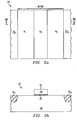
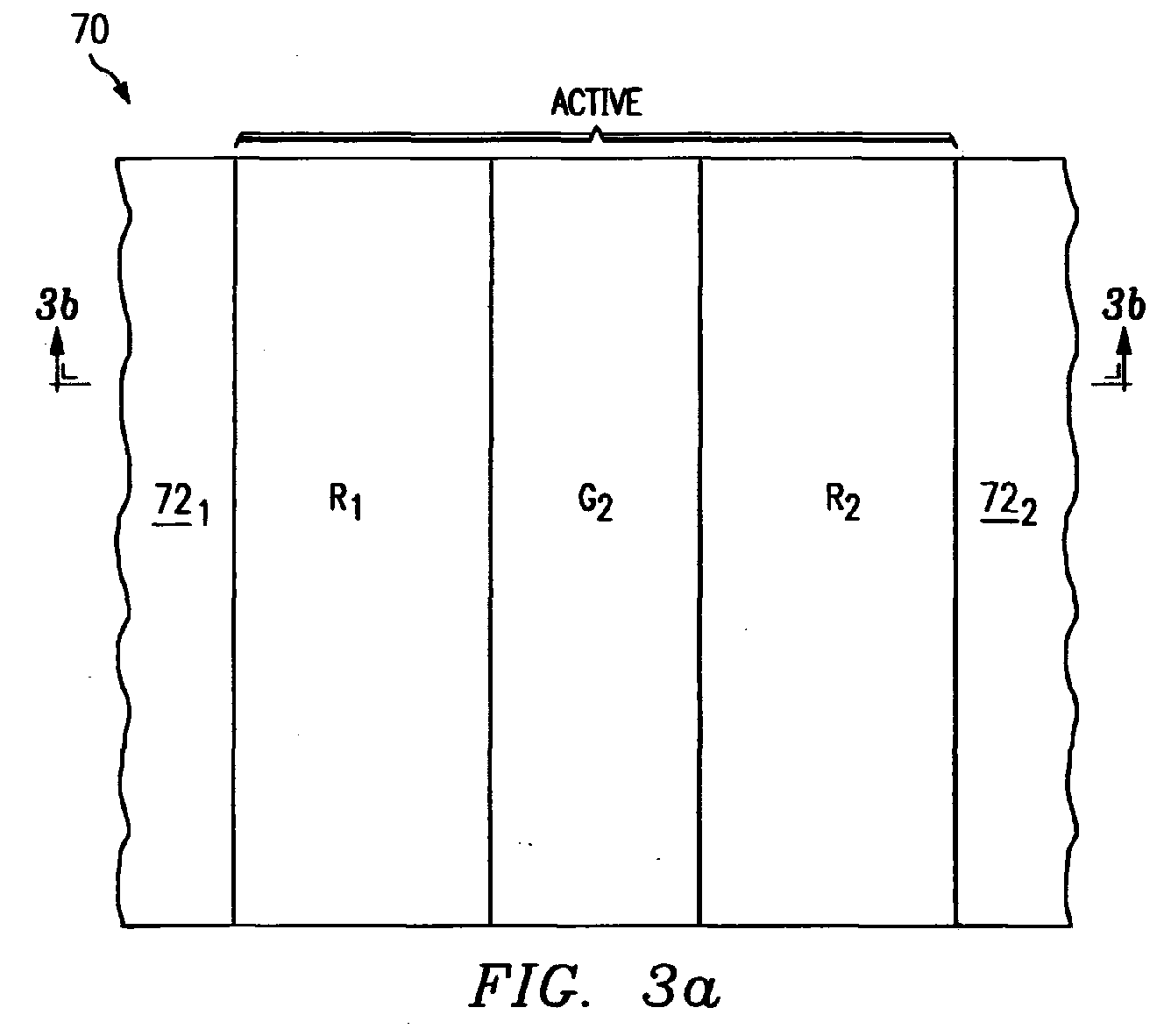
- Figure 3a illustrates a plan view, and Figure 3b a cross-sectional view, of a transistor 70 according to the preferred embodiment.
- transistor 70 is preferably implemented in I/O 60 of integrated circuit 40, but alternative implementations are also contemplated as within the inventive scope.
- transistor 70 is formed by defining an active semiconductor area between isolating regions 72 1 and 72 2 .
- Regions 72 1 and 72 2 may be shallow trench isolation ("STI") regions, yet alternate isolation techniques may be used (e.g., field oxide).
- STI shallow trench isolation
- the active region is provided by a semiconductor substrate 78.
- the active area may be provided by a well region (or more than one well region).
- a gate dielectric 74 is formed over the active area, and it may be an oxide, a thermally grown silicon dioxide, a nitride, an oxynitride, or a combination of these or other insulators.
- a gate conductor 76 is formed over gate dielectric 74, such as by forming a layer of material which is patterned and etched to form gate conductor 76. Gate conductor 76 is preferably polysilicon, although other materials may be used.
- gate conductor 76 is also shown by a schematic indication in Figures 3a and 3b with the identifier "G 2 .”
- the formation of gate G 2 generally separates the active region into two exposed regions R 1 and R 2 adjacent to respective sidewalls of gate G 2 and which, as demonstrated below, provide areas in which source/drain regions for the transistor are subsequently formed.
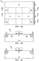
- Figures 4a through 4c illustrate selective formation of lightly-doped drain regions according to the preferred embodiment. More particularly, Figure 4a illustrates the plan view of transistor 70 after a mask M 1 is formed over the device, while Figures 4b and 4c illustrate cross-sectional views taken along lines 4b and 4c, respectively, in Figure 4a.
- mask M 1 may be formed using a standard photoresist process.
- mask M 1 is preferably shaped so that includes like-dimension elements, with each element spanning perpendicular to gate G 2 and completely across the active region of transistor 70, where each element preferably spans a same length, M 1 in the direction along gate G 2 .
- mask M 1 includes two such elements, but as explained below in actual implementation a much larger number of elements may be used. As a result of the various elements, mask M 1 covers only certain areas of the active region of transistor 70, thereby leaving other areas of that active region exposed. Once mask M 1 is in place, a dopant implant is performed so that lightly-doped regions are formed in the exposed active areas.
- the type of dopant may be selected by one skilled in the art according to the desired conductivity type of the transistor. Thus, for an NMOS transistor the dopant is an n-type dopant, whereas for a PMOS transistor the dopant is a p-type dopant.
- the implant creates two different portions for each source/drain of transistor 70, a first portion which includes the areas that receive the implant (because of a lack of an overlying mask element) and a second portion which includes the areas that do not directly receive the implant (because of an overlying mask element). As detailed below, these two portions therefore have different electrical resistance.
- Figure 4b illustrates a cross-sectional of view of transistor 70 along an area of active region that is in the first portion created by mask M 1 , that is, which is uncovered by mask M 1 and which for sake of reference is identified as view 70 1 . Since view 70 1 results from an exposed area, then lightly-doped regions 80 1 and 80 2 are formed within the active region, and in the present example they are self-aligned with respect to the sidewalls of gate conductor 76. Moreover, by the nature of the dopant implant, and possibly due to one or more subsequent annealing steps, the dopants diffuse laterally to a certain extent under gate conductor 76.
- Figure 4c illustrates a cross-sectional view of transistor 70 along an area of active region that is in the second portion created by mask M 1 , that is, which is covered by mask M 1 and which for sake of reference is identified as view 70 2 . Due to the coverage by mask M 1 in this area, then no lightly-doped regions are formed within the active region shown in Figure 4c. Given Figures 4b and 4c, one skilled in the art should appreciate how these same cross-sections may appear at other cross-sectional locations for transistor 70.
- lightly doped diffused regions may be formed to some extent in areas covered by mask M 1 . However, these lightly doped diffused regions will have a lesser dopant concentration as opposed to those areas of the active region which are completely exposed by virtue of the shape of mask M 1 .
- Figure 5 illustrates a simplified plot of the dopant concentration in the active region of transistor 70 and resulting from the implant using mask M 1 .
- the vertical plot axis depicts dopant concentration while the horizontal axis depicts the y-dimension shown in Figure 4a. From Figure 5, therefore, one skilled in the art will appreciate that dopant concentration is at its peak in areas exposed by the mask and then it falls off toward zero in the areas where mask M 1 is present. However, a drop all the way to zero will depend on the length of the dimension M 1.
- M 1 the greater the size of M 1 , the greater the chance that certain cross-sections taken perpendicular to gate G 2 may have little or no lightly doped diffused regions, with the latter being illustrated in Figure 4c.
- two aspects are endeavored to occur with mask M 1 .
- the dimension M 1 is reduced to as small as possible given the available technology (e.g., 0.2 micron under contemporary processes). Indeed, with such a reduced size, note that the number of mask elements may be much greater than two as shown in Figure 4a, as depending on the total length of the active area in the dimension along gate G 2 .
- the dimension M 1 is selected so that the exposed length between each portion of mask M 1 , shown as the dimension E 1 in Figure 4a, is the same as the dimension M 1 .
- a symmetry is maintained as between the masked areas and the unmasked (i.e., exposed) areas of the active area.
- the resulting structure of transistor 70 may be pictured to include numerous slices (taken in the dimension perpendicular to gate G 2 ), wherein the concentration of the lightly doped diffused region of each slice formed in an area underlying mask M 1 will differ only slightly from the immediately adjacent slice when examined in the direction along (i.e., parallel to) the gate conductor, thereby creating a gradient of dopant concentration in these slices.
- the masked slices will include to some extent a pair of lightly doped diffused regions as shown in Figure 4b, but the source/drain resistance for such slices will be greater than those slices which are formed in the active areas left exposed by mask M 1 .
- the dopant concentration in the unmasked areas will be greater than the zero or non-zero dopant concentration in the masked areas.
- the dopant concentration taken along the lightly doped diffused portion of that region will vary when examined in the direction along (i.e., parallel to) the gate conductor.
- a varying resistance occurs in the source/drain in the direction parallel to the gate conductor.
- Figures 6a and 6b illustrate cross-sectional views 70 1 and 70 2 from Figures 4b and 4c, respectively, after additional processing steps which occur once mask M 1 is removed.
- insulating sidewalls 84 1 and 84 2 are formed along the sidewalls of gate conductor 76, and these sidewalls are constructed according to techniques known in the art. For example, an insulating layer may be formed overlying transistor 70, and that layer is then etched to form insulating sidewalls 84 1 and 84 2 .
- a second dopant implant step is performed.
- doped regions 82 1 and 82 2 are formed within substrate 78, and they are self-aligned with respect to insulating sidewalls 84 1 and 84 2 , respectively.
- the combination of doped region 82 1 and lightly doped diffused region 80 1 forms the transistor source in view 70 1 and is schematically labeled S 2
- the combination of doped region 82 2 and lightly doped diffused region 80 2 forms the transistor drain in view 70 1 and is schematically labeled D 2
- regions 82 1 and 82 2 alone form source S 2 and drain D 2 , respectively.
- various additional components may be connected to or formed in connection with transistor 70 as may be ascertainable by one skilled in the art.
- transistor 70 is implemented as part of I/O 60.
- the same doping step used to create the varying lightly doped diffused regions in the transistors of I/O 60 is also used to form lightly doped diffused regions for transistors in core 50; however, for the core transistors they preferably are constructed using a standard lightly doped diffused region process without a mask that partially exposes their active regions (i.e., like mask M 1 ) and, thus, the core transistors include uniform doping concentration in their lightly doped diffused regions as depicted in Figure 1a.
- the transistors of I/O 60 have, as demonstrated in Figures 5 and 6a and 6b, a varying source/drain resistance due to the gradient of dopant concentration that occurs in the locations of lightly doped diffused regions, whereas the transistors of core 50 have a uniform or non-varying source/drain resistance due to the uniform doping concentrations in their lightly doped diffused regions.
- the lightly doped diffused region gradient of the former gives rise to a larger overall effective source/drain resistance as compared to the source/drain resistance of the latter.
- the transistors of I/O 60 are more resistant to ESD as compared to the transistors of core 50.
- the relatively greater source/drain resistance of the transistors of I/O 60 reduces the chance of runaway current occurring across a filament in those transistors during an ESD event.
- this increased resistance is achieved efficiently in that the same lightly doped diffused region step is used for both core 50 and I/O 60, that is, without adding a separate doping step for the relatively fewer number of transistors of I/O 60 compared to the larger number of transistors of core 50.
- the difference in the respective lightly doped diffused region resistance as between I/O 60 and core 50 is achieved by implementing a mask that selectively exposes the transistor active regions as depicted by mask M 1 .
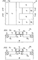
- Figures 7a through 7c illustrate an alternative embodiment of a transistor 90, again which is preferably implemented to form the transistors in I/O 60. More particularly, Figure 7a illustrates a plan view of transistor 90 after a mask M 2 is formed over the device, while Figures 7b and 7c illustrate cross-sectional views taken along line 7b and line 7c, respectively, in Figure 7a, and after a few additional processing steps.
- transistor 90 is comparable in many respects to transistor 70 described above and, thus, those common aspects are not detailed again having been discussed earlier. Looking therefore to the difference between transistor 70 and transistor 90, it arises in that mask M 2 is identical to mask M 1 (i.e., with selective openings) with respect to the drain of transistor 90, but mask M 2 does not cover the source of transistor 90.
- the source includes a lightly doped diffused region while the drain does not. More particularly, looking to Figure 7b, it illustrates a semiconductor substrate 98 with an active region defined between isolating regions 92 1 and 92 2 , and with a gate conductor 96 separated from substrate 98 by a gate dielectric 94.
- a first doping step occurs with mask M 2 in place and thereby forms lightly doped diffused region 100 1 as shown on the source side of transistor view 90 1 , but no symmetrical region is formed on the drain side of transistor view 90 1 because it is covered by mask M 2 .
- mask M 2 is removed, insulating sidewalls 104 1 and 104 2 are formed, and a second doping step is performed to create doped regions 102 1 and 102 2 . Consequently, source S 3 of transistor view 90 1 includes both doped region 102 1 as well as lightly doped diffused region 100 1 , while drain D 3 of transistor view 90 1 includes only a doped region 102 2 .
- both the source and drain include a lightly doped diffused region. More particularly, looking to Figure 7c, it illustrates that once gate conductor 96 is formed, the first doping step in connection with mask M 2 forms lightly doped diffused regions 100 1 and 100 2 which are self-aligned to opposite sidewalls of gate conductor 96.
- the second doping step creates doped regions 102 1 and 102 2 , but in view 90 2 each of those regions combines with a respective lightly doped diffused region 100 1 and 100 2 , thereby providing source S 3 and drain D 3 , respectively.
- a source may be connected to a fixed potential whereas the drain is connected to a switching potential.
- the current capacity of the transistor is much more limited if the source potential is increased as opposed to increasing the drain potential. Accordingly, to avoid increasing the source potential, transistor 90 may be used in such implementations whereby the effective drain resistance is increased due to the selective openings of mask M 2 over part of the active region in which the drain is formed, whereas the source resistance (and, hence, source potential) is unaffected by mask M 2 because it does not cover the active region in which the source is formed.
Landscapes
- Insulated Gate Type Field-Effect Transistor (AREA)
- Metal-Oxide And Bipolar Metal-Oxide Semiconductor Integrated Circuits (AREA)
- Semiconductor Integrated Circuits (AREA)
Abstract
Description
Claims (31)
- A method of forming a transistor in a semiconductor active area, which method comprising:forming a gate structure in a fixed relationship to the semiconductor active area and comprising a first sidewall and a second sidewall and thereby defining a first source/drain region adjacent the first sidewall and a second source/drain region adjacent the second sidewall; andforming a lightly doped diffused region in the first source/drain region and extending under the gate structure, said lightly doped diffused region having a varying resistance in a direction parallel to the gate structure.
- The method of claim 1, wherein the step of forming a lightly doped diffused region comprises:selectively masking the first source/drain region such that a portion of the first source/drain region is covered and a portion of the first source/drain region is exposed; andduring the selectively masking step, directing dopants toward the first source/drain region.
- The method of claim 2, wherein said directing step causes a first concentration of dopants to be implanted in the portion of the first source/drain region that is exposed while a different concentration of dopants are implanted in the portion of the first source/drain region that is covered, the first concentration being greater than the different concentration.
- The method of claim 2, wherein the step of selectively masking comprises:wherein the mask comprises a plurality of elements such that the portion of the first source/drain region that is covered is covered by the plurality of elements and such that the portion of the first source/drain region that is exposed is not covered by the plurality of elements.performing a first selectively masking step using a mask; and
- The method of claim 4, wherein each element of the plurality of elements spans in a direction perpendicular to the gate structure and has a same first distance length in a direction along the gate structure.
- The method of claim 5, wherein each element of the plurality of elements has a same second distance length, along the gate structure, between itself and an adjacent other one of the plurality of elements.
- The method of claim 6, wherein the first same distance length equals the same second distance length.
- The method of claim 2, wherein the transistor is formed as part of an integrated circuit comprising input/output circuitry and core circuitry; and
wherein the transistor is formed as part of the input/output circuitry. - The method of claim 8, wherein the transistor comprises a first transistor in a first plurality of transistors;
wherein the step of selectively masking selectively masks a respective first source/drain for each transistor in the first plurality of transistors; and
wherein the step of directing dopants directs dopants toward a respective first source/drain for each transistor in the first plurality of transistors. - The method of claim 9, wherein each transistor of the first plurality of transistors is formed as part of the input/output circuitry.
- The method of claim 8, wherein the transistor comprises a first transistor, and wherein the method further further comprisises:forming a second transistor in the core circuitry, wherein the step of directing dopants further directs dopants into a first source/drain and a second source/drain of the second transistor.
- The method of claim 11, wherein the step of selectively masking comprises selectively masking using a mask; and
wherein the active area of the second transistor is not masked by the mask. - The method of claim 2, wherein the step of directing dopants comprises directing n-type dopants.
- The method of claim 2, wherein the step of directing dopants comprises directing p-type dopants.
- The method of claim 2, wherein the step of selectively masking comprises selectively masking using a mask; and
wherein the second source/drain is not masked by the mask. - The method of claim 2, wherein the step of selectively masking comprises a first selectively masking step performed using a mask;
and further comprising, at the same time as the first selectively masking step, the step of using the mask for second selectively masking the second source/drain region such that a portion of the second source/drain region is covered and a portion of the second source/drain region is exposed;
and wherein the step of directing dopants further comprises directing dopants toward the second source/drain region. - The method of claim 16, wherein as a result of the directing step a first concentration of dopants are implanted in the portion of the first source/drain region that is exposed and the second source/drain that is exposed while a different concentration of dopants are implanted in the portion of the first source/drain region that is covered and the portion of the second source/drain region that is covered, wherein the first concentration is greater than the different concentration.
- The method of claim 17, wherein the step of selectively masking comprises a first selectively masking step performed using a mask; and
wherein the mask comprises a plurality of elements such that the portion of the first source/drain region that is covered and the portion of the second source/drain region that is covered are covered by the plurality of elements and such that the portion of the first source/drain region that is exposed and the portion of the second source/drain region that is exposed are not covered by the plurality of elements. - The method of claim 18, wherein each element of the plurality of elements spans in a direction perpendicular to the gate structure and has a same first distance length in a direction along the gate structure.
- The method of claim 19, wherein each element of the plurality of elements has a same second distance length, along the gate structure, between itself and an adjacent other one of the plurality of elements.
- The method of claim 20, wherein the first same distance length equals the same second distance length.
- The method of claim 17, wherein the transistor is formed as part of an integrated circuit comprising input/output circuitry and core circuitry; and
wherein the transistor is formed as part of the input/output circuitry. - The method of claim 22, wherein the transistor comprises a first transistor in a first plurality of transistors;
wherein the step of selectively masking selectively masks a respective first source/drain and a respective second source/drain for each transistor in the first plurality of transistors; and
wherein the step of directing dopants directs dopants toward a respective first source/drain for each transistor in the first plurality of transistors and a respective second source/drain for each transistor in the first plurality of transistors. - The method of claim 17, wherein the step of directing dopants comprises directing n-type dopants.
- The method of claim 17, wherein the step of directing dopants comprises directing p-type dopants.
- An integrated circuit comprising a transistor, which transistor comprising:a gate structure in a fixed relationship to a semiconductor active area and comprising a first sidewall and a second sidewall and thereby defining a first source/drain region adjacent the first sidewall and a second source/drain region adjacent the second sidewall; anda lightly doped diffused region formed in the first source/drain region and extending under the gate structure, wherein the lightly doped diffused region comprises a varying resistance in a direction parallel to the gate structure.
- The integrated circuit of claim 26, wherein the integrated circuit further comprises input/output circuitry and core circuitry; and
wherein the transistor is formed as part of the input/output circuitry. - The integrated circuit of claim 26, wherein the integrated circuit further comprises a first plurality of transistors;
wherein the transistor comprises a first transistor in the first plurality of transistors;
wherein each transistor of the plurality of transistors comprises:a gate structure in a fixed relationship to a semiconductor active area and comprising a first sidewall and a second sidewall and thereby defining a first source/drain region adjacent the first sidewall and a second source/drain region adjacent the second sidewall; anda lightly doped diffused region formed in the first source/drain region and extending under the gate structure, wherein the lightly doped diffused region comprises a varying resistance in a direction parallel to the gate structure. - The integrated circuit of claim 28, wherein the integrated circuit further comprises input/output circuitry and core circuitry; and
wherein the plurality of transistors are formed as part of the input/output circuitry. - The integrated circuit of claim 28, wherein each transistor of the plurality of transistors further comprises a lightly doped diffused region formed in the second source/drain region and extending under the gate structure, wherein the lightly doped diffused region formed in the second source/drain region comprises a varying resistance in a direction parallel to the gate structure.
- The integrated circuit of claim 28, wherein the integrated circuit further comprises input/output circuitry and core circuitry; and
wherein the plurality of transistors are formed as part of the input/output circuitry.
Applications Claiming Priority (2)
| Application Number | Priority Date | Filing Date | Title |
|---|---|---|---|
| US257489 | 1988-10-13 | ||
| US25748900P | 2000-12-21 | 2000-12-21 |
Publications (3)
| Publication Number | Publication Date |
|---|---|
| EP1217661A2 true EP1217661A2 (en) | 2002-06-26 |
| EP1217661A3 EP1217661A3 (en) | 2006-10-18 |
| EP1217661B1 EP1217661B1 (en) | 2016-07-27 |
Family
ID=22976509
Family Applications (1)
| Application Number | Title | Priority Date | Filing Date |
|---|---|---|---|
| EP01000777.1A Expired - Lifetime EP1217661B1 (en) | 2000-12-21 | 2001-12-20 | Transistor circuit with varying resistance lightly doped diffused regions for electrostatic discharge (ESD) protection |
Country Status (3)
| Country | Link |
|---|---|
| US (1) | US6730582B2 (en) |
| EP (1) | EP1217661B1 (en) |
| JP (1) | JP2002231729A (en) |
Cited By (1)
| Publication number | Priority date | Publication date | Assignee | Title |
|---|---|---|---|---|
| EP1956868A2 (en) | 2007-02-09 | 2008-08-13 | Vestel Elektronik Sanayi ve Ticaret A.S. | Method for determining the angular position of a sound source |
Families Citing this family (1)
| Publication number | Priority date | Publication date | Assignee | Title |
|---|---|---|---|---|
| KR100734670B1 (en) * | 2005-12-26 | 2007-07-02 | 동부일렉트로닉스 주식회사 | Method of manufacturing semiconductor device |
Family Cites Families (13)
| Publication number | Priority date | Publication date | Assignee | Title |
|---|---|---|---|---|
| US5019888A (en) | 1987-07-23 | 1991-05-28 | Texas Instruments Incorporated | Circuit to improve electrostatic discharge protection |
| US5238859A (en) * | 1988-04-26 | 1993-08-24 | Kabushiki Kaisha Toshiba | Method of manufacturing semiconductor device |
| US5246872A (en) * | 1991-01-30 | 1993-09-21 | National Semiconductor Corporation | Electrostatic discharge protection device and a method for simultaneously forming MOS devices with both lightly doped and non lightly doped source and drain regions |
| JP3199808B2 (en) * | 1991-05-14 | 2001-08-20 | セイコーインスツルメンツ株式会社 | Semiconductor integrated circuit device |
| US5675168A (en) * | 1994-04-01 | 1997-10-07 | Matsushita Electric Industrial Co., Ltd. | Unsymmetrical MOS device having a gate insulator area offset from the source and drain areas, and ESD protection circuit including such a MOS device |
| JP3008154B2 (en) * | 1994-12-19 | 2000-02-14 | セイコーインスツルメンツ株式会社 | Method for manufacturing semiconductor device |
| US5508212A (en) * | 1995-04-27 | 1996-04-16 | Taiwan Semiconductor Manufacturing Co. | Salicide process for a MOS semiconductor device using nitrogen implant of titanium |
| US5721439A (en) * | 1996-04-10 | 1998-02-24 | Winbond Electronics Corporation | MOS transistor structure for electro-static discharge protection circuitry |
| US5763919A (en) * | 1996-07-08 | 1998-06-09 | Winbond Electronics Corporation | MOS transistor structure for electro-static discharge protection circuitry having dispersed parallel paths |
| JPH10321842A (en) * | 1997-05-15 | 1998-12-04 | Toshiba Microelectron Corp | Semiconductor device |
| US6013570A (en) * | 1998-07-17 | 2000-01-11 | Advanced Micro Devices, Inc. | LDD transistor using novel gate trim technique |
| US6153913A (en) * | 1999-06-30 | 2000-11-28 | United Microelectronics Corp. | Electrostatic discharge protection circuit |
| US6215156B1 (en) * | 1999-08-02 | 2001-04-10 | Taiwan Semiconductor Manufacturing Corporation | Electrostatic discharge protection device with resistive drain structure |
-
2001
- 2001-12-14 US US10/020,687 patent/US6730582B2/en not_active Expired - Lifetime
- 2001-12-20 JP JP2001387479A patent/JP2002231729A/en active Pending
- 2001-12-20 EP EP01000777.1A patent/EP1217661B1/en not_active Expired - Lifetime
Cited By (1)
| Publication number | Priority date | Publication date | Assignee | Title |
|---|---|---|---|---|
| EP1956868A2 (en) | 2007-02-09 | 2008-08-13 | Vestel Elektronik Sanayi ve Ticaret A.S. | Method for determining the angular position of a sound source |
Also Published As
| Publication number | Publication date |
|---|---|
| US6730582B2 (en) | 2004-05-04 |
| EP1217661B1 (en) | 2016-07-27 |
| JP2002231729A (en) | 2002-08-16 |
| US20020079546A1 (en) | 2002-06-27 |
| EP1217661A3 (en) | 2006-10-18 |
Similar Documents
| Publication | Publication Date | Title |
|---|---|---|
| US6137144A (en) | On-chip ESD protection in dual voltage CMOS | |
| US6548874B1 (en) | Higher voltage transistors for sub micron CMOS processes | |
| US7214591B2 (en) | Method of fabricating high-voltage MOS device | |
| US6198131B1 (en) | High-voltage metal-oxide semiconductor | |
| EP1191577A1 (en) | MOSFET transistor | |
| KR100204986B1 (en) | Integrated circuit and manufacturing thereof | |
| JP2006510206A (en) | Integrated circuit structure | |
| US6274914B1 (en) | CMOS integrated circuits including source/drain plug | |
| EP0676798A2 (en) | Insulated gate field effect transistor with assymetric channel and method for fabricating | |
| JPH05251555A (en) | Manufacture of mos integrated circuit | |
| KR20010051913A (en) | Semiconductor apparatus and method of manufacture | |
| US20030127694A1 (en) | Higher voltage transistors for sub micron CMOS processes | |
| US6157062A (en) | Integrating dual supply voltage by removing the drain extender implant from the high voltage device | |
| US6040222A (en) | Method for fabricating an electrostatistic discharge protection device to protect an integrated circuit | |
| US6303420B1 (en) | Integrated bipolar junction transistor for mixed signal circuits | |
| US5675168A (en) | Unsymmetrical MOS device having a gate insulator area offset from the source and drain areas, and ESD protection circuit including such a MOS device | |
| US7138313B2 (en) | Method for creating a self-aligned SOI diode by removing a polysilicon gate during processing | |
| US6692998B2 (en) | Integrated high quality diode | |
| US20020164846A1 (en) | Integrated circuit devices with high and low voltage components and processes for manufacturing these devices | |
| US20120161235A1 (en) | Electrostatic discharge protection device and manufacturing method thereof | |
| US6831337B2 (en) | Transistor circuit with varying resistance lightly doped diffused regions for electrostatic discharge (“ESD”) protection | |
| US6730582B2 (en) | Transistor circuit with varying resistance lightly doped diffused regions for electrostatic discharge (ESD) protection | |
| KR100707900B1 (en) | Method of manufacturing semiconductor device | |
| US6130133A (en) | Fabricating method of high-voltage device | |
| US6514807B1 (en) | Method for fabricating semiconductor device applied system on chip |
Legal Events
| Date | Code | Title | Description |
|---|---|---|---|
| PUAI | Public reference made under article 153(3) epc to a published international application that has entered the european phase |
Free format text: ORIGINAL CODE: 0009012 |
|
| AK | Designated contracting states |
Kind code of ref document: A2 Designated state(s): AT BE CH CY DE DK ES FI FR GB GR IE IT LI LU MC NL PT SE TR |
|
| AX | Request for extension of the european patent |
Free format text: AL;LT;LV;MK;RO;SI |
|
| PUAL | Search report despatched |
Free format text: ORIGINAL CODE: 0009013 |
|
| AK | Designated contracting states |
Kind code of ref document: A3 Designated state(s): AT BE CH CY DE DK ES FI FR GB GR IE IT LI LU MC NL PT SE TR |
|
| AX | Request for extension of the european patent |
Extension state: AL LT LV MK RO SI |
|
| 17P | Request for examination filed |
Effective date: 20070418 |
|
| AKX | Designation fees paid |
Designated state(s): DE FR GB |
|
| 17Q | First examination report despatched |
Effective date: 20070615 |
|
| REG | Reference to a national code |
Ref country code: DE Ref legal event code: R079 Ref document number: 60150022 Country of ref document: DE Free format text: PREVIOUS MAIN CLASS: H01L0027020000 Ipc: H01L0029660000 |
|
| GRAP | Despatch of communication of intention to grant a patent |
Free format text: ORIGINAL CODE: EPIDOSNIGR1 |
|
| RIC1 | Information provided on ipc code assigned before grant |
Ipc: H01L 27/02 20060101ALI20160119BHEP Ipc: H01L 29/06 20060101ALI20160119BHEP Ipc: H01L 29/78 20060101ALI20160119BHEP Ipc: H01L 29/66 20060101AFI20160119BHEP |
|
| INTG | Intention to grant announced |
Effective date: 20160208 |
|
| GRAS | Grant fee paid |
Free format text: ORIGINAL CODE: EPIDOSNIGR3 |
|
| GRAA | (expected) grant |
Free format text: ORIGINAL CODE: 0009210 |
|
| AK | Designated contracting states |
Kind code of ref document: B1 Designated state(s): DE FR GB |
|
| REG | Reference to a national code |
Ref country code: GB Ref legal event code: FG4D |
|
| REG | Reference to a national code |
Ref country code: DE Ref legal event code: R096 Ref document number: 60150022 Country of ref document: DE |
|
| REG | Reference to a national code |
Ref country code: FR Ref legal event code: PLFP Year of fee payment: 16 |
|
| PGFP | Annual fee paid to national office [announced via postgrant information from national office to epo] |
Ref country code: GB Payment date: 20161125 Year of fee payment: 16 Ref country code: FR Payment date: 20161117 Year of fee payment: 16 |
|
| PGFP | Annual fee paid to national office [announced via postgrant information from national office to epo] |
Ref country code: DE Payment date: 20161220 Year of fee payment: 16 |
|
| REG | Reference to a national code |
Ref country code: DE Ref legal event code: R097 Ref document number: 60150022 Country of ref document: DE |
|
| PLBE | No opposition filed within time limit |
Free format text: ORIGINAL CODE: 0009261 |
|
| STAA | Information on the status of an ep patent application or granted ep patent |
Free format text: STATUS: NO OPPOSITION FILED WITHIN TIME LIMIT |
|
| 26N | No opposition filed |
Effective date: 20170502 |
|
| REG | Reference to a national code |
Ref country code: DE Ref legal event code: R119 Ref document number: 60150022 Country of ref document: DE |
|
| GBPC | Gb: european patent ceased through non-payment of renewal fee |
Effective date: 20171220 |
|
| REG | Reference to a national code |
Ref country code: FR Ref legal event code: ST Effective date: 20180831 |
|
| PG25 | Lapsed in a contracting state [announced via postgrant information from national office to epo] |
Ref country code: DE Free format text: LAPSE BECAUSE OF NON-PAYMENT OF DUE FEES Effective date: 20180703 Ref country code: FR Free format text: LAPSE BECAUSE OF NON-PAYMENT OF DUE FEES Effective date: 20180102 |
|
| PG25 | Lapsed in a contracting state [announced via postgrant information from national office to epo] |
Ref country code: GB Free format text: LAPSE BECAUSE OF NON-PAYMENT OF DUE FEES Effective date: 20171220 |