EP1217652A1 - A method for controlling interfacial oxide at a polycrystalline/monocrystalline silicon interface - Google Patents
A method for controlling interfacial oxide at a polycrystalline/monocrystalline silicon interface Download PDFInfo
- Publication number
- EP1217652A1 EP1217652A1 EP00830834A EP00830834A EP1217652A1 EP 1217652 A1 EP1217652 A1 EP 1217652A1 EP 00830834 A EP00830834 A EP 00830834A EP 00830834 A EP00830834 A EP 00830834A EP 1217652 A1 EP1217652 A1 EP 1217652A1
- Authority
- EP
- European Patent Office
- Prior art keywords
- monocrystalline silicon
- vacuum
- comprised
- temperature
- treatment
- Prior art date
- Legal status (The legal status is an assumption and is not a legal conclusion. Google has not performed a legal analysis and makes no representation as to the accuracy of the status listed.)
- Granted
Links
Images



Classifications
-
- H—ELECTRICITY
- H10—SEMICONDUCTOR DEVICES; ELECTRIC SOLID-STATE DEVICES NOT OTHERWISE PROVIDED FOR
- H10D—INORGANIC ELECTRIC SEMICONDUCTOR DEVICES
- H10D10/00—Bipolar junction transistors [BJT]
- H10D10/01—Manufacture or treatment
- H10D10/051—Manufacture or treatment of vertical BJTs
-
- H—ELECTRICITY
- H10—SEMICONDUCTOR DEVICES; ELECTRIC SOLID-STATE DEVICES NOT OTHERWISE PROVIDED FOR
- H10D—INORGANIC ELECTRIC SEMICONDUCTOR DEVICES
- H10D10/00—Bipolar junction transistors [BJT]
- H10D10/231—Tunnel BJTs
-
- H—ELECTRICITY
- H10—SEMICONDUCTOR DEVICES; ELECTRIC SOLID-STATE DEVICES NOT OTHERWISE PROVIDED FOR
- H10P—GENERIC PROCESSES OR APPARATUS FOR THE MANUFACTURE OR TREATMENT OF DEVICES COVERED BY CLASS H10
- H10P32/00—Diffusion of dopants within, into or out of wafers, substrates or parts of devices
- H10P32/10—Diffusion of dopants within, into or out of semiconductor bodies or layers
- H10P32/14—Diffusion of dopants within, into or out of semiconductor bodies or layers within a single semiconductor body or layer in a solid phase; between different semiconductor bodies or layers, both in a solid phase
- H10P32/1408—Diffusion of dopants within, into or out of semiconductor bodies or layers within a single semiconductor body or layer in a solid phase; between different semiconductor bodies or layers, both in a solid phase from or through or into an external applied layer, e.g. photoresist or nitride layers
- H10P32/141—Diffusion of dopants within, into or out of semiconductor bodies or layers within a single semiconductor body or layer in a solid phase; between different semiconductor bodies or layers, both in a solid phase from or through or into an external applied layer, e.g. photoresist or nitride layers the applied layer comprising oxides only
- H10P32/1412—Diffusion of dopants within, into or out of semiconductor bodies or layers within a single semiconductor body or layer in a solid phase; between different semiconductor bodies or layers, both in a solid phase from or through or into an external applied layer, e.g. photoresist or nitride layers the applied layer comprising oxides only through the applied layer
-
- H—ELECTRICITY
- H10—SEMICONDUCTOR DEVICES; ELECTRIC SOLID-STATE DEVICES NOT OTHERWISE PROVIDED FOR
- H10P—GENERIC PROCESSES OR APPARATUS FOR THE MANUFACTURE OR TREATMENT OF DEVICES COVERED BY CLASS H10
- H10P32/00—Diffusion of dopants within, into or out of wafers, substrates or parts of devices
- H10P32/10—Diffusion of dopants within, into or out of semiconductor bodies or layers
- H10P32/17—Diffusion of dopants within, into or out of semiconductor bodies or layers characterised by the semiconductor material
- H10P32/171—Diffusion of dopants within, into or out of semiconductor bodies or layers characterised by the semiconductor material being group IV material
Definitions
- the present invention relates to fabrication techniques of integrated semiconductor devices and in particular to fabrication techniques of poly-emitter bipolar devices.
- Bipolar devices with emitter of doped polycrystalline silicon commonly referred to as poly-emitter bipolar devices, typically bipolar transistors
- poly-emitter bipolar devices are very numerous in many integrated circuits designed for operating at radio frequency because they permit the making of exceptionally shallow emitter junctions and of self aligned structures with modem fabrication techniques.
- poly-emitter bipolar transistors provide for a higher switching speed and a higher current gain (HFE), in common emitter configuration, substantially without increasing the base resistance, than their counterparts with a classical structure.
- HFE current gain
- FIG. 1 Distribution diagrams of holes in a poly-emitter device are depicted in Fig. 1, while the holes distribution in the polysilicon layer is depicted in Fig. 2.
- both the emitter resistance (R E ) as well as the current gain (HFE) depend strongly by the barrier characteristics of the oxide film at the interface.
- R E and HFE are proportional to the expression: e A ⁇ Bx wherein ⁇ and ⁇ represent respectively the thickness and the highness of the barrier and A and B are constants.
- ⁇ is about 0.6 eV for electrons and 1.1 eV for holes, but, in the case of the oxide that is presumed to be present at the interface between the monocrystalline silicon and the polysilicon upon detecting a certain amount of oxygen, per unit area these values appear to be markedly depressed because of the non stoichiometric form of such an interface oxide.
- the trade-off between the R E and HFE values depends on the barrier property of the interface film of oxidized silicon though the HFE shows an increasingly marked increase upon an increase of the amount or "thickness" of the interface oxide (or more precisely of the concentration of oxygen atoms per unit area) .
- the main technical problem in fabricating this kind of integrated structures is represented by the difficulty of controlling the physical-chemical characteristics of the interface, in consideration of the commonly used techniques for depositing the polysilicon that typically are based on a low pressure chemical vapor deposition process (LPCVD).
- LPCVD low pressure chemical vapor deposition process
- the fabrication processes may contemplate a treatment of the surface of the monocrystalline silicon in the emitter area with a diluted solution of hydrofluoric acid (commonly 1% by weight) before introducing the wafer in the polysilicon LPCVD reactor.
- Hydrogen passivation of the silicon surface by contacting it with hydrofluoric acid is effective in limiting a spontaneous re-oxidation of the silicon surface exposed to air at room temperature.
- the monocrystalline silicon surface oxidizes freely determining a wide dispersion of the values of the current gain of the transistors so fabricated.
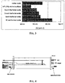
- FIG. 4 A typical LPCVD reactor is depicted in Fig. 4.
- a typical LPCVD process for depositing a layer of polysilicon is illustrated in a general manner in the following table, though conditions of each of the 14 phases may be slightly different, depending on the type of device being integrated and on the fabrication technology.
- inert gas such as nitrogen (N 2 ), helium or argon
- the pre-oxidation treatment with H 2 O 2 requires sophisticated control devices because of the remarkable reactivity of silicon even at low temperature [2] .
- a residual hydrogen passivation of the surface of the monocrystalline silicon may be still found up to a temperature of about 300°C, it has been demonstrated that silicon begins to oxidize well before hydrogen passivation of its surface has completely disappeared.
- a thermal oxidation pre-treatment in presence of oxygen and/or steam of the monocrystalline silicon surface to prevent an uncontrolled oxidation during loading, heating and evacuating of the chamber of the LPCVD reactor of polysilicon deposition is not practicable because of the too fast kinetic of the thermal oxidation process that makes a precise control, for the extremely small amount of it that is required, almost impossible or at least extremely difficult.
- the presence of an oxidizing atmosphere inside the LPCVD reactor itself would be hardly compatible with the silicon precursor compounds (SiH 4 ) from the point of safety.
- the process of the present invention solves excellently the above mentioned problems of controlling the quantity and uniformity of distribution of bonded oxygen atoms at the interface between the polysilicon and the monocrystalline silicon by carrying out, after having loaded the wafer inside the heated chamber of the reactorand evacuated the chamber of the LPCVD reactor under nitrogen atmosphere, a treatment of the wafer with hydrogen at a temperature generally comprised between 500 and 1200°C and at a vacuum generally comprised between 0.1 Pa and 60000 Pa, and preferably at a temperature of 850°C ⁇ 15°C and at a vacuum of 11000 Pa ⁇ 2000 Pa, for a time generally comprised between 0.1 and 120 minutes, and most preferably between 0.5 and 1.5 minutes.
- This treatment effectively removes substantially any and all the oxygen that may have combined with the silicon on the surface of the monocrystalline silicon during the loading inside the heated chamber of the reactor even if it is done under a nitrogen flux.
- Another treatment is carried out substantially under the same vacuum conditions and at a temperature generally comprised between 700 and 1000°C with nitrogen protoxide (N 2 O) for a time generally comprised between 0.1 and 120 minutes, preferably between 0.5 and 1.5 minutes.
- N 2 O nitrogen protoxide
- the gist of the invention is to pre-oxidize the silicon in a N 2 O atmosphere instead of using hydrogen peroxide according to prior art.
- N 2 O nitrogen protoxide
- NO toxic nitrogen oxide
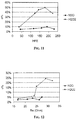
- the reduced oxidation kinetic of the process of the invention has effects that may be best appreciated from the diagram of Fig. 6.
- the transistors made according to the method of the invention have highly reproducible HFE values.
Landscapes
- Formation Of Insulating Films (AREA)
- Bipolar Transistors (AREA)
Abstract
Description
| BOAT IN | BOAT=60 | 35 cm/min | |
| T=620°C | BOAT=5 | 25 cm/min | |
| BOAT IN | 5 cm/min | ||
| H1-N2=ON | |||
| T1 | t=3 min | ||
| PRE-VACUUM | H GATE=ON | ||
| T2 | t=4 min | ||
| VACUUM | GATE V=ON | ||
| T3 | t=4 min | ||
| LEAK-CHECK | GATE V=OFF | ||
| T4 | t=30 s | ||
| VACUUM | GATE V=ON | ||
| T5 | t=30 min | ||
| TEMP- | Low N2=200 sccm (flux measure) | ||
| CONTROL: TC SPIKE | N2 dil=200scm | ||
| T6 | t=30 min | ||
| TEMP- | Low N2=200 seem | ||
| CONTROL: TC SPIKE | N2 dil=200 scm | ||
| T7 | t=4 s | ||
| PRE-DEP | SiH4 US=OFF | ||
| SiH4 D=36 sccm | |||
| SiH4 I=44 seem | |||
| N2 dil=200 scm | |||
| T8 | t=40 min | ||
| DEPOSITION | SiH4 US=ON | ||
| SiH4 D=36 sccm | |||
| SiH4 I=44 sccm | |||
| N2 dil=200 scm | |||
| T9 | t=100 s | ||
| POST DEP | SiH4 US=OFF | ||
| SiH4 D=0 seem | |||
| SiH4 I=0 seem | |||
| N2 dil=200 scm | |||
| T10 | t=5 min | ||
| PURGE | Low N2=200 seem | ||
| N2 dil=250scm | |||
| HOLD | MANUAL START | ||
| Low N2=200 sccm | |||
| N2 dil=250scm | |||
| T11 | t=13 min | ||
| VENT | N2=5 slm | ||
| BOAT OUT | H1-N2=ON | ||
| BOAT=25 cm/min |
Claims (4)
- A process for controlling the amount and the uniformity of distribution of oxygen atoms at the interface between an emitter region of the surface of a monocrystalline silicon wafer and a layer of polysilicon deposited thereon by a low pressure chemical vapor deposition technique, comprising the steps of cleaning and passivating said surface of the monocrystalline silicon by contacting it with a solution of hydrofluoric acid, rinsing and drying the wafer, loading the wafer inside a reactor for chemical vapor deposition, evacuating the reactor at a vacuum comprised between 0.1 Pa and 15000 Pa, raising the temperature inside the reactor and depositing said polysilicon, characterized in that it comprises the steps ofkeeping an atmosphere of a gas belonging to the group composed of nitrogen, argon and helium in the reactor during said evacuating and heating phases;passivating the silicon surface with hydrogen at a vacuum comprised between 0.1 Pa and 60000 Pa and at a temperature comprised between 500 and 1200°C, for a time comprised between 0.1 and 120 minutes;exposing the passivated silicon surface to an atmosphere of nitrogen protoxide (N2O) for a time comprised between 0.1 and 120 minutes at a vacuum comprised between 0.1 Pa and 60000 Pa and at a temperature comprised between 700 and 1000°C;lowering the temperature inside the reactor until reaching a value comprised between 500°C and 800°C before starting the deposition of polysilicon.
- The process of claim 1, characterized in that said treatment with nitrogen protoxide (N2O) is carried out under a vacuum of 11000 Pa and at a temperature of 850°C.
- The process of claim 1, wherein said solution of hydrofluoric acid is a 1% by weight aqueous solution of hydrofluoric acid.
- A process for fabricating semiconductor integrated devices comprising poly-emitter silicon transistors, characterized in that the formation of a polysilicon layer onto the emitter area of a monocrystalline silicon wafer of said bipolar transistors is carried out with a process as defined in claim 1.
Priority Applications (3)
| Application Number | Priority Date | Filing Date | Title |
|---|---|---|---|
| DE60005541T DE60005541T2 (en) | 2000-12-20 | 2000-12-20 | Process for the control of intermediate oxide in a monocrystalline / polycrystalline silicon intermediate layer |
| EP00830834A EP1217652B1 (en) | 2000-12-20 | 2000-12-20 | A method for controlling interfacial oxide at a polycrystalline/monocrystalline silicon interface |
| US10/032,334 US6642121B2 (en) | 2000-12-20 | 2001-12-18 | Control of amount and uniformity of oxidation at the interface of an emitter region of a monocrystalline silicon wafer and a polysilicon layer formed by chemical vapor deposition |
Applications Claiming Priority (1)
| Application Number | Priority Date | Filing Date | Title |
|---|---|---|---|
| EP00830834A EP1217652B1 (en) | 2000-12-20 | 2000-12-20 | A method for controlling interfacial oxide at a polycrystalline/monocrystalline silicon interface |
Publications (2)
| Publication Number | Publication Date |
|---|---|
| EP1217652A1 true EP1217652A1 (en) | 2002-06-26 |
| EP1217652B1 EP1217652B1 (en) | 2003-09-24 |
Family
ID=8175596
Family Applications (1)
| Application Number | Title | Priority Date | Filing Date |
|---|---|---|---|
| EP00830834A Expired - Lifetime EP1217652B1 (en) | 2000-12-20 | 2000-12-20 | A method for controlling interfacial oxide at a polycrystalline/monocrystalline silicon interface |
Country Status (3)
| Country | Link |
|---|---|
| US (1) | US6642121B2 (en) |
| EP (1) | EP1217652B1 (en) |
| DE (1) | DE60005541T2 (en) |
Families Citing this family (4)
| Publication number | Priority date | Publication date | Assignee | Title |
|---|---|---|---|---|
| US6734453B2 (en) | 2000-08-08 | 2004-05-11 | Translucent Photonics, Inc. | Devices with optical gain in silicon |
| US6949424B2 (en) * | 2003-08-28 | 2005-09-27 | Texas Instruments Incorporated | Single poly-emitter PNP using DWELL diffusion in a BiCMOS technology |
| JP4884180B2 (en) * | 2006-11-21 | 2012-02-29 | 東京エレクトロン株式会社 | Substrate processing apparatus and substrate processing method |
| CN109661554B (en) | 2016-08-08 | 2021-05-11 | 提克纳有限责任公司 | Thermally conductive polymer composition for heat sink |
Citations (2)
| Publication number | Priority date | Publication date | Assignee | Title |
|---|---|---|---|---|
| JPS58168275A (en) * | 1982-03-29 | 1983-10-04 | Fujitsu Ltd | Semiconductor device |
| EP0519854A2 (en) * | 1991-06-05 | 1992-12-23 | International Business Machines Corporation | A method for controlling interfacial oxide at a polycrystalline/monocrystalline silicon interface and device derived therefrom |
Family Cites Families (11)
| Publication number | Priority date | Publication date | Assignee | Title |
|---|---|---|---|---|
| JPS5193874A (en) * | 1975-02-15 | 1976-08-17 | Handotaisochino seizohoho | |
| US4784975A (en) * | 1986-10-23 | 1988-11-15 | International Business Machines Corporation | Post-oxidation anneal of silicon dioxide |
| US5023206A (en) * | 1987-12-16 | 1991-06-11 | Texas Instruments Incorporated | Semiconductor device with adjacent non-oxide layers and the fabrication thereof |
| US5244843A (en) * | 1991-12-17 | 1993-09-14 | Intel Corporation | Process for forming a thin oxide layer |
| US5352636A (en) * | 1992-01-16 | 1994-10-04 | Applied Materials, Inc. | In situ method for cleaning silicon surface and forming layer thereon in same chamber |
| US5326722A (en) * | 1993-01-15 | 1994-07-05 | United Microelectronics Corporation | Polysilicon contact |
| EP0637063B1 (en) * | 1993-07-30 | 1999-11-03 | Applied Materials, Inc. | Method for depositing silicon nitride on silicium surfaces |
| US5340765A (en) * | 1993-08-13 | 1994-08-23 | Micron Semiconductor, Inc. | Method for forming enhanced capacitance stacked capacitor structures using hemi-spherical grain polysilicon |
| US5891809A (en) * | 1995-09-29 | 1999-04-06 | Intel Corporation | Manufacturable dielectric formed using multiple oxidation and anneal steps |
| EP1082758A2 (en) * | 1998-11-13 | 2001-03-14 | Koninklijke Philips Electronics N.V. | Method of manufacturing a semiconductor device comprising a bipolar transistor |
| US6245616B1 (en) * | 1999-01-06 | 2001-06-12 | International Business Machines Corporation | Method of forming oxynitride gate dielectric |
-
2000
- 2000-12-20 DE DE60005541T patent/DE60005541T2/en not_active Expired - Fee Related
- 2000-12-20 EP EP00830834A patent/EP1217652B1/en not_active Expired - Lifetime
-
2001
- 2001-12-18 US US10/032,334 patent/US6642121B2/en not_active Expired - Lifetime
Patent Citations (2)
| Publication number | Priority date | Publication date | Assignee | Title |
|---|---|---|---|---|
| JPS58168275A (en) * | 1982-03-29 | 1983-10-04 | Fujitsu Ltd | Semiconductor device |
| EP0519854A2 (en) * | 1991-06-05 | 1992-12-23 | International Business Machines Corporation | A method for controlling interfacial oxide at a polycrystalline/monocrystalline silicon interface and device derived therefrom |
Non-Patent Citations (3)
| Title |
|---|
| ABDUL-RAHIM ET AL: "Improved control of polysilicon emitter interfacial oxide using a UHV-compatible LPCVD cluster tool", HIGH PERFORMANCE ELECTRON DEVICES FOR MICROWAVE AND OPTOELECTRONIC APPLICATIONS, 1997. EDMO. 1997 WORKSHOP ON LONDON, UK 24-25 NOV. 1997, NEW YORK, NY, USA,IEEE, US, 24 November 1997 (1997-11-24), pages 232 - 236, XP010275389, ISBN: 0-7803-4135-X * |
| PATENT ABSTRACTS OF JAPAN vol. 007, no. 292 (E - 219) 27 December 1983 (1983-12-27) * |
| YOON G W ET AL: "HIGH-FIELD-INDUCED LEAKAGE IN ULTRATHIN N2O OXIDES", IEEE ELECTRON DEVICE LETTERS, IEEE INC. NEW YORK, US, vol. 14, no. 5, 1 May 1993 (1993-05-01), pages 231 - 233, XP000426256, ISSN: 0741-3106 * |
Also Published As
| Publication number | Publication date |
|---|---|
| US20020155673A1 (en) | 2002-10-24 |
| DE60005541D1 (en) | 2003-10-30 |
| DE60005541T2 (en) | 2004-07-01 |
| US6642121B2 (en) | 2003-11-04 |
| EP1217652B1 (en) | 2003-09-24 |
Similar Documents
| Publication | Publication Date | Title |
|---|---|---|
| US5194397A (en) | Method for controlling interfacial oxide at a polycrystalline/monocrystalline silicon interface | |
| US6596576B2 (en) | Limiting hydrogen ion diffusion using multiple layers of SiO2 and Si3N4 | |
| US5967794A (en) | Method for fabricating a field effect transistor having elevated source/drain regions | |
| Tsai et al. | One‐Micron Polycide (WSi2 on Poly‐Si) MOSFET Technology | |
| JPH06314777A (en) | Method for manufacturing semiconductor device | |
| JP2005353999A (en) | Semiconductor device and manufacturing method thereof | |
| JP2599556B2 (en) | Method for manufacturing semiconductor device having highly doped region | |
| US7192887B2 (en) | Semiconductor device with nitrogen in oxide film on semiconductor substrate and method of manufacturing the same | |
| EP1217652B1 (en) | A method for controlling interfacial oxide at a polycrystalline/monocrystalline silicon interface | |
| US7160818B2 (en) | Semiconductor device and method for fabricating same | |
| US6451660B1 (en) | Method of forming bipolar transistors comprising a native oxide layer formed on a substrate by rinsing the substrate in ozonated water | |
| US6939771B2 (en) | Discontinuous dielectric interface for bipolar transistors | |
| US20020081811A1 (en) | Low-temperature deposition of silicon nitride/oxide stack | |
| JP3372030B2 (en) | Method of forming thin film insulating film | |
| US7439607B2 (en) | Beta control using a rapid thermal oxidation | |
| KR100241200B1 (en) | Semiconductor device and manufacturing method | |
| US20020177327A1 (en) | Method for forming a gate dielectric layer by a single wafer process | |
| US20020197784A1 (en) | Method for forming a gate dielectric layer by a single wafer process | |
| KR100256246B1 (en) | Method of forming gate electrode in semiconductor device | |
| JPH0590254A (en) | Method for manufacturing semiconductor device | |
| KR100386451B1 (en) | Method for forming gate oxide layer of semiconductor device | |
| JP2003023113A (en) | Semiconductor device and method of manufacturing the same | |
| Walk et al. | Thin Gate Oxide using a New RTO/-N Clusterable Reactor | |
| Morales-Acevedo et al. | On the role of O2 during the thermal oxynitridation of silicon in N2O at high pressure and temperature | |
| JPH04324930A (en) | Manufacture of semiconductor device |
Legal Events
| Date | Code | Title | Description |
|---|---|---|---|
| PUAI | Public reference made under article 153(3) epc to a published international application that has entered the european phase |
Free format text: ORIGINAL CODE: 0009012 |
|
| AK | Designated contracting states |
Kind code of ref document: A1 Designated state(s): AT BE CH CY DE DK ES FI FR GB GR IE IT LI LU MC NL PT SE TR |
|
| AX | Request for extension of the european patent |
Free format text: AL;LT;LV;MK;RO;SI |
|
| AKX | Designation fees paid | ||
| 17P | Request for examination filed |
Effective date: 20021227 |
|
| GRAH | Despatch of communication of intention to grant a patent |
Free format text: ORIGINAL CODE: EPIDOS IGRA |
|
| RBV | Designated contracting states (corrected) |
Designated state(s): DE FR GB IT |
|
| REG | Reference to a national code |
Ref country code: DE Ref legal event code: 8566 |
|
| GRAS | Grant fee paid |
Free format text: ORIGINAL CODE: EPIDOSNIGR3 |
|
| GRAA | (expected) grant |
Free format text: ORIGINAL CODE: 0009210 |
|
| AK | Designated contracting states |
Kind code of ref document: B1 Designated state(s): DE FR GB IT |
|
| REG | Reference to a national code |
Ref country code: GB Ref legal event code: FG4D |
|
| REG | Reference to a national code |
Ref country code: IE Ref legal event code: FG4D |
|
| REF | Corresponds to: |
Ref document number: 60005541 Country of ref document: DE Date of ref document: 20031030 Kind code of ref document: P |
|
| ET | Fr: translation filed | ||
| PLBE | No opposition filed within time limit |
Free format text: ORIGINAL CODE: 0009261 |
|
| STAA | Information on the status of an ep patent application or granted ep patent |
Free format text: STATUS: NO OPPOSITION FILED WITHIN TIME LIMIT |
|
| 26N | No opposition filed |
Effective date: 20040625 |
|
| REG | Reference to a national code |
Ref country code: IE Ref legal event code: MM4A |
|
| PGFP | Annual fee paid to national office [announced via postgrant information from national office to epo] |
Ref country code: IT Payment date: 20071211 Year of fee payment: 8 |
|
| PGFP | Annual fee paid to national office [announced via postgrant information from national office to epo] |
Ref country code: DE Payment date: 20071129 Year of fee payment: 8 |
|
| PGFP | Annual fee paid to national office [announced via postgrant information from national office to epo] |
Ref country code: FR Payment date: 20071228 Year of fee payment: 8 |
|
| REG | Reference to a national code |
Ref country code: FR Ref legal event code: ST Effective date: 20090831 |
|
| PG25 | Lapsed in a contracting state [announced via postgrant information from national office to epo] |
Ref country code: DE Free format text: LAPSE BECAUSE OF NON-PAYMENT OF DUE FEES Effective date: 20090701 |
|
| PG25 | Lapsed in a contracting state [announced via postgrant information from national office to epo] |
Ref country code: FR Free format text: LAPSE BECAUSE OF NON-PAYMENT OF DUE FEES Effective date: 20081231 |
|
| PGFP | Annual fee paid to national office [announced via postgrant information from national office to epo] |
Ref country code: GB Payment date: 20121122 Year of fee payment: 13 |
|
| PG25 | Lapsed in a contracting state [announced via postgrant information from national office to epo] |
Ref country code: IT Free format text: LAPSE BECAUSE OF NON-PAYMENT OF DUE FEES Effective date: 20081220 |
|
| GBPC | Gb: european patent ceased through non-payment of renewal fee |
Effective date: 20131220 |
|
| PG25 | Lapsed in a contracting state [announced via postgrant information from national office to epo] |
Ref country code: GB Free format text: LAPSE BECAUSE OF NON-PAYMENT OF DUE FEES Effective date: 20131220 |