BACKGROUND OF THE INVENTION
1. Field of the Invention
The present invention relates to a temperature-compensating
thin-film capacitor in which temperature
dependence of a junction capacitance of a semiconductor is
reduced, and to an electronic device which includes the
capacitor having reduced temperature dependence.
2. Description of the Related Art
A thin-film capacitor generally has a structure wherein
a lower electrode, a dielectric layer, and a upper electrode
are deposited on a substrate, or has a structure wherein a
dielectric layer and a upper electrode are deposited in that
order on a semiconductor substrate which functions as a
lower electrode in some cases.
The following characteristics are required for the
above capacitor: a large Q factor, a large specific
inductive capacity, and a small capacitance-temperature
coefficient which is positive or negative and preferably
near "0" at the resonance frequency.
Conventional dielectric ceramics having the above
characteristics are fired BaO-TiO2-based dielectric ceramics
which contain samarium oxide (Sm2O3), gadolinium oxide
(Gd2O3), dysprosium oxide (Dy2O3), europium oxide (Eu2O3), or
the like. However, the specific inductive capacity εr is
controllable only in the range of 61 to 72 and the
temperature coefficient τ is controllable only in the range
of -24 to 31 ppm/°C by conventional technology for producing
dielectric ceramics.
Technology development has been conducted against the
above background, and thus a dielectric ceramic laminate
having the structure wherein a first dielectric ceramic
sheet having a positive temperature coefficient at a
resonance frequency and a second dielectric ceramic sheet
are laminated has been provided.
The dielectric ceramic laminate is provided by
performing the following steps: producing the first
dielectric ceramic disk by preparing a raw material having a
desired composition, forming the material into a disk having
a diameter of 16 mm and a thickness of 9 mm, and then firing
the sheet at 1,260 to 1,450 °C for several hours; producing
the second dielectric ceramic disk having the same size as
the first one by forming and then firing a raw material
having another composition; cutting both disks into sheets
each having a thickness of 1mm; and then laminating the
sheets.
That is, the dielectric ceramic laminate having a
desired specific inductive capacity and a desired
temperature coefficient is provided by laminating dielectric
ceramic sheets having different volumes in the case where
the sheets have the same specific inductive capacity or in
the case where laminating dielectric ceramic sheets have
different specific inductive capacities.
The above method can provide a capacitor composed of
laminated sheets but can not provide a thinner and lighter
one because the capacitor is produced by laminating a
plurality of sheets including a first dielectric ceramic
sheet and a second dielectric ceramic sheet which both have
thicknesses of about 1mm. For example, it is difficult for
the above method to provide a capacitor having a thickness
of 1mm or less.
SUMMARY OF THE INVENTION
Accordingly, it is an object of the present invention
to provide a thin-film capacitor which is smaller, thinner,
and lighter than a conventional one, and has a function of
temperature compensation, by using dielectric materials
which have a low specific inductive capacity and of which
temperature dependence is controllable. Also, it is another
object of the present invention to provide a thin-film
capacitor which has the above characteristics and a large Q
factor at a high frequency of 1 GHz or more. Further, it is
still another object of the present invention to provide an
electronic device which is resistant to changes in
temperature, in which the device comprises the thin-film
capacitor having the above characteristics.
As a result of various studies and experiments in order
to solve the above problems, the inventors have completed
the present invention. The inventors have found the facts
that there is a correlation between temperature dependence
of electron density in polarization of a dielectric material
and temperature dependence of a capacitance-temperature
coefficient, and that a product of a specific inductive
capacity and a linear thermal expansion coefficient are in
proportion. Thus, a thin-film capacitor having a negative
capacitance-temperature coefficient of which the absolute
value is 200 ppm/°C is provided by using a material having a
linear thermal expansion coefficient of 25 ppm/°C or more.
As a result of further studies, a thin-film capacitor
having excellent performance is provided by using a
dielectric thin-film having a specific inductive capacity of
4.0 or less and a linear thermal expansion coefficient of 25
ppm/°C or more. The dielectric thin-film has a reduced
difference in capacitance in processing and has a large Q
factor at a high frequency. Also, miniaturizing, thinning,
and lightening the capacitor having a function of
temperature compensation is achieved.
The temperature-compensating thin-film capacitor of the
present invention includes a dielectric thin-film placed
between a pair of electrodes, in which the dielectric thin-film
has a specific inductive capacity of 4.0 or less and a
linear thermal expansion coefficient of 25 ppm/°C or more.
Accordingly, the thin-film capacitor is hardly affected by
processing accuracy, and has a small difference in
capacitance. Also, miniaturizing, thinning, and lightening
the capacitor for temperature compensation are achieved.
The thin-film capacitor of the present invention having
a Q factor of 100 or more at a high frequency of 1 GHz or
more exhibits a small dielectric loss at a high frequency.
Accordingly, the thin-film capacitor is suitable for a
circuit for a high frequency of 1 GHz or more.
The dielectric thin-film of the present invention
containing a fluoric polymer as a main component exhibits a
specific inductive capacity of 4.0 or less and a linear
thermal expansion coefficient of 25 ppm/°C or more. Also,
the thin-film capacitor including the film placed between
the electrodes exhibits a Q factor of 100 or more at a
frequency of 1 GHz or more, according to the kind of the
fluoric polymer.
The dielectric thin-film of the present invention,
which contains a benzocyclobutene polymer or a
naphthocyclobutene polymer as a main component, has a
specific inductive capacity of 4.0 or less and a linear
thermal expansion coefficient of 25 ppm/°C or more. Also,
the capacitor including the film placed between the
electrodes has a Q factor of 100 or more at a frequency of 1
GHz or more, according to the kind of the benzocyclobutene
or naphthocyclobutene polymer.
The benzocyclobutene polymer and the naphthocyclobutene
polymer provide corrosion resistance against a resist-developing
solution and a resist-peeling solution used for
forming electrodes. Accordingly, the dielectric thin-film
composed of the polymers is advantageous with regard to
corrosion resistance.
The electronic devices of the present invention include
the temperature-compensating thin-film capacitor of the
present invention, in which the electronic circuit of the
devices requires a temperature compensation. Accordingly,
electronic devices, such as a portable electronic device and
microwave communication equipment, including the above
electronic circuit is resistant to changes in temperature.
An embodiment of the present invention will now be
described, by way of example only, with reference to the
accompanying drawings, in which:
DESCRIPTION OF THE PREFERRED EMBODIMENTS
The embodiments of the present invention will be
described in detail with reference to drawings but the
present invention is not limited to the following
embodiments.
The temperature dependence of a dielectric constant was
studied according to a theory based on the Clausius-Mosotti's
equation shown in. equation (1) below:
(k - 1)(k + 2) = αm / 3ε0V
wherein k is a specific inductive capacity and αm/V is a
polarization per unit volume.
By differentiating equation (1) with respect to
temperature T, equation (2) is derived:
1k ∂k∂T = (k - 1) (k + 2)k (A + B + C) + K tan δ
wherein tan is a dielectric loss tangent and K is a linear
thermal expansion coefficient, K being about 1×10
4 ppm/°C,
The relationship between the specific inductive
capacity and the capacitance-temperature coefficient on the
basis of equation (2) is shown in FIG. 6.
FIG. 6 shows that there are three regions in the
specific inductive capacity, namely, a low region, a middle
region, and a high region.
Polarization in the low region of the specific
inductive capacity k, in which k is 1 to 4, is mainly
electronic polarization and the electronic polarization does
not depend on temperature. However, the specific inductive
capacity changes according to changes in temperature because
the degree of the electronic polarization changes according
to changes in temperature. Accordingly, the capacitance-temperature
coefficient is in proportion to the product of
the specific inductive capacity and the linear thermal
expansion coefficient. As a result, the inventors have
found that the capacitance-temperature coefficient is
controllable in the range of minus several hundreds to minus
several thousands ppm/°C by using materials having a linear
thermal expansion coefficient of several tens to minus
several hundreds ppm/°C. Actually, the inventors have
confirmed that a capacitor including a thin-film capacitor
which is composed of an acrylic polymer (k=3.5) having a
linear thermal expansion coefficient of 170 to 210 ppm/°C
had a capacitance-temperature coefficient of about -2000
ppm/°C. However, the acrylic polymer can not be used for
electronic circuits having a semiconductor junction for high
frequency because the acrylic polymer has a small Q factor
at high frequency, namely, a Q factor of 30 at 1 GHz.
The inventors have performed further studies and
experiments on materials having a proper linear thermal
expansion coefficient and a high Q factor at a high
frequency, especially a frequency of 1 GHz or more. As a
result, the inventors found that the following polymers are
suitable for the dielectric thin film: a fluoric polymer
such as a cyclic polymer of perfluorodivinyl ether,
polypropylene, or a benzocyclobutene or naphthocyclobutene
polymer. The above cyclic polymer had a specific inductive
capacity of 2.1 and a linear thermal expansion coefficient
of 70 to 100 ppm/°C. When a capacitor included a dielectric
thin-film composed of the cyclic polymer placed between
electrodes, the capacitor had a capacitance-temperature
coefficient of -600 to -700 ppm/°C. Further, The above
benzocyclobutene or naphthocyclobutene polymer had a
specific inductive capacity of 2.7 and a linear thermal
expansion coefficient of 50 to 70 ppm/°C. When a capacitor
included a dielectric thin-film composed of the
benzocyclobutene or naphthocyclobutene polymer placed
between electrodes, the capacitor had a capacitance-temperature
coefficient of -350 to -400 ppm/°C.
In the middle region of the specific inductive capacity
k in FIG. 6, in which k is about 4 to 30, polarization is an
intermediate of electric polarization and atomic
polarization. Regarding temperature dependence of the
specific inductive capacity, a positive dependence due to a
decrease in the inherent atomic vibration value due to
nonlinearity of atomic vibration potential competes with a
negative dependence due to the above change in degree of
polarization. Thus, the specific inductive capacity may
have a negative or positive value. The inventors
investigated the capacitance-temperature coefficients of
Si3N4 as an example of SiNx and SiO2 as an example of SiOx,
and then found that Si3N4 had a capacitance-temperature
coefficient of 0 ppm/°C and SiO2 had a capacitance-temperature
coefficient of -120 ppm/°C. Placing a single
dielectric thin film composed of SiNx or SiOx between
electrodes could not provide a capacitor having desired
characteristics because the Q factor of a capacitor having
such a structure decreases as the capacitance-temperature
coefficient decreases to be a negative value. However, when
a dielectric thin film composed of a dielectric material
having the above specific inductive capacity in the middle
region was used in combination with a dielectric thin film
composed of a fluoric polymer such as a cyclic polymer of
perfluorodivinyl ether, a specific inductive capacity of the
combination of the above dielectric thin films was
controllable in the range of 0 to -700 ppm/°C by adjusting
the ratio of the thicknesses of the dielectric thin films.
Next, the reason for using a dielectric thin film
having a linear thermal expansion coefficient of 25 ppm/°C
is as follows.
Capacitance-temperature coefficient of a junction
capacitance is normally 200 to 500 ppm/°C in electronic
circuits having a semiconductor junction, so that a
temperature-compensating thin-film capacitor included in the
electronic circuits needs to have a capacitance-temperature
coefficient of -200 ppm/°C or less in order to compensate
the above positive coefficient.
Equation (6) shows the relationship between the
capacitance-temperature coefficient, linear thermal
expansion coefficient, and specific inductive capacity,
Tcc = -a • αt • k
wherein Tcc represents the capacitance-temperature
coefficient, -a is 4, αt represents the linear thermal
expansion coefficient, and k represents the specific
inductive capacity. When the specific inductive capacity is
4 or less, the linear thermal expansion coefficient needs to
be at least 12.5 ppm/°C in order to make the capacitance-temperature
coefficient be -200 or less, according to
equation (6). A specific inductive capacity of 4 or less
and a linear thermal expansion coefficient of 25 ppm/°C or
more are within the scope of the present invention.
FIG. 7 shows the relationship between the specific
inductive capacity and the linear thermal expansion
coefficient. The diagonally shaded region in FIG. 7 is the
region that the capacitance-temperature coefficient is -200
ppm/°C or less if the specific inductive capacity is 4 or
less. The above region is within the scope of the present
invention.
The capacitor of the present invention includes a
dielectric thin film having a specific inductive capacity of
4.0 or less and a linear thermal expansion coefficient of 25
ppm/°C or more in which the dielectric thin film is placed
between electrodes.
The specific inductive capacity is preferably 1.5 to
4.0, more preferably 1.5 to 2.5 because the capacitance-temperature
coefficient constantly exhibits a negative value
in the stable region of the electronic polarization. When a
temperature-compensating thin-film capacitor includes such a
dielectric thin film, the capacitance-temperature
coefficient is controllable in the negative range by using
the dielectric thin film having a linear thermal expansion
coefficient of 25 ppm/°C or more. Also, when the thin-film
capacitor includes the dielectric thin film having a
specific inductive capacity of 4.0 or less, the thin-film
capacitor has very little difference in capacitance due to
processing accuracy and has a good temperature-compensating
function. Also, miniaturization, thinning, and lightening
of the thin-film capacitor is achieved by using such a
dielectric thin film. The capacitance-temperature
coefficient of a junction capacitance is normally a positive
value in electronic circuits having a semiconductor junction,
so that a temperature-compensating thin-film capacitor
included in the electronic circuits needs to have a negative
capacitance-temperature coefficient in order to compensate
the above positive coefficient. The thin-film capacitor is
particularly required to have a capacitance-temperature
coefficient of -200 to -500 ppm/°C. When the linear thermal
expansion coefficient is less than 25 ppm/°C, controlling
the capacitance-temperature coefficient in the above range
is difficult. Hence, the dielectric thin film of the
present invention has a linear thermal expansion coefficient
of at least 25 ppm/°C.
The thin-film capacitor having the above structure
preferably has a Q factor of at least 100, and more
preferably at least 300 at a frequency of 1 GHz or more in
the present invention. The thin-film capacitor includes the
dielectric thin film having a specific inductive capacity of
4.0 or less and a linear thermal expansion coefficient of 25
ppm/°C or more, in which the thin-film capacitor has a Q
factor of 100 or more at a frequency of 1 GHz or more when
the thin-film capacitor includes the dielectric thin film.
Consequently, the thin-film capacitor has a small dielectric
loss at a high frequency of 1 GHz or more and is suitable
for a high frequency circuit.
The thin-film capacitor having the above structure
preferably has a negative capacitance-temperature
coefficient, and more preferably a capacitance-temperature
coefficient of 200 ppm/°C or less in the present invention.
Because a capacitance-temperature coefficient of a
junction capacitance is normally positive in electronic
circuits having a semiconductor junction, a temperature-compensating
thin-film capacitor having a negative
capacitance-temperature coefficient compensates the positive
coefficient of the junction capacitance with the negative
coefficient. The capacitance-temperature coefficient of the
thin-film capacitor is preferably -200 ppm/°C or less in
particular.
The thin-film capacitor having the above structure
preferably contains a fluoric polymer as a main component in
the present invention. The above fluoric polymer may be a
crystalline perfluoropolymer such as polytetrafluoroethylene
(PTFE), tetrafluoroethylene-perfluoroalkylvinyl ether
copolymer (PFA), or tetrafluoroethylene-hexafluoropropylene
copolymer (FEP), an amorphous perfluoropolymer such as a
cyclic polymer of perfluorodivinyl ether, or a fluoric
polymer such as polychrolotrifluoroethylene (PCTFE),
tetrafluoroethylene-ethylene copolymer (ETFE), or
chrolotrifluoroethylene-ethylene copolymer (ECTFE).
The dielectric thin film containing the above fluoric
polymer has a specific inductive capacity of 4.0 or less and
a linear thermal expansion coefficient of 25 ppm/°C or more.
Also, a thin-film capacitor including such a dielectric thin
film has a Q factor of 100 or more, preferably 300 or more
at a frequency of 1 GHz or more, according to the kind of
the fluoric polymer.
The cyclic polymer of perfluorodivinyl ether is
preferable in particular. Using the cyclic polymer
dissolved in perfluorobutylamine easily forms a dielectric
thin-film by spin coating. Hence, a production process is
simplified. The dielectric thin film of the present
invention may be composed of a material containing
polypropylene (PP), polyether ether ketone (PEEK), or
syndiotactic polystyrene (SPS) as a main component, except
for a material containing the above fluoric polymer.
When the dielectric thin film of the present invention
is composed of a material containing the cyclic polymer of
perfluorodivinyl ether as a main component, a protective
coating is preferably formed on the dielectric thin film to
cover the entire dielectric thin film. That is, covering
the entire dielectric thin film with the protective coating
prevents the dielectric thin film from corroding, in which
the dielectric thin film contains the cyclic polymer of
perfluorodivinyl ether, because the cyclic polymer is
corroded by the resist-developing solution and the resist-peeling
solution used for forming electrodes. The material
of the protective coating may be selected from the group
consisting of SiNx such as Si3N4, SiOx such as SiO2,
amorphous SiOxNy, Ti, and the like.
The thin-film capacitor of the present invention may be
composed of a material containing a polymer having a
condensed polynuclear hydrocarbonic group and an unsaturated
bond in the molecule thereof.
The above material may contain for example a
benzocyclobutene or naphthocyclobutene polymer as a main
component. A benzocyclobutene or naphthocyclobutene polymer
may be a polymer having a benzocyclobutene or
naphthocyclobutene group and an ethylenic group in the
molecule thereof, or a polymer having a benzocyclobutene or
naphthocyclobutene group, an ethylenic group, and a siloxane
bond in the molecule thereof.
When the dielectric thin film contains the above
benzocyclobutene or naphthocyclobutene polymer as a main
component, the dielectric thin film has a specific inductive
capacity of 4.0 or less and a linear thermal expansion
coefficient of 25 ppm/°C or more. Also, the thin-film
capacitor including the dielectric thin film may have a Q
factor of at least 100, preferably at least 300, at a
frequency of 1 GHz or more according to the kind of the
benzocyclobutene or naphthocyclobutene polymer. When the
dielectric thin film is composed of the benzocyclobutene or
naphthocyclobutene polymer, the protective coating may not
be provided on the dielectric thin film because the above
polymer is resistant to corrosion by a resist-developing
solution and a resist-peeling solution used for forming
electrodes.
The temperature-compensating thin-film capacitor of the
present invention includes a first dielectric thin film
which has a specific inductive capacity of 4.0 or less and a
linear thermal expansion coefficient of 50 ppm/°C or more,
and a second dielectric thin film which has a capacitance-temperature
coefficient with an absolute value of 50 ppm/°C
or less, in which the first and the second dielectric thin
films are placed between electrodes.
The capacitance-temperature coefficient of the thin-film
capacitor is controllable within the range of 0 to -700
ppm/°C by varying the ratio of the thickness of the first
dielectric thin-film to that of the second dielectric thin-film.
Accordingly, the thin-film capacitor may have the
capacitance-temperature coefficient which is suitable for
electronic circuits which are used for portable electronic
devices, microwave communication equipment, or the like and
require temperature compensation. Thus, the electronic
circuits including the thin-film capacitor have various uses.
Since the thin-film capacitor has a multilayer
structure composed of the first and the second dielectric
thin-films, miniaturization and thinning of the thin-film
capacitor is easily achieved in comparison with conventional
sheet capacitors having a lamination structure composed of
dielectric ceramics.
The first dielectric thin-film may be composed of
materials containing a fluoric polymer as a main component.
Also, the first dielectric thin-film may be composed of
materials containing polypropylene (PP), polyether ether
ketone (PEEK), or syndiotactic polystyrene (SPS) as a main
component other than the fluoric polymer.
When the first dielectric thin-film contains the
fluoric polymer such as a cyclic polymer of perfluorodivinyl
ether as a main component, the second dielectric thin-film
is preferably formed above the first dielectric thin-film.
Because the fluoric polymer is corroded by a resist-developing
solution and a resist-peeling solution used for
forming electrodes as described above, the second dielectric
thin-film covering the entire first dielectric thin-film
prevents the first dielectric thin-film from corrosion. The
material of the second dielectric thin-film may be selected
from the group consisting of SiNx such as Si3N4, SiOx such as
SiO2, and amorphous SiOxNy.
When the first dielectric thin-film contains the
fluoric polymer such as a cyclic polymer of perfluorodivinyl
ether as a main component and the first dielectric thin-film
is formed above the second dielectric thin-film, the
protective coating is preferably formed above the first
dielectric thin-film to cover the entire first dielectric
thin-film. The protective coating covering the entire first
dielectric thin-film prevents the first dielectric thin-film
from corrosion according to the same reason as described
above. The protective coating may be composed of a material
which is resistant to corrosion by the resist-developing
solution and the resist-peeling solution used for forming
electrodes and is selected from the group consisting of SiNx
such as Si3N4, SiOx such as SiO2, and amorphous SiOxNy.
The first dielectric thin-film may contain the
benzocyclobutene or naphthocyclobutene polymer as a main
component. Because such a polymer is resistant to corrosion
by the resist-developing solution and the resist-peeling
solution, the protective coating is not necessary to be
provided above the first dielectric thin-film.
The electronic device of the present invention has the
temperature-compensating thin-film capacitor of the present
invention as described above. When electronic circuits
which includes a semiconductor junction and requires
temperature compensation that includes the thin-film
capacitor of the present invention, the temperature
stability of the electronic device including the electronic
circuit is excellent, in which the electronic device is a
portable electronic device, microwave communication
equipment, and so on.
FIRST EMBODIMENT
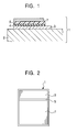
FIG. 1 shows a temperature-compensating thin-film
capacitor of a first embodiment of the present invention.
The thin-film capacitor 1 is formed by depositing a thin
first electrode layer (a lower electrode) 3, a second
dielectric thin-film 4, a first dielectric thin-film 5, and
a thin second electrode layer (an upper electrode) 7, in
that order on a rectangular surface of a substrate 2 when
shown in a plan view.
The substrate 2 may be composed of any material, as
long as the substrate 2 has an enough thickness to provide
proper stiffness to the entire capacitor and is resistant to
high temperatures while depositing the following layers or
films on the substrate 2: the first electrode layer 3; the
second dielectric thin-film 4; the first dielectric thin-film
5; and the second electrode layer 7. Materials that
satisfy the above condition are a silicon wafer, SiO2, Al2O3,
and so on.
The first electrode layer 3 and the second electrode
layer 7 may have a monolayer structure consisting of a
single metal such as Cu, Ag, Au, and Pt, or may have a
laminate structure consisting of a plurality of metal layers.
The laminate structure may be formed by depositing layers of
silicon oxide, elemental chromium, elemental nickel,
chromium oxide, nickel oxide, platinum, and so on.
The above second dielectric thin-film 4 preferably has
a high dielectric strength, a large Q factor, and a
capacitance-temperature coefficient which is smaller than
the coefficient of the first dielectric thin-film 5.
The second dielectric thin-film 4 preferably has
capacitance-temperature coefficient with an absolute value
of 50 ppm/°C or less. The second dielectric thin-film 4
preferably more preferably has capacitance-temperature
coefficient with an absolute value of 50 ppm/°C or less, a
specific inductive capacity of 10 or less, a field intensity
resistance of at least 5 MV/cm and more preferably at least
8 MV/cm, a nonloaded Q factor of at least 200 and more
preferably at least 500 at a frequency of at least 1 GHz,
and a dielectric relaxation time of at least 1 second. Also,
the second dielectric thin-film 4 preferably has a thickness
of 1 µm (1×10⁻⁶ m) or less and more preferably in the range
of 500 to 5,000 Å (0.05 to 0.5 µm), in order to achieve high
dielectric strength, miniaturization, and high productivity.
Materials that satisfy the above conditions are SiNx,
SiOx, amorphous SiOxNy, and so on. The SiNx layer may be
formed by film deposition such as PECVD. The amorphous
SiOxNy layer may be formed by film deposition such as
sputtering or PECVD.
The above first dielectric thin-film 5 may have a lower
dielectric strength, and preferably has a smaller linear
thermal expansion coefficient than the coefficient of the
second dielectric thin-film 4.
The first dielectric thin-film 5 preferably has a
specific inductive capacity of 4.0 or less and a linear
thermal expansion coefficient of 50 ppm/°C or more. The
first dielectric thin-film 5 more preferably has a specific
inductive capacity of 4.0 or less, a linear thermal
expansion coefficient of 50 ppm/°C or more, and a negative
capacitance-temperature coefficient. Further, the first
dielectric thin-film 5 more preferably has a specific
inductive capacity of 4.0 or less, a linear thermal
expansion coefficient of 50 ppm/°C or more, a negative
capacitance-temperature coefficient, and capacitance-temperature
coefficient with an absolute value of 200 ppm/°C
or more.
The thin-film capacitor preferably has a Q factor of at
least 100 and more preferably at least 300 at a frequency of
1 GHz or more when the first dielectric thin-film 5 is
placed between the first electrode layer 3 and the second
electrode layer 7.
Further, the first dielectric thin-film 5 preferably
has a specific inductive capacity in the range of 1.5 to 4.0
and more preferably 1.5 to 2.5.
The first dielectric thin-film 5 may contain, for
example, a fluoric polymer or at least one polymer selected
from the group consisting of polypropylene, polyether ether
ketone, and syndiotactic polystyrene as a main component.
The above fluoric polymer may be a crystalline
perfluoropolymer such as polytetrafluoroethylene,
tetrafluoroethylene-perfluoroalkylvinyl ether copolymer, or
tetrafluoroethylene-hexafluoropropylene copolymer, an
amorphous perfluoropolymer such as a cyclic polymer of
perfluorodivinyl ether, or a fluoric polymer such as
polychrolotrifluoroethylene, tetrafluoroethylene-ethylene
copolymer (ETFE), or chrolotrifluoroethylene-ethylene
copolymer. The cyclic polymer of perfluorodivinyl ether is
preferable in particular because the first dielectric thin-film
5 is easily formed by spin coating, spraying, or
dipping (soaking) and the resulting first dielectric thin-film
5 has a Q factor of 100 or more at a frequency of 1 GHz.
Also, the first dielectric thin-film 5 may contain a
benzocyclobutene polymer or a naphthocyclobutene polymer as
a main component. The benzocyclobutene polymer or a
naphthocyclobutene polymer has, for example, a
benzocyclobutene or naphthocyclobutene group and an ethylene
group, or a benzocyclobutene or naphthocyclobutene group, an
ethylene group, and a siloxane bond. A method for forming
the first dielectric thin-film 5 by using a benzocyclobutene
or naphthocyclobutene polymer is as follows, for example. A
solution containing a solvent and a monomer having
structural formula (I) is applied onto the surface of the
substrate 2, on which the first electrode layer 3 has been
formed, by spin coating, spraying, dipping (soaking) or the
like, and then the solvent is removed during curing on a hot
plate. Thus, the monomer is polymerized to form the first
dielectric thin-film 5 composed of the benzocyclobutene or
naphthocyclobutene polymer.
X1 ― CH = CH ― Y1 ― CH = CH ― X1
wherein X
1 represents
or
Y
1 represents a single bond, -CH
2-CH
2- , or -Si (R)
2-O-Si (R)
2-,
wherein R represents an alkyl group.
The first dielectric thin-film 5 preferably has a
thickness in the range of about 50 to 500 nm (500 to 5,000
Å).
Since the first dielectric thin-film 5 used for the
thin-film capacitor 1 of the first embodiment has a linear
thermal expansion coefficient of 50 ppm/°C or more, the
capacitance-temperature coefficient is made to have a
negative value. Also, the first dielectric thin-film 5 has
a specific inductive capacity of 4.0 or less, hence a
difference in specific inductive capacity according to
precision in processing is reduced and an accurate
temperature compensation is achieved. The first dielectric
thin-film 5 having a capacitance-temperature coefficient of
-200 ppm/°C or less is provided in order to adjust the
capacitance-temperature coefficient of the second dielectric
thin-film 4.
The Q factor, the voltage resistance, and the
capacitance-temperature coefficient of a capacitor are
controlled by adjusting the thickness and the composition of
the first dielectric thin-film 5 and the second dielectric
thin-film 4, so that devices having very stable
characteristics in an operating environment in which
temperature changes significantly are provided.
Also, the thin-film capacitor 1 has a multilayer
structure composed of the first dielectric thin-film 5 and
the second dielectric thin-film 4, that is, the structure of
the thin-film capacitor 1 is different from that of
conventional laminates composed of dielectric ceramic sheets.
Thus, thinning and miniaturization are easily achieved and a
capacitor having a thickness of 5 µm (5×10⁻⁶ m), for example,
is provided.
Further, if the first dielectric thin-film 5 is
composed of the above benzocyclobutene or naphthocyclobutene
polymer, it is not necessary to provide a protective coating
8 shown in the third embodiment described because such a
polymer is resistant to corrosion by a resist-developing
solution and a resist-peeling solution used for forming
electrodes.
As described above, the thin-film capacitor 1 shown in
FIG. 1 is useful for communication devices, portable
electronic devices such as mobile phones, and the like which
needs temperature compensation. The capacitor may be used
in combination with a varactor diode or an element
controlling a frequency according to a voltage.
Although the first dielectric thin-film 5 and the
second dielectric thin-film 4 are provided between the first
electrode layer 3 and the second electrode layer 7 in the
above embodiment, a thin-film capacitor 1a may have the
structure in which only the first dielectric thin-film 5 may
be provided between the first electrode layer 3 and the
second electrode layer 7 as shown in FIG. 8. In FIG. 8A,
reference numeral 2 represents a substrate.
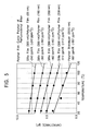
FIG. 3 illustrates an example that a thin-film
capacitor C1, which is the thin-film capacitor 1 of the
present invention, is placed in an electronic circuit. In
this circuit, a capacitor C0 is connected in series and a
varactor diode Dc is connected in parallel to a coil L, the
thin-film capacitor C1 is connected in parallel to the
varactor diode Dc, input terminals 11 and 12 are connected
to the upper electrode 7 and the lower electrode 3 of the
thin-film capacitor C1 shown in FIG. 1, and a resistor R is
placed between the input terminals 12 and either electrode
of the thin-film capacitor C1.
The varactor diode Dc shows a change in capacitance
according to voltage. The varactor diode Dc has a
predetermined positive capacitance-temperature coefficient,
so that a resonance circuit which is resistant to changes in
temperature is provided, in which the positive capacitance-temperature
coefficient compensates for the capacitance-temperature
coefficient of the thin-film capacitor C1.
Capacitance-temperature coefficients are shown in FIG.
4. When the varactor diode Dc has a capacitance-temperature
coefficient in the range of 200 to 500 ppm/°C, the
capacitance-temperature coefficient of the varactor diode
compensates for the capacitance-temperature coefficient of
the thin-film capacitor C1 which is in the range of -200 to -
500 ppm/°C. As a result, the temperature stability of the
circuit is improved. The conventional capacitors as
described above do not exhibit such a wide range of
capacitance-temperature coefficient.
The thin-film capacitor of the present invention is
applicable to temperature-compensating devices such as
temperature-compensating circuits of varactor diodes.
SECOND EMBODIMENT
FIG. 9 is a sectional view showing a temperature-compensating
thin-film capacitor of a second embodiment of
the present invention. In this embodiment, the second
dielectric thin-film 4 is deposited on the first dielectric
thin-film 5. The deposition order is different from that of
the first embodiment. The same components as those of the
first embodiment have the same reference number as the first
embodiment in this description.
The material of the second dielectric thin-film 4 is
selected from SiNx, SiOx, and SiOxNy, which are shown in the
first embodiment.
The material of the first dielectric thin-film 5 may
contain a fluoric polymer, a benzocyclobutene or
naphthocyclobutene polymer, or the like, which are the same
material as those used in the first embodiment.
In particular, when a material containing a fluoric
polymer such as a perfluorodivinyl ether polymer as a main
component is used for the first dielectric thin-film 5 of
this embodiment, it is preferable for the first dielectric
thin-film 5 that the second dielectric thin-film 4 covers
the first dielectric thin-film 5. That is, because the
above fluoric polymer is corroded by the resist-developing
solution and the resist-peeling solution used for forming
electrodes, forming the second dielectric thin-film 4 to
cover the first dielectric thin-film 5 prevents the first
dielectric thin-film 5 from corroding.
The thin-film capacitor 21 of the second embodiment has
the above structure, hence the thin-film capacitor 21
provides the same effect as the thin-film capacitor 1 of the
first embodiment.
THIRD EMBODIMENT
FIG. 10 is a sectional view showing a temperature-compensating
thin-film capacitor of the third embodiment of
the present invention. In this embodiment, a first
dielectric thin-film 5 which is deposited on a second
dielectric thin-film 4 containing the fluoric polymer as a
main component and a protective coating 8 is deposited on
and used to cover the first dielectric thin-film 5. The
same components as the first embodiment have the same
reference number as the first embodiment.
The material of the protective coating 8 is preferably
corrosion-resistant against a resist-developing solution and
a resist-peeling solution used for forming electrodes, and
is preferably selected from a group consisting of SiNx such
as Si3N4, SiOx such as SiO2, amorphous SiOxNy, Ti, and the
like.
The thin-film capacitor 31 of the second embodiment has
the above structure, hence the thin-film capacitor 31
provides the same effect as the thin-film capacitor 1 of the
first embodiment. The protective coating 8 is deposited on
the first dielectric thin-film 5 containing a fluoric
polymer as a main component to cover the first dielectric
thin-film 5, so that the first dielectric thin-film 5 is
prevented from corrosion which is caused by the resist-developing
solution and the resist-peeling solution used for
forming electrodes.
In FIG. 10, the protective coating 8, the second
dielectric thin-film 4, and the first dielectric thin-film 5
are placed between a first electrode layer 3 and a second
electrode layer 7. However, the first dielectric thin-film
5 and the protective coating 8 which is deposited thereon
may be placed between the first electrode layer 3 and the
second electrode layer 7 as shown in FIG. 11. A reference
numeral 2 in FIG. 11 represents a substrate.
EXAMPLES
Example 1
Q factors of various thin-film capacitors (samples 1 to
12) were measured as shown in Table 1. Each capacitor
included a dielectric thin-film placed between an upper
electrode and a lower electrode which were composed of
copper and were deposited on a substrate composed of alumina
or glass. Each thickness of the upper electrode and the
lower electrode was 1,500 nm (15,000 Å) and the thickness of
the dielectric thin-film was 2,000 nm (20,000 Å). The
length and width of the upper electrode were controlled
within the range of 50 to 1,000 µm in order to keep the
capacitance of the thin-film capacitor at 10 pF. The Q
factor, the specific inductive capacity, the linear thermal
expansion coefficient, the material for composing the thin-film,
and the evaluation of each sample is shown in Table 1.
| Samples | Material | Specific Inductive Capacity | Linear Thermal Expansion Coefficient | Q factor |
| | | (-) | Evalu. | (ppm/°C) | Evalu. | (-) |
| 1 | PTFE | 2.1 | Superior | 100 | Superior | 5,000 (at 10 GHz) |
| 2 | PFDE | 2.1 | Superior | 74 | Superior | 1,429 (at 10 GHz) |
| 3 | PFA | 2.1 | Superior | 120 | Superior | 3,333 (at 1 GHz) |
| 4 | FEP | 2.1 | Superior | 83 | Superior | 2,000 (at 1 GHz) |
| 5 | PCTFE | 2.3 to 2.5 | Superior | 70 | Superior | 100 (at 1 MHz) |
| 6 | ETFE | 2.6 | Superior | 90 | Superior | 200 (at 1 MHz) |
| 7 | ECTFE | 2.5 | Superior | 80 | Superior | 111 (at 1 MHz) |
| 8 | PP | 2.17 | Superior | 80 | Superior | 5,000 (at 10 GHz) |
| 9 | PEI | 3.1 | Superior | 23 | inferior | 159 (at 10 GHz) |
| 10 | PPS | 4.0 | Superior | 20 | inferior | 1,000 (at 1 MHz) |
| 11 | SPS | 2.9 | Superior | 25 | Superior | 213 (at 10 GHz) |
| 12 | PEEK | 3.1 | Superior | 48 | Superior | 455 (at 10 GHz) |
In Table 1, PTFE represents polytetrafluoroethylene,
PFDA represents a cyclic polymer of perfluorodivinyl ether,
PFA represents a polytetrafluoroethylene-perfluoroalkylvinyl
ether copolymer, FEP represents a tetrafluoroethylene-hexafluoropropylene
copolymer, PCTFE represents polychloro
trifluoroethylene, ETFE represents a tetrafluoroethylene-ethylene
copolymer, ECTFE represents a
chlorotrifluoroethylene-ethylene copolymer, PP represents
polypropylene, PEI represents polyetherimide, PPS represents
polyphenylenesulfide, SPS represents syndiotactic
polystyrene, and PEEK represents polyether ether ketone.
In Table 1, a material having a specific inductive
capacity of 4.0 or less is superior and a material having a
linear thermal expansion coefficient of 25 ppm/°C or more is
also superior, but a material having a linear thermal
expansion coefficient of less than 25 ppm/°C is inferior.
Table 1 shows that controlling the capacitance-temperature
coefficients of the dielectric thin-films of
Samples 9 and 10 to negative values is difficult because the
linear thermal expansion coefficients thereof are less than
25 ppm/°C. On the other hand, controlling the capacitance-temperature
coefficients of the dielectric thin-films of
Samples 1 to 8 and 11 to 12 in the negative range is
possible because the specific inductive capacity and the
linear thermal expansion coefficients thereof satisfy the
desired conditions. Also, the dielectric thin-films of
Samples 1 to 8 and 11 to 12 are hardly affected by
processing accuracy, hence, the dielectric thin-films have
small differences in capacitance. Although the Q factor
generally tends to decrease as the frequency increases, the
capacitors of Samples 1 to 4, 8 and 11 to 12 have Q factors
of 100 or more at a frequency of 1 GHz or more. That is,
the capacitors have excellent high frequency characteristics.
Example 2
A thin-film capacitor was prepared according to the
procedure described below. The thin-film capacitor had a
first and a second dielectric thin-film placed between
electrode layers and had a multilayer structure. A
capacitance-temperature coefficient, a Q factor at 1 GHz,
and a dielectric strength of a thin-film capacitor were
measured. The measurement was performed by varying the
thickness of the first dielectric thin-film within the range
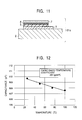
of 50 to 300 nm (500 to 3,000 Å). The capacitance-temperature
coefficient was determined according to the
slope of the plot of a capacitance (pF) versus temperature
(°C) varied in the range of 20 to 120 °C, as shown in FIG. 5.
The thicknesses of the first dielectric thin-film and the
second dielectric thin-film, and the capacitance-temperature
coefficient are shown in Table 2.
The thin-film capacitor was prepared as follows. A
copper lower electrode having a thickness of 1,500 nm
(15,000 Å) was deposited on an alumina or glass substrate by
sputtering; and then the dielectric thin-film which was
composed of SiNx and had a thickness of 300nm (3,000 Å) was
deposited on the lower electrode by PECVD.
Next, a solution which contains perfluorotributylamine
(TFPA) as a solvent and a cyclic polymer of perfluorodivinyl
ether was applied onto the second dielectric thin-film by a
spin coat method, and then the applied film was cured by (1)
curing at 50°C for 2 minutes, (2) curing at 110°C for 2
minutes, and (3) curing at 250°C for 10 minutes, if
necessary. The first dielectric thin-film composed of the
cyclic polymer of perfluorodivinyl ether was formed thereby
on the second dielectric thin-film. Subsequently, the first
dielectric thin-film was etched by 20 nm (200 Å) from the
surface in argon plasma using a dry etcher; a photoresist
pattern was formed on the polymer film by photoresist-coating,
pre-baking, exposing, developing, and post-baking;
the first dielectric thin-film and the second dielectric
thin-film were continuously etched with SF6 or CF4 by a
single process; and then the photoresist was removed.
Finally, a copper upper electrode layer having a thickness
of 1,500 nm (15,000 Å) was formed on the first dielectric
thin-film by sputtering at room temperature. The dielectric
thin-film having a multilayer structure was provided thereby.
The length and width of the upper electrode were controlled
within the range of 50 to 1,000 µm in order to keep the
capacitance of the thin-film capacitor at 10 pF. The thin-film
capacitor had a Q factor in the range of 210 to 290 at
a frequency of 1 GHz and a dielectric strength of 200 V or
more. The first dielectric thin-film had various Q factors
and dielectric strengths according to the thicknesses
thereof.
The SiNx second dielectric thin-film had a linear
thermal expansion coefficient of 3 ppm/°C and a specific
inductive capacity of 7.0. Also, the thin-film capacitor
had a Q factor of 200 at a frequency of 1 GHz when only the
second dielectric thin-film was formed between the electrode
layers.
The first dielectric thin-film composed of the cyclic
polymer of perfluorodivinyl ether had a linear thermal
expansion coefficient of 74 ppm/°C and a specific inductive
capacity of 2.1. Also, the thin-film capacitor had a
capacitance-temperature coefficient of -677 ppm/°C and a Q
factor of 300 at a frequency of 1 GHz when only the first
dielectric thin-film was formed between the electrode layers.
| Thickness of first dielectric thin-film | Thickness of second dielectric thin-film | Capacitance-temperature coefficient |
| (nm) | (nm) | (ppm/°C) |
| 50 | 300 | -240 |
| 100 | 300 | -360 |
| 200 | 300 | -462 |
| 300 | 300 | -512 |
FIG. 5 and Table 2 show that the capacitance-temperature
coefficient of the thin-film capacitor, which
comprises the second dielectric thin-film (a SiNx layer) and
the first dielectric thin-film (a polymer layer) both placed
between the electrodes, is controllable within the range of
-240 to -512 ppm/°C. The above coefficient is achieved by
varying the ratio of the thickness of the first dielectric
thin-film to that of the second dielectric thin-film. That
is, the thickness of the first dielectric thin-film is
varied in the range of 50 to 300 nm when the first
dielectric thin-film has a linear thermal expansion
coefficient of 74 ppm/°C and a specific inductive capacity
of 2.1. The thin-film capacitor of this embodiment is
suitable to a temperature-compensating electronic device
including a varactor diode having a positive capacitance-temperature
coefficient. Also, FIG. 5 and Table 2 show the
following results. Although the thin-film capacitor
including only the second dielectric thin-film between the
electrodes exhibits a Q factor of 200 at a frequency of 1
GHz, the thin-film capacitor of this embodiment including
the second dielectric thin-film and the first dielectric
thin-film which are both placed between the electrodes has a
Q factor of 210 or more at a frequency of 1 GHz.
Example 3
The relationship between the dimensional difference in
processing and the difference in capacitance of a thin-film
capacitor were measured while varying the dielectric
constant of the copper dielectric thin-film. The
dimensional difference in processing means the difference
between the actual size of a thin-film capacitor and the
design size. The difference in capacitance is caused by the
dimensional difference. In the above measurement, the
dielectric thin-films were placed between the lower
electrode and the upper electrode. The target sheet
capacitance of the thin-film capacitor was 10 pF. The
capacitance was determined according to equation (7) below:
Cs = ε0 × ε × (S/d)
wherein ε0 is 8.854×10⁻¹⁴ F•cm-1, S represents the area of the
electrodes, d represents the distance between the electrodes,
and ε represents the specific inductive capacity.
The dimensional difference in processing and the
difference in capacitance of a thin-film capacitor are shown
in Table 3. The capacitor included a dielectric thin-film
which was composed of ECTFE and had a specific inductive
capacity of 2.5, in which the electrode length L was 0.4 mm
and the interelectrode distance was 0.3 µm.
The dimensional difference in processing and the
difference in capacitance of the thin-film capacitor are
shown in Table 4. The capacitor included a dielectric thin-film
which was composed of PPS and had a specific inductive
capacity of 4, in which the electrode length L was 0.3 mm
and the interelectrode distance was 0.3 µm. The PPS
material used in this example had a specific inductive
capacity which was within the scope of the present invention,
but had a linear thermal expansion coefficient which was
outside of the scope of the present invention. Accordingly,
the PPS material was measured in order to only investigate
effects caused by the specific inductive capacity on the
difference in capacitance.
Table 5 shows the dimensional difference in processing
and difference in capacitance of a thin-film capacitor. The
thin-film capacitor had an electrode length L of 0.02 mm and
an interelectrode distance of 0.3 µm. The capacitor included
a BaTiO2 dielectric thin-film having a specific inductive
capacity of 1,000. The interelectrode distance is the same
as that of a thin-film capacitor having a specific inductive
capacity of 2.5 or 4.
Table 6 shows the dimensional difference in processing
and difference in capacitance of a thin-film capacitor. The
thin-film capacitor had an electrode length L of 0.3 mm and
an interelectrode distance of 80 µm. The capacitor included
a BaTiO
2 dielectric thin-film having a specific inductive
capacity of 1,000. The electrode area of the thin-film
capacitor is the same as that of a thin-film capacitor
having a specific inductive capacity of 4.
| Dimensional difference in processing | Cs | S | d | Difference in capacitance |
| (µm) | (pF) | (cm2) | (cm) | (±%) |
| 0 | 11.81 | 1.60×10⁻³ | 3.00×10⁻⁵ | 5 |
| 1 | 11.86 | 1.61×10⁻³ | 3.00×10⁻⁵ | 0.5 |
| 2 | 11.92 | 1.62×10⁻³ | 3.00×10⁻⁵ | 1.0 |
| 3 | 11.98 | 1.62×10⁻³ | 3.00×10⁻⁵ | 1.5 |
| 4 | 12.04 | 1.63×10⁻³ | 3.00×10⁻⁵ | 2.0 |
| 5 | 12.10 | 1.64×10⁻³ | 3.00×10⁻⁵ | 2.5 |
| 10 | 12.40 | 1.68×10⁻³ | 3.00×10⁻⁵ | 5.1 |
| L=0.4 mm, d=0.3 µm |
| Dimensional difference in processing | Cs | S | d | Difference in capacitance |
| (µm) | (pF) | (cm2) | (cm) | (±%) |
| 0 | 10.62 | 9.00×10⁻⁴ | 3.00×10⁻⁵ | 0 |
| 1 | 10.70 | 9.06×10⁻⁴ | 3.00×10⁻⁵ | 0.6 |
| 2 | 10.77 | 9.12×10⁻⁴ | 3.00×10⁻⁵ | 1.2 |
| 3 | 10.84 | 9.18×10⁻⁴ | 3.00×10⁻⁵ | 1.8 |
| 4 | 10.91 | 9.24×10⁻⁴ | 3.00×10⁻⁵ | 2.4 |
| 5 | 10.98 | 9.30×10⁻⁴ | 3.00×10⁻⁵ | 3.0 |
| 10 | 11.34 | 9.61×10⁻⁴ | 3.00×10⁻⁵ | 6.1 |
| L=0.3 mm, d=0.3 µm |
| Dimensional difference in processing | Cs | S | d | Difference in capacitance |
| (µm) | (pF) | (cm2) | (cm) | (±%) |
| 0 | 11.81 | 4.00×10⁻⁶ | 3.00×10⁻⁵ | 0 |
| 1 | 13.02 | 4.41×10⁻⁶ | 3.00×10⁻⁵ | 10.3 |
| 2 | 14.28 | 4.84×10⁻⁶ | 3.00×10⁻⁵ | 21.0 |
| 3 | 15.61 | 5.29×10⁻⁶ | 3.00×10⁻⁵ | 32.3 |
| 4 | 17.00 | 5.76×10⁻⁶ | 3.00×10⁻⁵ | 44.0 |
| 5 | 18.45 | 6.25×10⁻⁶ | 3.00×10⁻⁵ | 56.3 |
| 10 | 26.58 | 9.00×10⁻⁶ | 3.00×10⁻⁵ | 125.0 |
| L=0.02 mm, d=0.3 µm |
| Dimensional difference in processing | Cs | S | d | Difference in capacitance |
| (µm) | (pF) | (cm2) | (cm) | (±%) |
| 0 | 9.96 | 9.00×10⁻⁴ | 8.00×10⁻³ | 0 |
| 1 | 10.03 | 9.06×10⁻⁴ | 8.00×10⁻³ | 0.6 |
| 2 | 10.09 | 9.12×10⁻⁴ | 8.00×10⁻³ | 1.1 |
| 3 | 10.16 | 9.18×10⁻⁴ | 8.00×10⁻³ | 1.7 |
| 4 | 10.23 | 9.24×10⁻⁴ | 8.00×10⁻³ | 2.3 |
| 5 | 10.30 | 9.30×10⁻⁴ | 8.00×10⁻³ | 2.8 |
| 10 | 10.64 | 9.61×10⁻⁴ | 8.00×10⁻³ | 5.7 |
| L=0.3 mm, d=80 µm |
As shown in Tables 3 to 6, the difference in
capacitance significantly deviates from a tolerance range,
±5% of 10 pF, if the dimensional difference in processing is
1 µm or more, in which a thin-film capacitor includes a
dielectric thin-film having a specific inductive capacity of
1,000 and has the same interelectrode distance as that of a
thin-film capacitor including a dielectric thin-film having
a specific inductive capacity of 2.5 or 4. Also, the
difference in capacitance is inside the tolerance range if
the dimensional difference in processing is 5 µm or less, in
which a thin-film capacitor includes a dielectric thin-film
having a specific inductive capacity of 1,000 and has the
same electrode area as that of a capacitor including a
dielectric thin-film having a specific inductive capacity of
4. However, miniaturization of such a capacitor is
difficult because an interelectrode distance is 80 µm or
more.
On the other hand, as shown in Tables 3 and 4, the
difference in capacitance is inside the tolerance range if
the dimensional difference in processing is 5 µm or less, in
which a capacitor comprises a dielectric thin-film having a
specific inductive capacity of 2.5 or 4. Also, the
interelectrode distance of the thin-film capacitor having a
specific inductive capacity of 4 is 1/27 in comparison with
that of the thin-film capacitor having a specific inductive
capacity of 1,000, wherein the electrode area of both thin-film
capacitors is the same.
Accordingly, the difference in capacitance caused by
the dimensional difference in processing is reduced, and
miniaturization and thinning of a capacitor is possible if
the specific inductive capacity of the dielectric thin-film
is 4 or less.
Example 4
A thin-film capacitor was prepared according to the
procedure described below. The thin-film capacitor had a
first and a second dielectric thin-film placed between
electrode layers and had a multilayer structure. A
capacitance-temperature coefficient, a Q factor at 1 GHz,
and a dielectric strength of a thin-film capacitor were
measured. The capacitance-temperature coefficient was
determined according to the slope of the plot of a
capacitance (pF) versus temperature (°C) varied in the range
of 20 to 100 °C, as in FIG. 12.
The thin-film capacitor was prepared as follows. A
copper lower electrode having a thickness of 1,500nm (15,000
Å) was deposited on an alumina or glass substrate by
sputtering, and then the SiNx second dielectric thin-film
having a thickness of 150nm (1,500 Å) was deposited on the
lower electrode by PECVD.
Next, a solution which contains mesitylene as a solvent
and divinylsiloxane-bis-benzocyclobutene having formula (II)
below was applied onto the second dielectric thin-film by a
spin coat method, and then the applied film was cured by (1)
curing at 50°C for 2 minutes, (2) curing at 110°C for 2
minutes, and (3) curing at 250°C for 10 minutes, if
necessary. The polymer film of divinylsiloxane-bis-benzocyclobutene
having a thickness of 150 nm (1,500 Å) was
provided thereby.
Subsequently, a photoresist pattern was formed on the
polymer film of the second dielectric thin-film by
photoresist-coating, pre-baking, exposing, developing, and
post-baking; the first dielectric thin-film and the second
dielectric thin-film were continuously etched with SF6 or CF4
by a single process; and then the photoresist was removed.
Finally, a copper upper electrode layer having a thickness
of 1,500 nm (15,000 Å) was formed on the first dielectric
thin-film by sputtering at room temperature. The dielectric
thin-film having a multilayer structure was provided thereby.
The thin-film capacitor having a multilayer structure had a
Q factor of 100 at a frequency of 1 GHz, a dielectric
strength of 150 V or more, and a capacitance-temperature
coefficient of -261 ppm/°C.
The SiNx second dielectric thin-film had a linear
thermal expansion coefficient of 3 ppm/°C and a specific
inductive capacity of 7.0. Also, the thin-film capacitor
had a Q factor of 200 at a frequency of 1 GHz when only the
second dielectric thin-film was formed between the electrode
layers. The first dielectric thin-film composed of the
benzocyclobutene polymer had a linear thermal expansion
coefficient of 52 ppm/°C and a specific inductive capacity
of 2.7. Also, the thin-film capacitor had a capacitance-temperature
coefficient of -380 ppm/°C and a Q factor of 250
at a frequency of 1 GHz when only the first dielectric thin-film
was formed between the electrode layers.
The above result shows that the thin-film capacitor
having a capacitance-temperature coefficient of -261 ppm/°C
is provided when the capacitor has the second dielectric
thin-film composed of SiNx and the first dielectric thin-film
composed of the benzocyclobutene polymer which are both
placed between electrodes. Accordingly, the thin-film
capacitor of this example is applicable to a temperature-compensating
circuit of a varactor diode having a positive
capacitance-temperature coefficient because the capacitor
has a negative capacitance-temperature coefficient.
Also, the capacitor of this example has a Q factor of
100 or more, which is a large factor.
Example 5
A thin-film capacitor was prepared according to the
procedure described below. The thin-film capacitor had a
first and a second dielectric thin-film placed between
electrode layers and had a multilayer structure. A
capacitance-temperature coefficient, a Q factor at 1 GHz,
and a dielectric strength of a thin-film capacitor were
measured. The capacitance-temperature coefficient was
determined according to the slope of the plot of a
capacitance (pF) versus temperature (°C) varied in the range
of 20 to 100 °C, as in FIG. 13.
The thin-film capacitor was prepared as follows. A
copper lower electrode having a thickness of 1,500nm (15,000
Å) was deposited on an alumina or glass substrate by
sputtering, and then the SiNx second dielectric thin-film
having a thickness of 150nm (1,500 Å) was deposited on the
lower electrode by PECVD.
Next, a solution which contains mesitylene as a solvent
and divinylethyl-bis-naphthocyclobutene having formula (III)
below was applied onto the second dielectric thin-film by a
spin coat method, and then the applied film was cured by (1)
curing at 50°C for 2 minutes, (2) curing at 110°C for 2
minutes, and (3) curing at 250°C for 10 minutes, if
necessary. The polymer film of divinylethyl-bis-naphthocyclobutene
having a thickness of 150 nm (1,500 Å)
was provided thereby.
Subsequently, a photoresist pattern was formed on the
polymer film of the second dielectric thin-film by
photoresist-coating, pre-baking, exposing, developing, and
post-baking; the first dielectric thin-film and the second
dielectric thin-film were continuously etched with SF6 or CF4
by a single process; and then the photoresist was removed.
Finally, a copper upper electrode layer having a thickness
of 1,500 nm (15,000 Å) was formed on the first dielectric
thin-film by sputtering at room temperature. The dielectric
thin-film having a multilayer structure was provided thereby.
The thin-film capacitor having a multilayer structure had a
Q factor of 100 at a frequency of 1 GHz, a dielectric
strength of 150 V or more, and a capacitance-temperature
coefficient of -238 ppm/°C.
The second dielectric thin-film composed of SiNx had a
linear thermal expansion coefficient of 3 ppm/°C and a
specific inductive capacity of 7.0. Also, the second
dielectric thin-film had a Q factor of 200 at a frequency of
1 GHz when only the second dielectric thin-film was formed
between the electrode layers. The first dielectric thin-film
composed of the naphthocyclobutene polymer had a linear
thermal expansion coefficient of 50 ppm/°C and a specific
inductive capacity of 2.75. Also, the first dielectric
thin-film had a capacitance-temperature coefficient of -370
ppm/°C and a Q factor of 240 at a frequency of 1 GHz when
only the first dielectric thin-film was formed between the
electrode layers.
The above result shows that a thin-film capacitor
having a capacitance-temperature coefficient of -238 ppm/°C
is provided when the capacitor has the second dielectric
thin-film composed of SiNx and the first dielectric thin-film
composed of the naphthocyclobutene polymer which are
both placed between electrodes. Accordingly, the thin-film
capacitor of this example is applicable to a temperature-compensating
circuit of a varactor diode having a positive
capacitance-temperature coefficient because the capacitor
has a negative capacitance-temperature coefficient.
Also, the capacitor of this example has a Q factor of
100 or more, which is a large factor.
Example 6
A thin-film capacitor was prepared according to the
procedure described below. The thin-film capacitor had a
first and a second dielectric thin-film placed between
electrode layers and had a multilayer structure. A
capacitance-temperature coefficient, a Q factor at 1 GHz,
and a dielectric strength of a thin-film capacitor were
measured. The capacitance-temperature coefficient was
determined according to the slope of the plot of a
capacitance (pF) versus temperature (°C) varied in the range
of 20 to 100 °C, as in FIG. 14.
The thin-film capacitor was prepared as follows. A
copper lower electrode having a thickness of 1,500nm (15,000
Å) was deposited on an alumina or glass substrate by
sputtering, and then the SiNx second dielectric thin-film
having a thickness of 150nm (1,500 Å) was deposited on the
lower electrode by PECVD.
Next, a solution which contains mesitylene as a solvent
and divinylsiloxane-bis-naphthocyclobutene having formula
(IV) below was applied onto the second dielectric thin-film
by a spin coat method, and then the applied film was cured
by (1) curing at 50°C for 2 minutes, (2) curing at 110°C for
2 minutes, and (3) curing at 250°C for 10 minutes, if
necessary. The polymer film of divinylethyl-bis-naphthocyclobutene
having a thickness of 150 nm (1,500 Å)
was provided thereby.
Subsequently, a photoresist pattern was formed on the
polymer film of the second dielectric thin-film by
photoresist-coating, pre-baking, exposing, developing, and
post-baking; the first dielectric thin-film and the second
dielectric thin-film were continuously etched with SF6 or CF4
by a single process; and then the photoresist was removed.
Finally, a copper upper electrode layer having a thickness
of 1,500 nm (15,000 Å) was formed on the first dielectric
thin-film by sputtering at room temperature. The dielectric
thin-film having a multilayer structure was provided thereby.
The thin-film capacitor having a multilayer structure had a
Q factor of 100 at a frequency of 1 GHz, a dielectric
strength of 150 V or more, and a capacitance-temperature
coefficient of -243 ppm/°C.
The second dielectric thin-film composed of SiNx had a
linear thermal expansion coefficient of 3 ppm/°C and a
specific inductive capacity of 7.0. Also, the second
dielectric thin-film had a Q factor of 200 at a frequency of
1 GHz when only the second dielectric thin-film was formed
between the electrode layers. The first dielectric thin-film
composed of the naphthocyclobutene polymer had a linear
thermal expansion coefficient of 50 ppm/°C and a specific
inductive capacity of 2.8. Also, the first dielectric thin-film
had a capacitance-temperature coefficient of -373
ppm/°C and a Q factor of 230 at a frequency of 1 GHz when
only the first dielectric thin-film was formed between the
electrode layers.
The above result shows that a thin-film capacitor
having a capacitance-temperature coefficient of -243 ppm/°C
is provided when the capacitor has the second dielectric
thin-film composed of SiNx and the first dielectric thin-film
composed of the naphthocyclobutene polymer which are
both placed between electrodes. Accordingly, the thin-film
capacitor of this example is applicable to a temperature-compensating
circuit of a varactor diode having a positive
capacitance-temperature coefficient because the capacitor
has a negative capacitance-temperature coefficient.
Also, the capacitor of this example has a Q factor of
100 or more, which is a large factor.