FIELD OF THE INVENTION
The present invention relates to a semiconductor laser apparatus, and a
semiconductor laser module, having a structure in which structures for implementing a
desirable optical output power and a high energy conversion efficiency from input electric
power to output optical power are adequately combined.
BACKGROUND OF THE INVENTION
Recently, with widespread use of various communication media such as the
Internet, there have been increased demands for optical communication to be greater in
capacity. In the optical communication in the past, at respective bands of wavelengths
1310 nm and 1550 nm where the absorption of light by an optical fiber is small, the
transmission generally was performed by a single wavelength. In this system, for a
greater quantity of information to be transmitted, it was necessary to install a greater
number of cores of optical fibers in the transmission path, with increase in cost following
increase in transmission capacity, as a problem.
For this reason, there has been applied a WDM (wavelength division
multiplexing) communication system. The WDM communication system mainly
employs an EDFA (Erbium Doped Fiber Amplifier), which is for a system that has a
1530-1570 nm band as an operation band, where it uses a plurality of wavelengths to
perform transmission. This DWDM communication system or WDM communication
system uses a single optical fiber for concurrent transmission of a plurality of optical
signals different in wavelength, allowing for the network to have a greatly increased
transmission capacity, without needing the installation of additional optical fiber lines
(i.e., "new lines").
For excitation of the EDFA, there have been employed high-output pumping
semiconductor laser modules. Among them, the 1480nm-band pumping semiconductor
laser module has advantages, such as 1) high reliability, 2) high conversion efficiency of
erbium doped fiber, with merit in adaptation for the amplifier to be high of output, 3)
wide absorption band of erbium doped fiber, enabling synthesis at multiple wavelengths,
and 4) availability of peripheral optics such as isolators, wavelength synthesizers, and
polarization synthesizers. As a result, by the use of wavelength synthesis, polarization
synthesis, and the like, and by use of a plurality of pumping semiconductor laser modules,
there has been implemented an pumping light source for high-output optical fiber
amplifiers, and adapted for use in an optical fiber amplification system.
In general, in the semiconductor laser device (as a semiconductor laser
apparatus), when injected electric current is increased, the optical output power increases.
However, due to heat dissipation of the semiconductor laser device itself, a saturation in
output power appears at a certain driving current, and thereafter the optical output power
will not increase even with an increased driving current.
For the saturating driving current to be increased in value, the semiconductor
laser apparatus had a cavity length elongated so that a desirable optical output power was
obtained. On the contrary, to reduce the driving current required to obtain a desirable
optical output power, there was selected an adequate cavity length, so that a
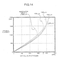
semiconductor laser apparatus was configured with the selected cavity length. Fig. 14 is a
graph showing a driving current vs. optical output power relationship for the cavity length
of semiconductor laser apparatus taken as a parameter. For example, in case of a
semiconductor laser apparatus to be adapted for an optical output power of 360 mW, a
cavity length of 1200µm was adopted so that the driving current was minimized in Fig.
14.
However, elongation of the cavity length in semiconductor laser apparatus
accompanied variation in physical configuration of the semiconductor laser apparatus,
with a result that, in case of determination of the cavity length of semiconductor laser
apparatus simply depending on driving current, the electric drive power involved
increases, not simply in electric power consumed for optical output power of the
semiconductor laser apparatus, but also of reactive power consumed at other parts in the
semiconductor laser apparatus itself, such as due to serial resistance and thermal
resistance, sometimes causing, as a problem, a reduction of the photoelectric power
conversion efficiency. (The photoelectric power conversion efficiency is often defined as
an optical output power of a semiconductor laser apparatus divided by electric drive
power of the semiconductor laser apparatus.)
Moreover, with increase in reactive power consumed by semiconductor laser
apparatus, that is, in the difference between electric drive power and optical output power,
which is mainly converted to heat, there was the need for a heat dissipating structure to be
large, resulting in a large-sized semiconductor laser module for incorporation of the
semiconductor laser apparatus, as a problem. The prior art has not investigated or
considered selecting the value of the cavity length to minimize the electric drive power or
to maximize the photoelectric conversion efficiency for a given optical output power. In
addition, the prior art has not investigated or considered selecting the value of other laser
parameters, such as an impurity carrier concentration in an upper cladding layer of the
laser, to minimize input drive power or to maximize conversion efficiency.
SUMMARY OF THE INVENTION
The present invention has been made with such points in view. It therefore is an
object of the present invention to provide, in implementation of a semiconductor laser
apparatus adapted for a desirable optical output power, a semiconductor laser apparatus
having its electric drive power rendered minimal or its photoelectric conversion efficiency
rendered maximal, as well as a fabrication method of the same, and a semiconductor laser
module with the same. (The photoelectric conversion efficiency is the energy conversion
efficiency of electrical power to optical power.)
To achieve the object, according to a first aspect of the invention, there is
provided a semiconductor laser apparatus wherein a respective element value of the
semiconductor laser apparatus is determined on the basis of relationships between
respective elements of the semiconductor laser apparatus including a cavity length of the
semiconductor laser apparatus and a carrier concentration of an upper cladding layer of
the semiconductor laser apparatus and a photoelectric conversion efficiency or electric
drive power of the semiconductor laser apparatus, for optical output power to be constant
as a parameter, so that the electric drive power is vicinal to a minimum thereof or the
photoelectric conversion efficiency is vicinal to a maximum thereof in correspondence to
a desirable optical output power. An exemplary vicinal value is preferably within 10% of
the minimum of the drive power and within 10% of the maximum of the conversion
efficiency, and more preferably within 6% thereof, and most preferably within 3%
thereof.
According to the first aspect of the invention, by implementation of a
semiconductor laser apparatus wherein a respective element value of the semiconductor
laser apparatus is determined on the basis of relationships between respective elements of
the semiconductor laser apparatus including a cavity length of the semiconductor laser
apparatus and a carrier concentration of an upper cladding layer of the semiconductor
laser apparatus and a photoelectric conversion efficiency or electric drive power of the
semiconductor laser apparatus, for optical output power to be constant as a parameter, so
that the electric drive power is vicinal to a minimum thereof or the photoelectric
conversion efficiency is vicinal to a maximum thereof in correspondence to a desirable
optical output power, it is enabled to obtain an desirable optical output power in a range
over 50 mW, with a photoelectric conversion efficiency in a vicinity of a maximum or
electric drive power in a vicinity of a minimum.
According to the second aspect of the invention, there is provided a
semiconductor laser apparatus wherein a cavity length over 1000 µm is determined on the
basis of a relationship of electric drive power to a range of optical output power over
50 mW, for cavity length to be constant as a parameter in a range over 1000 µm, so that
the electric drive power is vicinal to a minimum thereof in correspondence to a desirable
optical output power.
According to the second aspect of the invention, by implementation of a
semiconductor laser apparatus wherein a cavity length over 1000 µm is determined on the
basis of a relationship of electric drive power to a range of optical output power over
50 mW, for cavity length to be constant as a parameter in a range over 1000 µm, so that
the electric drive power is vicinal to a minimum thereof in correspondence to a desirable
optical output power, it is enabled to obtain an desirable optical output power in a range
over 50 mW, with electric drive power in a vicinity of a minimum.
According to a third aspect of the invention, there is provided a semiconductor
laser apparatus wherein a cavity length is determined on the basis of a relationship of a
photoelectric conversion efficiency to a range of cavity length over 1000 µm, for optical
output power to be constant as a parameter in a range over 50 mW, so that the
photoelectric conversion efficiency is vicinal to a maximum thereof in correspondence to
a desirable optical output power.
According to the third aspect of the invention, by implementation of a
semiconductor laser apparatus wherein a cavity length is determined on the basis of a
relationship of a photoelectric conversion efficiency to a range of cavity length over
1000 µm, for optical output power to be constant as a parameter in a range over 50 mW,
so that the photoelectric conversion efficiency is vicinal to a maximum thereof in
correspondence to a desirable optical output power, it is enabled to obtain an desirable
optical output power in a range over 50 mW, with high photoelectric conversion
efficiency.
According to a fourth aspect of the invention, in the above semiconductor laser
apparatus, the cavity length is determined on the basis of an approximation expression
making the photoelectric conversion efficiency maximal in correspondence to the
desirable optical output power.
According to the fourth aspect of the invention, determination of the cavity
length is based an approximation expression making the photoelectric conversion
efficiency maximal in correspondence to the desirable optical output power.
According to a fifth aspect of the invention, in the above semiconductor laser
apparatus, a cavity length over 1000 µm is determined on the basis of a relationship of
electric drive power to a range of cavity length over 1000 µm, for optical output power to
be constant as a parameter in a range over 50 mW, so that the electric drive power is
vicinal to a minimum thereof in correspondence to a desirable optical output power.
According to the fifth aspect of the invention, by implementation of a
semiconductor laser apparatus having a cavity length over 1000 µm determined on the
basis of a relationship of electric drive power to a range of cavity length over 1000 µm,
for optical output power to be constant as a parameter in a range over 50 mW, so that the
electric drive power is vicinal to a minimum thereof in correspondence to a desirable
optical output power, it is enabled to obtain an desirable optical output power in a range
over 50 mW, with low electric drive power.
According to a sixth aspect of the invention, in the above semiconductor laser
apparatus, the cavity length is determined on the basis of an approximation expression
making the electric drive power minimal in correspondence to the desirable optical output
power.
According to the sixth aspect of the invention, when the cavity length is
determined, it is determined on the basis of an approximation expression making an
electric drive power minimal in correspondence to the desirable optical output power.
According to a seventh aspect of the invention, in the above semiconductor laser
apparatus, an active layer forming a cavity with the cavity length has a strain multiple
quantum well structure.
According to the seventh aspect of the invention, as an active layer forming a
cavity with the cavity length, there is applied a strain multiple quantum well structure,
while it is enabled even for the semiconductor laser apparatus having a strain multiple
quantum well structure to obtain an desirable optical output power in a range over
50 mW, with high photoelectric conversion efficiency or low electric drive power.
According to an eighth aspect of the invention, in the above semiconductor laser
apparatus, the desirable optical output power is within a range of 50 mW to 400 mW, and
the cavity length is within a range of 1000 µm to 1800 µm, and more preferably within a
range of 1000 µm to 1600 µm.
According to the eighth aspect of the invention, there is implemented a concrete
semiconductor laser apparatus to be distinctive, particularly when letting the desirable
optical output power be within a range of 50 mW to 400 mW and the cavity length be
within a range of 1000 µm to 1800 µm, and more preferably within a range of 1000 µm to
1600 µm, and determining the cavity length simply from the relationship of the electric
drive power to the optical output power.
According to a ninth aspect of the invention, in the above semiconductor laser
apparatus, the desirable optical output power is within a range of 50 mW to 200 mW, and
the cavity length is within a range of 1000 µm to 1400 µm.
According to the ninth aspect of the invention, there is implemented a concrete
semiconductor laser apparatus to be distinctive, particularly when letting the desirable
optical output power be within a range of 50 mW to 200 mW and the cavity length be
within a range of 1000 µm to 1400 µm, and determining the cavity length simply from the
relationship of the electric drive power to the optical output power.
According to a tenth aspect of the invention, in the semiconductor laser
apparatus, an upper cladding layer has an impurity carrier concentration determined on
the basis of a relationship of a photoelectric conversion efficiency or electric drive power
to the impurity carrier concentration of the upper cladding layer, for optical output power
and cavity length to be constant as parameters, so that the electric drive power is vicinal
to a minimum thereof or the photoelectric conversion efficiency is vicinal to a maximum
thereof in correspondence to a desirable optical output power.
According to the tenth aspect of the invention, by implementation of a
semiconductor laser apparatus, an upper cladding layer has an impurity carrier
concentration determined on the basis of a relationship of a photoelectric conversion
efficiency or electric drive power to the impurity carrier concentration of the upper
cladding layer, for optical output power and cavity length to be constant as parameters, so
that the electric drive power is vicinal to a minimum thereof or the photoelectric
conversion efficiency is vicinal to a maximum thereof in correspondence to a desirable
optical output power, it is enabled to obtain an desirable optical output power in a range
over 50 mW, with a photoelectric conversion efficiency in a vicinity of a maximum or
electric drive power in a vicinity of a minimum.
According to an eleventh aspect of the invention, there is provided a
semiconductor laser module comprising a semiconductor laser apparatus according to any
of the first to tenth aspects of the invention, an optical fiber for conducting outside laser
light projected from the semiconductor laser apparatus, and an optical coupling lens
system for an optical coupling between the semiconductor laser apparatus and the optical
fiber.
According to the eleventh aspect of the invention, by implementation of a
semiconductor laser module with an incorporated semiconductor laser apparatus
according to any of the first to tenth aspects of the invention, it is enabled to obtain an
desirable optical output power, with high photoelectric conversion efficiency or low
electric drive power.
According to a twelfth aspect of the invention, the above semiconductor laser
module further comprises a temperature controller for controlling a temperature of the
semiconductor laser apparatus, and an optical fiber grating formed in a vicinity of an
incidence end of the optical fiber.
According to the twelfth aspect of the invention, an optical fiber grating is
formed in a vicinity of an incidence end of the optical fiber, and laser light of a
wavelength selected by the optical fiber grating is output.
According to a thirteenth aspect of the invention, the above semiconductor laser
module further comprises a temperature controller for controlling a temperature of the
semiconductor laser apparatus, and an isolator disposed in the optical coupling lens
system, for suppressing an incidence of reflection return light from an optical fiber side.
According to the thirteenth aspect of the invention, by implementation of a
semiconductor laser module with an incorporated semiconductor laser apparatus
according to any of the first to tenth aspects of the invention, it is enabled even for the
semiconductor laser module with an incorporated temperature controller to obtain an
desirable optical output power, with high photoelectric conversion efficiency or low
electric drive power.
According to a fourteenth aspect of the invention, there is provided a fabrication
method for a semiconductor laser apparatus, comprising a relationship acquiring step for
acquiring relationships between respective elements of the semiconductor laser apparatus
including a cavity length of the semiconductor laser apparatus and a carrier concentration
of an upper cladding layer of the semiconductor laser apparatus and a photoelectric
conversion efficiency or electric drive power of the semiconductor laser apparatus, for
optical output power to be constant as a parameter, an element value determining step for
determining a respective element value of the semiconductor laser apparatus to be
determined on the basis of the relationships acquired by the relationship acquiring step, so
that the electric drive power is vicinal to a minimum thereof or the photoelectric
conversion efficiency is vicinal to a maximum thereof in correspondence to a desirable
optical output power, and a forming step for forming the semiconductor laser apparatus
having the respective element value determined by the element value determining step.
According to the fourteenth aspect of the invention, for fabrication of a
semiconductor laser apparatus, in a relationship acquiring step there are acquired
relationships between respective elements of the semiconductor laser apparatus including
a cavity length of the semiconductor laser apparatus and a carrier concentration of an
upper cladding layer of the semiconductor laser apparatus and a photoelectric conversion
efficiency or electric drive power of the semiconductor laser apparatus, for optical output
power to be constant as a parameter, in an element value determining step there is
determined a respective element value of the semiconductor laser apparatus to be
determined on the basis of the relationships acquired by the relationship acquiring step, so
that the electric drive power is vicinal to a minimum thereof or the photoelectric
conversion efficiency is vicinal to a maximum thereof in correspondence to a desirable
optical output power, and in a forming step there is formed the semiconductor laser
apparatus having the respective element value determined by the element value
determining step.
According to a fifteenth aspect of the invention, there is provided a fabrication
method for a semiconductor laser apparatus, comprising a relationship acquiring step for
acquiring a relationship of electric drive power to a range of optical output power power
over 50 mW, for cavity length to be constant as a parameter in a range over 1000 µm, a
cavity length determining step for determining a cavity length over 1000 µm to be
determined on the basis of the relationship acquired by the relationship acquiring step, so
that the electric drive power is vicinal to a minimum thereof in correspondence to a
desirable optical output power, and a forming step for forming the semiconductor laser
apparatus having the cavity length determined by the cavity length determining step.
According to the fifteenth aspect of the invention, for fabrication of a
semiconductor laser apparatus, in a relationship acquiring step there is acquired a
relationship of electric drive power to a range of optical output power over 50 mW, for
cavity length to be constant as a parameter in a range over 1000 µm, in a cavity length
determining step there is determined a cavity length over 1000 µm to be determined on
the basis of the relationship acquired by the relationship acquiring step, so that the electric
drive power is vicinal to a minimum thereof in correspondence to a desirable optical
output power, and in a forming step there is formed the semiconductor laser apparatus
having the cavity length determined by the cavity length determining step.
According to a sixteenth aspect of the invention, there is provided a fabrication
method for a semiconductor laser apparatus, comprising a relationship acquiring step for
acquiring a relationship of a photoelectric conversion efficiency to a range of cavity
length over 1000 µm, for optical output power to be constant as a parameter in a range
over 50 mW, a cavity length determining step for determining a cavity length to be
determined on the basis of the relationship acquired by the relationship acquiring step, so
that the photoelectric conversion efficiency is vicinal to a maximum thereof in
correspondence to a desirable optical output power, and a forming step for forming the
semiconductor laser apparatus having the cavity length determined by the cavity length
determining step.
According to the sixteenth aspect of the invention, for fabrication of a
semiconductor laser apparatus, in a relationship acquiring step there is acquired a
relationship of a photoelectric conversion efficiency to a range of cavity length over
1000 µm, for optical output power to be constant as a parameter in a range over 50 mW,
in a cavity length determining step there is determined a cavity length to be determined
on the basis of the relationship acquired by the relationship acquiring step, so that the
photoelectric conversion efficiency is vicinal to a maximum thereof in correspondence to
a desirable optical output power, and in a forming step there is formed the semiconductor
laser apparatus having the cavity length determined by the cavity length determining step.
According to a seventeenth aspect of the invention, the above fabrication method
for a semiconductor laser apparatus further comprises an approximation expression
calculating step for determining an approximation expression for making the
photoelectric conversion efficiency maximal in correspondence to the desirable optical
output power, on the basis of the relationship acquired by the relationship acquiring step,
and the cavity length determining step determining the cavity length on the basis of the
approximation expression.
According to the seventeenth aspect of the invention, an approximation
expression calculating step determines an approximation expression for making the
photoelectric conversion efficiency maximal in correspondence to the desirable optical
output power, on the basis of the relationship acquired by the relationship acquiring step,
and the cavity length determining step determines the cavity length on the basis of the
approximation expression.
According to an eighteenth aspect of the invention, there is provided a
fabrication method for a semiconductor laser apparatus, comprising a relationship
acquiring step for acquiring a relationship of electric drive power to a range of cavity
length over 1000 µm, for optical output power to be constant as a parameter in a range
over 50 mW, a cavity length determining step for determining a cavity length over
1000 µm to be determined on the basis of the relationship acquired by the relationship
acquiring step, so that the electric drive power is vicinal to a minimum thereof in
correspondence to a desirable optical output power, and a forming step for forming the
semiconductor laser apparatus having the cavity length determined by the cavity length
determining step.
According to the eighteenth aspect of the invention, for fabrication of a
semiconductor laser apparatus, in a relationship acquiring step there is acquired a
relationship of electric drive power to a range of cavity length over 1000 µm, for optical
output power to be constant as a parameter in a range over 50 mW, in a cavity length
determining step there is determined a cavity length over 1000 µm to be determined on
the basis of the relationship acquired by the relationship acquiring step, so that the electric
drive power is vicinal to a minimum thereof in correspondence to a desirable optical
output power, and in a forming step there is formed the semiconductor laser apparatus
having the cavity length determined by the cavity length determining step.
According to a nineteenth aspect of the invention, the above fabrication method
for a semiconductor laser apparatus further comprises an approximation expression
calculating step for determining an approximation expression for making the electric
drive power minimal in correspondence to the desirable optical output power, on the basis
of the relationship acquired by the relationship acquiring step, and the cavity length
determining step determining the cavity length on the basis of the approximation
expression.
According to the nineteenth aspect of the invention, an approximation expression
calculating step determines an approximation expression for making the electric drive
power minimal in correspondence to the desirable optical output power, on the basis of
the relationship acquired by the relationship acquiring step, and the cavity length
determining step determines the cavity length on the basis of the approximation
expression.
According to a twentieth aspect of the invention, in the above fabrication method
for a semiconductor laser apparatus, an active layer forming a cavity with the cavity
length has a strain multiple quantum well structure.
According to the twentieth aspect of the invention, as an active layer forming a
cavity with the cavity length there is applied a strain multiple quantum well structure,
while it is enabled even for the semiconductor laser apparatus having a strain multiple
quantum well structure to obtain an desirable optical output power in a range over
50 mW, with high photoelectric conversion efficiency or low electric drive power.
According to a twenty-first aspect of the invention, there is provided a
fabrication method for a semiconductor laser apparatus, comprising a relationship
acquiring step for acquiring a relationship of electric drive power to an impurity carrier
concentration of an upper cladding layer, for optical output power and cavity length to be
constant as parameters, a carrier concentration determining step for determining the
impurity carrier concentration to be determined on the basis of the relationship acquired
by the relationship acquiring step, so that the electric drive power is vicinal to a minimum
thereof in correspondence to a desirable optical output power; and a forming step for
forming the semiconductor laser apparatus with the upper cladding layer having the
impurity carrier concentration thereof set to the impurity carrier concentration determined
by the carrier concentration determining step.
According to the twenty-first aspect of the invention, for fabrication of a
semiconductor laser apparatus, in a relationship acquiring step there is acquired a
relationship of electric drive power to an impurity carrier concentration of an upper
cladding layer, for optical output power and cavity length to be constant as parameters, in
a carrier concentration determining step there is determined the impurity carrier
concentration to be determined on the basis of the relationship acquired by the
relationship acquiring step, so that the electric drive power is vicinal to a minimum
thereof in correspondence to a desirable optical output power, and in a forming step there
is formed the semiconductor laser apparatus with the upper cladding layer having the
impurity carrier concentration thereof set to the impurity carrier concentration determined
by the carrier concentration determining step.
Other objects and features of this invention will become understood from the
following description with reference to the accompanying drawings.
BRIEF DESCRIPTION OF THE DRAWINGS
The above and further objects and novel features of the present invention will
more fully appear from the following detailed description when the same is read in
conjunction with the accompanying drawings, in which:
DESCRIPTION OF THE PREFERRED EMBODIMENTS
There will be detailed below the preferred embodiments of a semiconductor laser
apparatus and a fabrication method of the same, and a semiconductor laser module
according to the present invention, with reference made to the accompanying drawings.
First embodiment
First, description is made of a first embodiment of the invention. Fig. 1 is a
broken perspective view of a schematic arrangement of a semiconductor laser apparatus
according to the first embodiment of the invention, Fig. 2, a longitudinal sectional view of
the semiconductor laser apparatus of Fig. 1, and Fig. 3, a sectional view along line A-A of
the semiconductor laser apparatus of Fig. 2. As in Fig. 1 to Fig. 3, this semiconductor
laser apparatus 20 has laminated on a surface of an n-InP substrate 1, in sequence, an n-InP
cladding layer 2 concurrently serving as a buffer layer and a lower cladding layer by
n-InP, a GRIN-SCH-MQW (Graded Index-Separate Confinement Heterostructure Multi
Quantum Well) active layer 3 with compression strains, a p-InP clad layer 6, and an
InGaAsP cap layer 7.
Part of the p-InP cladding layer 6, the GIN-SCH-MQW active layer 3, and an
upper part of the n-InP cladding layer 2 are processed in a mesa stripe form, and both
sides of the mesa stripe are buried by a p-InP blocking layer 8 and an n-InP blocking layer
9 that are formed as current blocking layers. Upside of the InGaAs cap layer 7 is formed
a p-side electrode 10, and downside of the n-InP substrate 1 is formed an n-side electrode
11.
On a light reflective rear facet as one facet in a longitudinal direction of the
semiconductor laser apparatus 20 is formed a reflective film 14 with a high light
reflectivity of over a 80%, and on a light emitting front facet as the other facet is formed a
low reflectivity film 15 with a reflectivity within a range of 1% to 5%, and preferably less
than 4%. Light is generated in the GRIN-SCH-MQW active layer 3 and amplified in the
cavity formed by the rear facet and the front facet, and is emitted as laser light through the
front facet.
The GRIN-SCH layer comprises two quaternary GaInAsP layers of bandgap-wavelength
of 1.1 µm and 1.2 µm, total thickness of about 40 nm for each side. Well
layers of MQW comprise 4nm-thick quaternary GaInAsP layers with in-plane
compressive strain of about 1%. Barrier layers of MQW comprise quaternary GaInAsP
layers of bandgap-wavelength of 1.2 µm, thickness of 10 nm each. Other conditions for
the well thickness larger than 3.4 nm and strain amount larger than 0.5% can be adopted
so far as desired lasing wavelength can be obtained. The layer structure for the GRIN-SCH
layers can also be modified in the range of total thickness of 20-50 nm.
The GRIN-SCH-MQW active layer 3 has its longitudinal length as a cavity
length L to be set 1000µm or greater. Optical output power from the semiconductor laser
apparatus 20 is set to be 50 mW or greater.
The cavity length L of the semiconductor laser apparatus shown in Fig. 1 is
determined on the basis of a relationship shown in Fig. 4. Fig. 4 is a graph showing a
relationship of electric drive power to an optical output power for cavity length taken as a
parameter. Fig. 4 shows the relationship between drive power and optical output power
for cavity lengths of 800µm, 1000µm, 1300µm, 1500µm, and 1800µm, on the assumption
that the semiconductor laser apparatus 20 has a structure shown in Fig. 1.
As in Fig. 4, in general, semiconductor laser apparatus short of cavity length
needs greater electric drive power to obtain a specified optical output power, in
comparison with semiconductor laser apparatus long of cavity length. However,
comparison between cavity lengths 1500µm and 1800µm shows an inversion in a vicinity
(P1) of a 420 mW optical output power, revealing that, for an optical output power to be
420 mW or greater, a semiconductor laser apparatus with the longer cavity length
1800µm suffices with lower drive power. Likewise, comparison between cavity lengths
1300µm and 1800µm shows an inversion in a vicinity (P2) of a 350 mW optical output
power, revealing that, for an optical output power to be 350 mW or greater, a
semiconductor laser apparatus with the longer cavity length 1800µm suffices with lower
drive power. Still more, comparison between cavity lengths 1000µm and 1800µm shows
an inversion in a vicinity (P3) of a 250 mW optical output power, revealing that, for an
optical output power to be 250 mW or greater, a semiconductor laser apparatus with the
longer cavity length 1800µm suffices with lower drive power. In other words, for a
specified optical output power to be obtained, the cavity length has an optimal value for
the drive power to be minimal, which is variable with the specified value of optical output
power.
It is now supposed that the cavity length was selected on the basis of a
conventional relationship of driving current to optical output power shown in Fig. 14.
Because it was assumed in the past that the smaller the driving current of a semiconductor
laser apparatus was, the smaller the drive power of the semiconductor laser apparatus
should have been, there were to be selected a cavity length of 800µm for a range of
optical output power up to approx. 220 mW, a cavity length of 1000µm for a range of
optical output power between approx. 220 mW to approx. 350 mW, and a cavity length of
between 1100µm and slightly less than 1300µm for a range of optical output power
between approx. 350 mW to approx. 380 mW. For the last range, we have interpolated
between the curves for 1000µm and 1300µm due to the increasing slope of the curves.
The prior art has not been particularly successful in going beyond the 380 mW power
level with the cavity length between 1300 µm and 2000 µm.
Therefore, in order to obtain a semiconductor laser apparatus of a 360 mW
optical output power for example, the cavity length in the past was determined as a value
around 1200µm. In actuality, however, using a cavity length of 1500µm based on the
relationship of Fig. 4 could have sufficed the driving with smaller drive power. The
cavity length selection and determination in the past might have been thus inadequate.
To the contrary, in the first embodiment, as shown in Fig. 4, the cavity length is
determined, on the basis of a relationship of electric drive power to optical output power
for cavity length taken as a parameter, so that, among cavity lengths allowing for a
desirable optical output power to be obtained, that one which provides the smallest drive
power is selected, thus always permitting implementation of a semiconductor laser
apparatus small of electric drive power.
In the first embodiment, the cavity length is determined so as to have minimal
electric drive power for a desirable optical output power to be obtained by the
semiconductor laser apparatus 20 using the GB-SCH-MQW active layer 3 which has
compression strains, whereas without limitation thereto it can be applied to other
semiconductor laser apparatus different in structure.
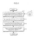
Referring now to the flowchart of Fig. 5, description is made of a fabrication
method for a semiconductor laser apparatus according to the first embodiment. In Fig. 5,
there is first acquired from a data base 30 a relationship of drive power to optical output
power for cavity length taken as a parameter (step S101), that is, the relationship shown
in Fig. 4. Thereafter, a desirable optical output power is set (step S102), and a cavity
length having minimal drive power is determined in correspondence to the set desirable
optical output power (step S103). Thereafter, a semiconductor laser apparatus that has the
determined cavity length is fabricated (step S104), before the process ends.
In the first embodiment, there described five parameters as cavity lengths of
800µm, 1000µm, 1300µm, 1500µm, and 1800µm, whereas, without limitation thereto, for
other cavity lengths also, a relationship of electric drive power to optical output power
may be determined, or interpolated, to thereby have a more detail cavity length
determined with high precision. In this case, the cavity length to be determined may not
be a cavity length corresponding to a minimum value of drive power, but may preferably
be under a cavity length for specified drive power.
Further, in the first embodiment, characteristic curves in Fig. 4 are
complemented with theoretical values on concrete empirical values, whereas their
certainty may well be enhanced by obtaining the more empirical values.
Second embodiment
Next, description is made of a second embodiment of the invention. Although,
in the first embodiment, a relationship between drive power and optical output power
shown in Fig. 4 is used to determine a cavity length to have minimal drive power for a
desirable optical output power, the second embodiment employs a relationship of
photoelectric conversion efficiency to cavity length for optical output power taken as a
parameter, to be used to determine a cavity length in correspondence to a maximal
photoelectric conversion efficiency.
As shown in Fig. 6, in determination of a relationship of photoelectric
conversion efficiency to cavity length for optical output power taken as a parameter, there
appears an optical value to have the photoelectric conversion efficiency maximal for a
respective optical output power. Therefore, by determining a cavity length corresponding
to a point where the photoelectric conversion efficiency has a maximum value for a
desirable optical output power, there can be determined a cavity length that renders the
photoelectric conversion efficiency maximal, so that a semiconductor laser apparatus
implemented with this cavity length can serve as a semiconductor laser apparatus high of
photoelectric conversion efficiency. For photoelectric conversion efficiency to be high
means for electric drive power to be minimal (i.e., high conversion efficiency implies low
electric drive power).
For example, in Fig. 6, for an optical output power of 360 mW to be obtained,
the maximum value of photoelectric conversion efficiency is 0.15, when the cavity length
is 1500µm. Therefore, by giving the cavity length of 1500µm, there can be implemented
a semiconductor laser apparatus of a 360 mW optical output power with the highest
photoelectric conversion efficiency. Further, for an optical output power of 50 mW to be
obtained, the maximum value of photoelectric conversion efficiency is 0.34, when the
cavity length is 1000µm. Therefore, by giving the cavity length of 1000µm, there can be
implemented a semiconductor laser apparatus of a 50 mW optical output power with the
highest photoelectric conversion efficiency.
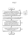
Referring now to the flowchart of Fig. 7, description is made of a fabrication
method for a semiconductor laser apparatus according to the second embodiment. In
Fig. 7, there is first acquired from a data base 30 a relationship of photoelectric
conversion efficiency to cavity length for a specified optical output power as a parameter
(step S201), that is, the relationship shown in Fig. 6. Thereafter, a desirable optical output
power is set (step S202), and a cavity length having a photoelectric conversion efficiency
as a maximal or in a vicinity of a maximum is determined in correspondence to the set
desirable optical output power (step S203). Thereafter, a semiconductor laser apparatus
that has the determined cavity length is fabricated (step S204), before the process ends.
The relationship between cavity length and optical output power for a maximal
photoelectric conversion efficiency shown in Fig. 6 may be based on to obtain an
approximation expression L1 representing a relationship between cavity length and
optical output power, to thereby determine a cavity length depending on this
approximation expression L1. In the approximation expression L1, obtained maximal
values are associated by a predetermined approximation expression. The approximation
expression L1 represents a relationship between an optical output power and an optical
cavity length, and allows for an optimal cavity length to be directly determined by
substituting a desirable value for optical output power.
Although, in the second embodiment, there is determined a cavity length to
provide a maximal photoelectric conversion efficiency, there may be determined, without
limiting thereto, a cavity length for a photoelectric conversion efficiency to be lower than
specified, or a cavity length for a photoelectric conversion efficiency to be in a vicinity of
a maximum. The vicinity of the maximum may cover cavity lengths within a range
specified by a given percentage that corresponds to a photoelectric conversion efficiency
of the maximum value, or cavity lengths within a range specified by a given percentage
relative to a reference as a cavity length corresponding to a photoelectric conversion
efficiency of the maximum value. There may be provided a specified margin for a cavity
length determined by the approximation expression L1, as the margin corresponds to a
range of the vicinity of maximum. For photoelectric conversion efficiency, the
percentage is preferably 10%, and more preferably 6%, and most preferably 3%. For
cavity length, the percentage is preferably 40%, and more preferably 20%, and most
preferably 10%.
Third embodiment
Next, description is made a third embodiment of the invention. Although, in the
second embodiment, a relationship of photoelectric conversion efficiency to cavity length
for optical output power taken as a parameter is based on to determine a cavity length to
have maximal photoelectric conversion efficiency for a desirable optical output power,
the third embodiment employs a relationship of electric drive power to cavity length for
optical output power taken as a parameter, to be based on to determine a cavity length to
have minimal drive power for a desirable optical output power to be obtained. That is,
the photoelectric conversion efficiency in the second embodiment is rendered to be
substantially identical drive power.
Fig. 8 is a graph showing a relationship of electric drive power to a cavity length
for optical output power taken as a parameter. In Fig. 8, contrary to the photoelectric
conversion efficiency in Fig. 6, electric drive power stands as a characteristic having a
minimum value. In Fig. 8, for a respective optical output power, there is a corresponding
cavity length for the drive power to have a minimum value. In particular, as the optical
output power increases, the minimum value appears more significant. For example, for
an optical output power of 360 mW, the minimum value of drive power is 2.4 W, when
the cavity length is 1500µm. Like this, for a desirable optical output power, there can be
determined a cavity length that minimizes the drive power.
Referring now to the flowchart of Fig. 9, description is made of a fabrication
method for a semiconductor laser apparatus according to the third embodiment. In Fig. 9,
there is first acquired from a data base 30 a relationship of electric drive power to cavity
length for a specified optical output power as a parameter (step S301), that is, the
relationship shown in Fig. 8. Thereafter, a desirable optical output power is set (step
S302), and a cavity length having drive power as a minimal or in a vicinity of a minimum
is determined in correspondence to the set desirable optical output power (step S303).
Thereafter, a semiconductor laser apparatus that has the determined cavity length is
fabricated (step S304), before the process ends.
The relationship between cavity length and optical output power for minimal
drive power shown in Fig. 8 may be based on to obtain an approximation expression L2
representing a relationship between cavity length and optical output power, to thereby
determine a cavity length depending on this approximation expression L2. In the
approximation expression L2, obtained minimal values are associated by a predetermined
approximation expression. The approximation expression L2 represents a relationship
between an optical output power and an optical cavity length, and allows for an optimal
cavity length to be directly determined by substituting a desirable value for optical output
power.
Although, in the third embodiment, there is determined a cavity length to render
drive power minimal, there may be determined, without limiting thereto, a cavity length
for drive power to be lower than specified, or a cavity length for drive power to be in a
vicinity of a minimum. The vicinity of the minimum may cover cavity lengths within a
range specified by a given percentage that corresponds to drive power of the minimum
value, or cavity lengths within a range specified by a given percentage relative to a
reference as a cavity length corresponding to drive power of the maximum value. There
may be provided a specified margin for a cavity length determined by the approximation
expression L2, as the margin corresponds to a range of the vicinity of minimum. For drive
power, the percentage is preferably 10%, and more preferably 6%, and most preferably
3%. For cavity length, the percentage is preferably 40%, and more preferably 20%, and
most preferably 10%.
Although, in the foregoing first to third embodiments, the cavity length is
described as 1800µm at maximum, there may be employed, without limiting thereto, yet
longer cavity lengths, as well, to be likewise applied. In particular, when an increased
optical output power is desirable, there is required a yet longer cavity length, whereby the
semiconductor laser apparatus 20 has increased drive power, with the more enhanced
functions and effects to be exhibited in this embodiment.
Fourth embodiment
Next, description is made a fourth embodiment of the invention. Although, in
the foregoing first to third embodiments, there is a cavity length to have minimal electric
drive power or maximal photoelectric conversion efficiency for a desirable optical output
power, the fourth embodiment is configured to determine, from a desirable optical output
power and a specified cavity length, a hole carrier concentration of an upper cladding
layer (p-InP cladding layer 6) to have minimal electric drive power.
Fig. 10 is a graph showing a relationship of electric drive power to a hole carrier
concentration in the upper cladding layer for specified optical output power and specified
cavity length taken as parameters. In Fig. 10, for a respective combination of a specified
cavity length of 800µm or 1000µm and a specified optical output power such as 150 mW,
170 mW, or 190 mW, there is a corresponding hole carrier concentration in the upper
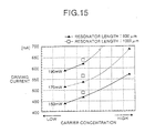
cladding layer for the drive power to be minimal. Incidentally, as shown in Fig. 15, if a
relationship is determined between an driving current and the hole carrier concentration in
the upper cladding layer for a specified optical output power and a specified cavity length
as parameters, the relationship has a monotonically increasing driving current, as the hole
carrier concentration becomes higher, giving no optimum value. In other words, the hole
carrier concentration has a minimum value, from view point of drive power.
It therefore is allowed to determine a hole carrier concentration in the upper
cladding layer that minimizes the driving current relative to a desirable optical output
power and a specified cavity length. With cavity length the more optimized, the more the
driving current can be reduced, like the first to third embodiments.
For example, if the desirable optical output power is 190 mW and the cavity
length is 800µm, then the hole carrier concentration in the upper cladding layer takes a
value Cz to have minimal drive power, that is 1.2 W. This driving current becomes 1.1 W,
by setting the cavity length to 1000µm.
Referring now to the flowchart of Fig. 11, description is made of a fabrication
method for a semiconductor laser apparatus according to the fourth embodiment. In
Fig. 11, there is first acquired from a data base 30 a relationship of electric drive power to
hole carrier concentration in the upper cladding layer for a specified optical output power
and a specified cavity length as parameters (step S401), that is, the relationship shown in
Fig. 10. Thereafter, a desirable optical output power and a specified cavity length are set
(step S402), and a hole carrier concentration having drive power as a minimal or in a
vicinity of a minimum is determined in correspondence to the set desirable optical output
power and specified cavity length (step S403). Thereafter, a semiconductor laser
apparatus that has the determined hole carrier concentration is fabricated (step S404),
before the process ends.
The relationship between optical output power and hole carrier concentration for
minimal drive power shown in Fig. 8 may be based on to obtain an approximation
expression representing a relationship between hole carrier concentration and
combination of optical output power and cavity length, to thereby determine a carrier
concentration depending on this approximation expression. In the approximation
expression, obtained minimal values are associated by a predetermined approximation
expression. The approximation expression represents a relationship between an optimal
hole carrier concentration and combination of optical output power and cavity length, and
allows for an optimal hole carrier concentration to be directly determined by substituting
a desirable value for optical output power and a specified value for cavity length.
Although, in the fourth embodiment, there is determined an optimal hole
concentration due to Zn doping based on a relationship of drive power to hole carrier
concentration, there may be determined, without limiting thereto and like the second
embodiment, a relationship of photoelectric conversion efficiency to hole carrier
concentration for specified optical output power and specified cavity length as
parameters, to thereby determine a hole carrier concentration that maximizes the
photoelectric conversion efficiency.
Further, although, in the fourth embodiment, there is determined a hole carrier
concentration to render drive power minimal, there may be determined, without limiting
thereto, a hole carrier concentration for drive power to be lower than specified, or a hole
carrier concentration for drive power to be in a vicinity of a minimum. The vicinity of the
minimum may cover hole carrier concentrations within a range specified by a given
percentage that corresponds to drive power of the minimum value, or hole carrier
concentrations within a range specified by a given percentage relative to a reference as a
hole carrier concentration corresponding to drive power of the maximum value. There
may be provided a specified margin for a hole carrier concentration determined by the
approximation expression, as the margin corresponds to a range of the vicinity of
minimum.
Although, in the foregoing first to fourth embodiments, the cavity length or hole
carrier concentration in an upper cladding layer of semiconductor laser apparatus 20 is
determined to render the drive power minimal or vicinal to a minimum or the
photoelectric conversion efficiency maximal or vicinal to a maximum, there may be
likewise determined, without limiting thereto, respective elements of the semiconductor
laser apparatus 20. For example, there may be determined a value of reflection factor of
the reflective film 14 or projection side reflective film 15 of the semiconductor laser
apparatus 20.
Fifth embodiment
Next, description is made a fifth embodiment of the invention. In the fifth
embodiment, a semiconductor laser apparatus according to any of the first to fourth
embodiments is made as a module.
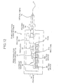
Fig. 12 is a longitudinal sectional view showing an arrangement of a
semiconductor laser module according to the fifth embodiment. In Fig. 12, this
semiconductor laser module 50 has a semiconductor laser module 51 corresponding to
any of the semiconductor laser modules in the first to fourth embodiments. On an inner
bottom of a package 59 formed by a ceramic or the like as a housing of the semiconductor
laser module 50, there is disposed a Peltier device 58 as a temperature controller. The
Peltier device 58 has a base 57 disposed thereon, and a heat sink 57a disposed on the base
57a.
On the base 57 is disposed the semiconductor laser apparatus 51, as well as the
heat sink 57a provided with a thermistor 58a, a first lens 52, and an electric current
monitor 56. Laser light projected from the semiconductor laser apparatus 51 is conducted
via the first lens 52, an isolator 53, and a second lens 54, to an optical fiber 55. The
second lens 54 is installed on an optical axis of the laser light, on the package 59, to be
optically coupled with the optical fiber 55 for external connection. The electric current
monitor 56 monitors (i.e., detects for) leaked light at the reflection film end of the
semiconductor laser apparatus 51.
The isolator 53 is interposed between the semiconductor laser apparatus 52 and
the optical fiber 55, to prevent reflection return light, such as from other optics, from reentering
the cavity.
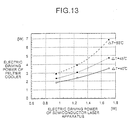
Fig. 13 is a graph showing a relationship between electric drive power of the
semiconductor laser apparatus 51 and electric drive power of the Peltier device 58 in the
case a temperature difference between a temperature of the semiconductor laser apparatus
51 and an ambient temperature is taken as a parameter. The drive power supplied to the
Peltier device 58 is varied in dependence on the temperature difference ΔT between the
temperature of the semiconductor laser apparatus 51 and the ambient temperature. As
shown in Fig. 13, the larger the temperature difference ΔT becomes, the greater the drive
power to be applied to the Peltier device 58 becomes. For example, for the
semiconductor laser apparatus 51 to be kept at a temperature of 25°C against an ambient
temperature of 75°C, it is necessary to set the temperature difference ΔT to 50°C. In this
case, if the drive power of the semiconductor laser apparatus 20 is 1.7 W, then the drive
power to be applied to the Peltier device 58 is 7 W.
In this respect, by applying the semiconductor laser apparatus 20 of any of the
first to fourth embodiments to the semiconductor laser module 50, the drive power to be
applied to the Peltier device 58 can be reduced, as the drive power of the semiconductor
laser device 20 is made small. For example, in the case the temperature difference ΔT to
be kept is 50°C, if the drive power of the semiconductor laser device 20 is reduced from
1.7 W to 1.25 W, then the drive power to be applied to the Peltier device 58 decreases
from 7 W to 4 W, thus achieving a reduction of power consumption by an amount of 3 W
in addition to a power consumption reduction at the semiconductor laser apparatus 20.
Like this, promotion of power consumption reduction of the semiconductor laser
apparatus 20 itself leads to a reduction in the power consumption reduction of the entire
semiconductor laser module 50.
Although, in the fifth embodiment, the semiconductor laser module is of a type
in which laser light output from the semiconductor laser apparatus 20 is directly output,
the invention may well be applied to a semiconductor laser module having an optical fiber
grating of such a type that an optical fiber grating is formed in a vicinity of a second lens
54 side end of the optical fiber 55, and laser light output from the semiconductor laser
apparatus 51 is output after a wavelength selection by the optical fiber grating.
In the fifth embodiment, a semiconductor laser apparatus according to any of the
first to fourth embodiments is made as a module having a reduced power consumption, in
particular at the Peltier device 58, with a resultant reduction of the total drive power of
the entire semiconductor laser module 50, allowing for an enhanced photoelectric
conversion efficiency.
As explained above, according to the first aspect of the invention, by
implementation of a semiconductor laser apparatus wherein a respective element value of
the semiconductor laser apparatus is determined on the basis of relationships between
respective elements of the semiconductor laser apparatus including a cavity length of the
semiconductor laser apparatus and a carrier concentration of an upper cladding layer of
the semiconductor laser apparatus and a photoelectric conversion efficiency or an electric
drive power of the semiconductor laser apparatus, for optical output power to be constant
as a parameter, so that the electric drive power is vicinal to a minimum thereof or the
photoelectric conversion efficiency is vicinal to a maximum thereof in correspondence to
a desirable optical output power, it is enabled to obtain an desirable optical output power
in a range over 50 mW, with a photoelectric conversion efficiency in a vicinity of a
maximum or an electric drive power in a vicinity of a minimum. Consequently, a
semiconductor laser apparatus that is capable of obtaining a desirable optical output
power either at the electric drive power is vicinal to a minimum or the electric drive
power is vicinal to a maximum is achieved easily. Further, As the photoelectric
conversion efficiency becomes vicinal to a maximum, a reactive power is restrained, and
temperature increase of the active layer of the semiconductor laser apparatus is restrained,
thus the dependability of the semiconductor laser apparatus is improved.
According to the second aspect of the invention, by implementation of a
semiconductor laser apparatus wherein a cavity length over 1000 µm is determined on the
basis of a relationship of an electric drive power to a range of optical output power over
50 mW, for cavity length to be constant as a parameter in a range over 1000 µm, so that
the electric drive power is vicinal to a minimum thereof in correspondence to a desirable
optical output power, it is enabled to obtain an desirable optical output power in a range
over 50 mW, with an electric drive power in a vicinity of a minimum. Consequently, a
semiconductor laser apparatus that is capable of obtaining a desirable optical output
power at the electric drive power is vicinal to a minimum is achieved easily. Further, As
the drive power becomes vicinal to a minimum, a reactive power is restrained, and
temperature increase of the active layer of the semiconductor laser apparatus is restrained,
thus the dependability of the semiconductor laser apparatus is improved.
According to the third aspect of the invention, by implementation of a
semiconductor laser apparatus wherein a cavity length is determined on the basis of a
relationship of a photoelectric conversion efficiency to a range of cavity length over
1000 µm, for optical output power to be constant as a parameter in a range over 50 mW,
so that the photoelectric conversion efficiency is vicinal to a maximum thereof in
correspondence to a desirable optical output power. Consequently, it is enabled to easily
obtain a semiconductor laser apparatus with a desirable optical output power with high
photoelectric conversion efficiency.
According to the fourth aspect of the invention, determination of the cavity
length is based an approximation expression making the photoelectric conversion
efficiency maximal in correspondence to the desirable optical output power.
Consequently, with using computers, it is enabled to quickly determine a cavity length of
a semiconductor laser apparatus by a desirable optical output power with high
photoelectric conversion efficiency.
According to the fifth aspect of the invention, by implementation of a
semiconductor laser apparatus having a cavity length over 1000 µm determined on the
basis of a relationship of an electric drive power to a range of cavity length over 1000 µm,
for optical output power to be constant as a parameter in a range over 50 mW, so that the
electric drive power is vicinal to a minimum thereof in correspondence to a desirable
optical output power, it is enabled to obtain an desirable optical output power in a range
over 50 mW, with a low electric drive power. Consequently, it is enabled to easily obtain
a semiconductor laser apparatus with a desirable optical output power with a low drive
power.
According to the sixth aspect of the invention, when the cavity length is
determined, it is determined on the basis of an approximation expression making an
electric drive power minimal in correspondence to the desirable optical output power.
Consequently, with using computer programs or the like, it is enabled to quickly
determine a cavity length of a cavity length of a semiconductor laser apparatus by a
desirable optical output power with a low drive power.
According to the seventh aspect of the invention, as an active layer forming a
cavity with the cavity length, there is applied a strain multiple quantum well structure,
while it is enabled even for the semiconductor laser apparatus having a strain multiple
quantum well structure to obtain an desirable optical output power in a range over
50 mW, with high photoelectric conversion efficiency or a low electric drive power.
Consequently, it is enabled to obtain a high flexibility that can be applied to a
semiconductor laser apparatus having various structures.
According to the eighth aspect of the invention, there is implemented a concrete
semiconductor laser apparatus to be distinctive, particularly when letting the desirable
optical output power be within a range of 50 mW to 400 mW and the cavity length be
within a range of 1000 µm to 1600 µm, and determining the cavity length simply from the
relationship of the electric drive power to the optical output power. Consequently, it is
enabled to obtain a desirable optical output power with a high photoelectric power
conversion efficiency or a low electric drive power.
According to the ninth aspect of the invention, there is implemented a concrete
semiconductor laser apparatus to be distinctive, particularly when letting the desirable
optical output power be within a range of 50 mW to 200 mW and the cavity length be
within a range of 1000 µm to 1400 µm, and determining the cavity length simply from the
relationship of the electric drive power to the optical output power. Consequently, it is
enabled to obtain a desirable optical output power with a high photoelectric power
conversion efficiency or low electric drive power.
According to the tenth aspect of the invention, by implementation of a
semiconductor laser apparatus, an upper cladding layer has an impurity carrier
concentration determined on the basis of a relationship of a photoelectric conversion
efficiency or an electric drive power to the impurity carrier concentration of the upper
cladding layer, for optical output power and cavity length to be constant as parameters, so
that the electric drive power is vicinal to a minimum thereof or the photoelectric
conversion efficiency is vicinal to a maximum thereof in correspondence to a desirable
optical output power, it is enabled to obtain an desirable optical output power in a range
over 50 mW, with a photoelectric conversion efficiency in a vicinity of a maximum or an
electric drive power in a vicinity of a minimum. Consequently, it is enabled to easily
obtain a semiconductor laser apparatus that is capable of obtaining a desirable optical
output power at the electric drive power is vicinal to a minimum and the photoelectric
conversion efficiency is vicinal to a maximum.
According to the eleventh aspect of the invention, by implementation of a
semiconductor laser module with an incorporated semiconductor laser apparatus
according to any of the first to tenth aspects of the invention, it is enabled to achieve an
desirable optical output power, with high photoelectric conversion efficiency or a low
electric drive power. Consequently, with the semiconductor laser module on the whole, it
is enabled to obtain a desirable optical output power with a high photoelectric power
conversion efficiency or a low electric drive power.
According to the twelfth aspect of the invention, an optical fiber grating is
formed in a vicinity of an incidence end of the optical fiber, and laser light of a
wavelength selected by the optical fiber grating is output. Consequently, even with the
semiconductor laser module to achieve the semiconductor laser apparatus using an optical
fiber grating, it is enabled to obtain a desirable optical output power with a high
photoelectric power conversion efficiency or a low electric drive power.
According to the thirteenth aspect of the invention, by implementation of a
semiconductor laser module with an incorporated semiconductor laser apparatus
according to any of the first to tenth aspects of the invention, it is enabled even for the
semiconductor laser module with an incorporated temperature controller to obtain an
desirable optical output power, with high photoelectric conversion efficiency or a low
electric drive power. Consequently, with the semiconductor laser module on the whole, it
is enabled to obtain a desirable optical output power with a high photoelectric power
conversion efficiency or a low electric drive power.
According to the fourteenth aspect of the invention, for fabrication of a
semiconductor laser apparatus, in a relationship acquiring step there are acquired
relationships between respective elements of the semiconductor laser apparatus including
a cavity length of the semiconductor laser apparatus and a carrier concentration of an
upper cladding layer of the semiconductor laser apparatus and a photoelectric conversion
efficiency or an electric drive power of the semiconductor laser apparatus, for optical
output power to be constant as a parameter, in an element value determining step there is
determined a respective element value of the semiconductor laser apparatus to be
determined on the basis of the relationships acquired by the relationship acquiring step, so
that the electric drive power is vicinal to a minimum thereof or the photoelectric
conversion efficiency is vicinal to a maximum thereof in correspondence to a desirable
optical output power, and in a forming step there is formed the semiconductor laser
apparatus having the respective element value determined by the element value
determining step. Consequently, it is enabled to easily manufacture a semiconductor laser
apparatus that is capable of obtaining a desirable optical output power at the electric drive
power is vicinal to a minimum and the photoelectric conversion efficiency is vicinal to a
maximum.
According to the fifteenth aspect of the invention, for fabrication of a
semiconductor laser apparatus, in a relationship acquiring step there is acquired a
relationship of an electric drive power to a range of optical output power over 50 mW, for
cavity length to be constant as a parameter in a range over 1000 µm, in a cavity length
determining step there is determined a cavity length over 1000 µm to be determined on
the basis of the relationship acquired by the relationship acquiring step, so that the electric
drive power is vicinal to a minimum thereof in correspondence to a desirable optical
output power, and in a forming step there is formed the semiconductor laser apparatus
having the cavity length determined by the cavity length determining step. Consequently,
it is enabled to easily obtain a semiconductor laser apparatus that is capable of obtaining a
desirable optical output power at the electric drive power is vicinal to a minimum.
According to the sixteenth aspect of the invention, for fabrication of a
semiconductor laser apparatus, in a relationship acquiring step there is acquired a
relationship of a photoelectric conversion efficiency to a range of cavity length over 1000
µm, for optical output power to be constant as a parameter in a range over 50 mW, in a
cavity length determining step there is determined a cavity length to be determined on the
basis of the relationship acquired by the relationship acquiring step, so that the
photoelectric conversion efficiency is vicinal to a maximum thereof in correspondence to
a desirable optical output power, and in a forming step there is formed the semiconductor
laser apparatus having the cavity length determined by the cavity length determining step.
Consequently, it is enabled to easily obtain a semiconductor laser apparatus that is
capable of obtaining a desirable optical output power with a high photoelectric conversion
efficiency.
According to the seventeenth aspect of the invention, an approximation
expression calculating step determines an approximation expression for making the
photoelectric conversion efficiency maximal in correspondence to the desirable optical
output power, on the basis of the relationship acquired by the relationship acquiring step,
and the cavity length determining step determines the cavity length on the basis of the
approximation expression. Consequently, with using computer programs or the like, it is
enabled to quickly determine a cavity length of a cavity length of a semiconductor laser
apparatus obtainable by a desirable optical output power with a high photoelectric
conversion efficiency.
According to the eighteenth aspect of the invention, for fabrication of a
semiconductor laser apparatus, in a relationship acquiring step there is acquired a
relationship of an electric drive power to a range of cavity length over 1000 µm, for
optical output power to be constant as a parameter in a range over 50 mW, in a cavity
length determining step there is determined a cavity length over 1000 µm to be
determined on the basis of the relationship acquired by the relationship acquiring step, so
that the electric drive power is vicinal to a minimum thereof in correspondence to a
desirable optical output power, and in a forming step there is formed the semiconductor
laser apparatus having the cavity length determined by the cavity length determining step.
Consequently, it is enabled to quickly determine a cavity length of a cavity length of a
semiconductor laser apparatus with a desirable optical output power with a low drive
power.
According to the nineteenth aspect of the invention, an approximation expression
calculating step determines an approximation expression for making the electric drive
power minimal in correspondence to the desirable optical output power, on the basis of
the relationship acquired by the relationship acquiring step, and the cavity length
determining step determines the cavity length on the basis of the approximation
expression. Consequently, with using computer programs or the like, it is enabled to
quickly determine a cavity length of a cavity length of a semiconductor laser apparatus
obtainable by a desirable optical output power with a low drive power.
According to the twentieth aspect of the invention, as an active layer forming a
cavity with the cavity length there is applied a strain multiple quantum well structure,
while it is enabled even for the semiconductor laser apparatus having a strain multiple
quantum well structure to obtain an desirable optical output power in a range over 50
mW, with high photoelectric conversion efficiency or a low electric drive power.
Consequently, it is enabled to obtain a high flexibility that can be applied to a
semiconductor laser apparatus having various structures.
According to the twenty-first aspect of the invention, for fabrication of a
semiconductor laser apparatus, in a relationship acquiring step there is acquired a
relationship of an electric drive power to an impurity carrier concentration of an upper
cladding layer, for optical output power and cavity length to be constant as parameters, in
a carrier concentration determining step there is determined the impurity carrier
concentration to be determined on the basis of the relationship acquired by the
relationship acquiring step, so that the electric drive power is vicinal to a minimum
thereof in correspondence to a desirable optical output power, and in a forming step there
is formed the semiconductor laser apparatus with the upper cladding layer having the
impurity carrier concentration thereof set to the impurity carrier concentration determined
by the carrier concentration determining step. Consequently, it is enabled to easily obtain
a semiconductor laser apparatus that is capable of obtaining a desirable optical output
power at the electric drive power is vicinal to a minimum and the photoelectric
conversion efficiency is vicinal to a maximum.
Having thus generally described the aspects of the present invention, we now
describe the results of the application of the present invention to the specific area of
Group III-V semiconductor lasers having the following general features:
- A resonator cavity having a front facet, a back facet, and a length L between
facets in the range of approximately 1000 µm to approximately 1800 µm,
- an active layer disposed within the resonator cavity and being electrically
coupled to two electrodes for receiving an electrical bias potential,
- a low reflectance coating disposed on the front facet having a reflectivity of
less than approximately 4%,
- a high reflectance coating disposed on the back facet and having a
reflectivity of more than approximately 80%, and
- a hole carrier concentration in the upper cladding layer above the active
layer, with a value in the range of 4x1017 cm-3 to 1x1018 cm-3 (with 7x10¹⁷
cm-3 being exemplary), preferably provided by Zn (zinc) doping.
Group III-V semiconductors comprise one or more of the following compounds
formed as layer structures: GaAs, InGaAs, AlGaAs, InGaAsP, InP.
FIG. 16 shows the ranges of cavity length L of this category of
semiconductor lasers which results in an input electrical drive power that is within
approximately 5% to approximately 10% of the minimum drive power for a given
value of optical output power P
OUT in the range between 50 mW and 390 mW, and/or
which results in a photoelectric conversion efficiency that is within approximately
5% to approximately 10% of the maximum conversion efficiency for the given value
of P
OUT. (The region of cavity length less than 1000 µm was omitted in order to
satisfy the requirement from the maximum rating.) The exterior vertices of the area
of ranges is defined by the following 12 points P1-P12, which are shown in FIG. 16
and have the following values:
| Point | Length Value | Power value |
| P1 | 1380 µm | 50 mW |
| P2 | 1480 µm | 100 mW |
| P3 | 1700µm | 200 mW |
| P4 | 1750 µm | 300 mW |
| P5 | 1750 µm | 360 mW |
| P6 | 1770 µm | 390 mW |
| P7 | 1450 µm | 390 mW |
| P8 | 1350 µm | 360 mW |
| P9 |
| | 1200 µm | 300 mW |
| P10 | 1050 µm | 200 mW |
| P11 |
| | 1000 µm | 100 mW |
| P12 | 1000 µm | 50 mW |
A plurality of line segments 540-551 connect points P1-P12 and define the outer
edges of the range area. Line segments 547-551 define the lower bounds (left side)
of cavity lengths, and line segments 541-545 define the upper bounds (right side) of
cavity lengths. FIG. 16 may also be viewed as providing preferred operating ranges
for the optical output power for a given cavity length of the laser. In this case,
segment 540-545 define the lower bounds (bottom side) of optical output powers, and
segments 546-551 define the upper bounds (top side) of the optical output powers.
The line segments 540-551 shown in FIG. 16 may be mathematically defined
by the following sets of equations, each capable of being defined as a function of
cavity length L or as a function of output power P
OUT:
| Line Segment 540 |
| Span over L: 1000 µm to 1380 µm |
| Span over POUT: 50 mW to 50 mW |
| L = [1000 µm, 1380 µm] | (1A) |
| POUT = 50 mW | (1B) |
| Line Segment 541 |
| Span over L: 1380 µm to 1480 µm |
| Span over POUT: 50 mW to 100 mW |
| L = (100µm/50mW)*POUT + 1280 µm | (2A) |
| = 2µm*(POUT/1mW) +1280 µm | (2B) |
| POUT = (1mW)*[(L-1280 µm)/2µm)] | (2C) |
| Line Segment 542 |
| Span over L: 1480 µm to 1700 µm |
| Span over POUT: 100 mW to 200 mW |
| L = (220µm/100mW)*POUT + 1260 µm | (3A) |
| = 2.2µm*(POUT/1mW) +1260 µm | (3B) |
| POUT = (1mW)*[(L-1260 µm)/2.2µm)] | (3C) |
| Line Segment 543 |
| Span over L: 1700 µm to 1750 µm |
| Span over POUT: 200 mW to 300 mW |
| L = (50µm/100mW)*POUT + 1600 µm | (4A) |
| = 1µm*(POUT/2mW) +1600 µm | (4B) |
| POUT = (2mW)*[(L-1600 µm)/1µm)] | (4C) |
| Line Segment 544 |
| Span over L: 1750 µm to 1750µm |
| Span over POUT: 300 mW to 360 mW |
| L = 1750 µm | (5A) |
| POUT = [300 mW, 360 mW] | (5B) |
| Line Segment 545 |
| Span over L: 1750 µm to 1770 µm |
| Span over POUT: 360 mW to 390 mW |
| L = (20µm/30mW)*POUT + 1510 µm | (6A) |
| = 2µm*(POUT/3mW) +1510 µm | (6B) |
| POUT = (3mW)*[(L-1510 µm)/2µm)] | (6C) |
| Line Segment 546 |
| Span over L: 1450 µm to 1770 µm |
| Span over POUT: 390 mW to 390 mW |
| L = [1450 µm, 1770 µm] | (7A) |
| POUT = 390 mW | (7B) |
| Line Segment 547 |
| Span over L: 1350 µm to 1450 µm |
| Span over POUT: 360 mW to 390 mW |
| L = (100µm/30mW)*POUT + 150 µm | (8A) |
| = 10µm*(POUT/3mW) +150 µm | (8B) |
| POUT = (3mW)*[(L-150 µm)/10µm)] | (8C) |
| Line Segment 548 |
| Span over L: 1200 µm to 1350 µm |
| Span over POUT: 300 mW to 360 mW |
| L = (150µm/60mW)*POUT + 450 µm | (9A) |
| = 5µm*(POUT/2mW) +450 µm | (9B) |
| POUT = (2mW)*[(L-450 µm)/5µm)] | (9C) |
| Line Segment 549 |
| Span over L: 1050 µm to 1200 µm |
| Span over POUT: 200 mW to 300 mW |
| L = (150µm/100mW)*POUT + 750 µm | (10A) |
| = 3µm*(POUT/2mW) +750 µm | (10B) |
| POUT = (2mW)*[(L-750 µm)/3µm)] | (10C) |
| Line Segment 550 |
| Span over L: 1000 µm to 1050 µm |
| Span over POUT: 100 mW to 200 mW |
| L = (50µm/100mW)*POUT + 950 µm | (11A) |
| = 1µm*(POUT/2mW) + 950 µm | (11B) |
| POUT = (2mW)*[(L-950 µm)/1µm)] | (11C) |
| Line Segment 551 |
| Span over L: 1000 µm to 1000 µm |
| Span over POUT: 50 mW to 100 mW |
| L = 1000 µm | (12A) |
| POUT = [50 mW, 100 mW] | (12B) |
The ranges encompass the six measurement data sets shown in FIGS. 6 and 8 taken at
output powers P
OUT of 50mW, 100mW, 200mW, 300mW, 360mW, and 390 mW,
which are indicated in FIG. 16 as lines 501-506.
With lines segments 540-551, the span of desired cavity length L may be
divided into the nine ranges indicated in Table II, where "~" means "approximately."
The values of P
OUT within these ranges are bounded by the line and data segments
indicated in Table II.
| L Range | Line Segment Lower Bound For POUT | Line Segment Upper Bound For POUT |
| ∼1000 µm to ∼1050 µm | Line Segment 540 | Line Segment 550 |
| | (equation 1B, 50 mW) | (equation 11C) |
| ∼1050 µm to ∼1200 µm | Line Segment 540 | Line Segment 549 |
| | (equation 1B, 50 mW) | (equation 10C) |
| ∼1200 µm to ∼1350 µm | Line Segment 540 | Line Segment 548 |
| | (equation 1B, 50 mW) | (equation 9C) |
| ∼1350 µm to ∼1380 µm | Line Segment 540 | Line Segment 547 |
| | (equation 1B, 50 mW) | (equation 8C) |
| ∼1380 µm to ∼1450 µm | Line Segment 541 | Line Segment 547 |
| | (equation 2C) | (equation 8C) |
| ∼1450 µm to ∼1480 µm | Line Segment 541 | Line Segment 546 |
| | (equation 2C) | (equation 7B, 390 mW) |
| ∼1480 µm to ∼1700 µm | Line Segment 542 | Line Segment 546 |
| | (equation 3C) | (equation 7B, 390 mW) |
| ∼1700 µm to ∼1750 µm | Line Segment 543 | Line Segment 546 |
| | (equation 4C) | (equation 7B, 390 mW) |
| ∼1750 µm to ∼1770 µm | Line Segment 545 | Line Segment 546 |
| | (equation 6C) | (equation 7B, 390 mW) |
Given a laser with a specific length, one may locate the corresponding range for the
given length, and then operate the laser at a power level that is at or between the
lower and upper bounds specified for the length's range. Such operation can be
readily achieved with a power supply (see FIG. 1) which is coupled to the laser's
power electrodes and which is configured to apply an amount of power which causes
the semiconductor laser to operate with the selected optical output power. The
present invention encompasses a laser device operated in this manner, as well as a
method of operating a laser in this manner by selecting an operating optical output
power based on the laser's length in accordance with FIG. 16 and Table II.
In a similar manner, the span of optical output power P
OUT may be divided
into five ranges, as provided in Table III. The values of cavity length L within these
ranges are bounded by the line and data segments indicated in Table II.
| POUT Range | Lower Bound For L | Upper Bound For L |
| ∼50mW to ∼100mW | Line Segment | 551 | Line Segment 541 |
| | (equation 12A, L=1000µm) | (equation 2A or 2B) |
| ∼100mW to ∼200mW | Line Segment | 550 | Line Segment 542 |
| | (equation 11A or 11B) | (equation 3A or 3B) |
| ∼200mW to ∼300mW | Line Segment 549 | Line Segment 543 |
| | (equation 10A or 10B) | (equation 4A or 4B) |
| ∼300mW to ∼360mW | Line Segment | 548 | Line Segment 544 |
| | (equation 9A or 9B) | (equation 5A, L=1750µm) |
| ∼360mW to ∼390mW | Line Segment | 547 | Line Segment 545 |
| | (equation 8A or 8B) | (equation 6A or 6B) |
Given a specific optical output power level for a laser, one may locate the
corresponding range for the specified power level, and then select a length for the
laser which is at or between the lower and upper bounds specified for the power
level's range. Such selection of length can be achieved by cleaving facets of the
laser chip at locations which achieve the desire length. The present invention
accordingly further encompasses a method of selecting the cavity length of a
semiconductor laser depending upon the desire optical power level in this manner, as
based upon FIG. 16 and Table III.
As described above, one may consult Table II and choose an operating power
level based upon a given cavity length. While being more complex, one may also
perform such a selection process based on Table III, in which case one examines the
second and third columns to find one or more optical output power ranges which
include the given cavity length. From the ranges found, one can then select
corresponding ranges of output power levels for the given cavity length.
It may be appreciated that the above method and laser embodiments of the
present invention may be practiced using just one of the ranges provided in Tables II
and III, or using a combination of two or more of the ranges in these tables.
The above method and laser embodiments of the present invention may also
be practiced within the following three preferred zones of FIG. 16:
Although the invention has been described with respect to specific embodiments
for a complete and clear disclosure, the appended claims are not to be thus limited but are
to be construed as embodying all modifications and alternative constructions that may
occur to one skilled in the art which fairly fall within the basic teaching herein set forth.