EP1215311A2 - Manufacturing method of silicon carbide single crystals - Google Patents
Manufacturing method of silicon carbide single crystals Download PDFInfo
- Publication number
- EP1215311A2 EP1215311A2 EP01129641A EP01129641A EP1215311A2 EP 1215311 A2 EP1215311 A2 EP 1215311A2 EP 01129641 A EP01129641 A EP 01129641A EP 01129641 A EP01129641 A EP 01129641A EP 1215311 A2 EP1215311 A2 EP 1215311A2
- Authority
- EP
- European Patent Office
- Prior art keywords
- substrate
- silicon carbide
- micro
- pipe
- front surface
- Prior art date
- Legal status (The legal status is an assumption and is not a legal conclusion. Google has not performed a legal analysis and makes no representation as to the accuracy of the status listed.)
- Granted
Links
Images




Classifications
-
- C—CHEMISTRY; METALLURGY
- C30—CRYSTAL GROWTH
- C30B—SINGLE-CRYSTAL GROWTH; UNIDIRECTIONAL SOLIDIFICATION OF EUTECTIC MATERIAL OR UNIDIRECTIONAL DEMIXING OF EUTECTOID MATERIAL; REFINING BY ZONE-MELTING OF MATERIAL; PRODUCTION OF A HOMOGENEOUS POLYCRYSTALLINE MATERIAL WITH DEFINED STRUCTURE; SINGLE CRYSTALS OR HOMOGENEOUS POLYCRYSTALLINE MATERIAL WITH DEFINED STRUCTURE; AFTER-TREATMENT OF SINGLE CRYSTALS OR A HOMOGENEOUS POLYCRYSTALLINE MATERIAL WITH DEFINED STRUCTURE; APPARATUS THEREFOR
- C30B25/00—Single-crystal growth by chemical reaction of reactive gases, e.g. chemical vapour-deposition growth
- C30B25/02—Epitaxial-layer growth
-
- C—CHEMISTRY; METALLURGY
- C30—CRYSTAL GROWTH
- C30B—SINGLE-CRYSTAL GROWTH; UNIDIRECTIONAL SOLIDIFICATION OF EUTECTIC MATERIAL OR UNIDIRECTIONAL DEMIXING OF EUTECTOID MATERIAL; REFINING BY ZONE-MELTING OF MATERIAL; PRODUCTION OF A HOMOGENEOUS POLYCRYSTALLINE MATERIAL WITH DEFINED STRUCTURE; SINGLE CRYSTALS OR HOMOGENEOUS POLYCRYSTALLINE MATERIAL WITH DEFINED STRUCTURE; AFTER-TREATMENT OF SINGLE CRYSTALS OR A HOMOGENEOUS POLYCRYSTALLINE MATERIAL WITH DEFINED STRUCTURE; APPARATUS THEREFOR
- C30B29/00—Single crystals or homogeneous polycrystalline material with defined structure characterised by the material or by their shape
- C30B29/10—Inorganic compounds or compositions
- C30B29/36—Carbides
-
- Y—GENERAL TAGGING OF NEW TECHNOLOGICAL DEVELOPMENTS; GENERAL TAGGING OF CROSS-SECTIONAL TECHNOLOGIES SPANNING OVER SEVERAL SECTIONS OF THE IPC; TECHNICAL SUBJECTS COVERED BY FORMER USPC CROSS-REFERENCE ART COLLECTIONS [XRACs] AND DIGESTS
- Y10—TECHNICAL SUBJECTS COVERED BY FORMER USPC
- Y10S—TECHNICAL SUBJECTS COVERED BY FORMER USPC CROSS-REFERENCE ART COLLECTIONS [XRACs] AND DIGESTS
- Y10S117/00—Single-crystal, oriented-crystal, and epitaxy growth processes; non-coating apparatus therefor
- Y10S117/906—Special atmosphere other than vacuum or inert
-
- Y—GENERAL TAGGING OF NEW TECHNOLOGICAL DEVELOPMENTS; GENERAL TAGGING OF CROSS-SECTIONAL TECHNOLOGIES SPANNING OVER SEVERAL SECTIONS OF THE IPC; TECHNICAL SUBJECTS COVERED BY FORMER USPC CROSS-REFERENCE ART COLLECTIONS [XRACs] AND DIGESTS
- Y10—TECHNICAL SUBJECTS COVERED BY FORMER USPC
- Y10T—TECHNICAL SUBJECTS COVERED BY FORMER US CLASSIFICATION
- Y10T428/00—Stock material or miscellaneous articles
- Y10T428/13—Hollow or container type article [e.g., tube, vase, etc.]
- Y10T428/131—Glass, ceramic, or sintered, fused, fired, or calcined metal oxide or metal carbide containing [e.g., porcelain, brick, cement, etc.]
Definitions
- the present invention relates to manufacturing method of a single-crystal silicon carbide (SiC), especially to a method capable of restraining a micro-pipe as a crystal defect from being inherited.
- SiC single-crystal silicon carbide
- SiC single crystals are generally produced by sublimation method, however, hollow penetrating holes called micro-pipe defects (hollow penetrating defects) are formed at a degree of 100 to 1000 pieces/cm 2 .
- an epitaxial film which becomes regions to form devices, is formed so as to have a structure suitable for the devices using these single crystals as a substrate.
- the defects exist in the substrate, the defects are inherited into the epitaxial film which is grown on the substrate, so that defects which are in the same number of the micro-pipe defects are formed in the epitaxial film.
- the devices are formed in-this epitaxial film with these defects, the fact is reported that leak current of the devices increases while backward withstand voltage decreases. Therefore, it is very important to reduce the defects in producing the devices.
- a formation of a polycrystalline film of a ⁇ (cubic)-SiC or ⁇ (hexagonal)-SiC on a surface of an ⁇ -SiC single crystal substrate (seed crystal) by thermal chemical vapor deposition (CVD) and thermal treatment to a composite body by the formation are repeated a plurality of times so that a plurality of ⁇ -SiC or ⁇ -SiC polycrystalline films are oriented (the kind of sold phase epitaxial growth) in a same direction of crystal axis of the .-SiC single crystal substrate (seed crystal).
- SiC single crystals are formed so as to have less micro-pipe defects.
- JP-A-2000-44398 after a coating material is coated on a single crystal substrate having micro-pipes, thermal treatment is conducted to occlude the micro-pipe defects in the SiC substrate that exist in the SiC substrate, so that a crystal in which at least a part of the micro-pipe defects are occluded is obtained.
- the epitaxial film should be grown thick at 20 to 75 ⁇ m or more by the liquid phase epitaxy method, to obtain a region where the micro-pipes are eliminated. Moreover, an epitaxial film on which devices are formed is formed on the epitaxial film by liquid phase epitaxty by a CVD method, so that a problem is caused that manufacturing process increases.
- SiC composite is obtained so as to include crystal boundaries therein since the polycrystalline film is formed on the single crystal substrate.
- the composite is subjected to the thermal treatment to cause the solid phase epitaxy on the seed crystal, there is possibility that crystal defects due to internal stress at the crystal boundaries in the polycrystalline film are introduced. These defects become sources of traps, and therefore there is a problem that this substrate is not suitable for a substrate to form devices.
- the formation of the film, the thermal treatment, and a surface flattening should be repeated some tomes to grow at a thickness of a practical substrate. Thus, a problem is caused that manufacturing process increases so that manufacturing cost becomes high.
- the covering process with the coating material, the thermal treatment, and a surface flattening process that includes a removing process of the coating material are necessary, so that the manufacturing process increases.
- a thickness of the epitaxial film to form devices on the substrate is at a degree of 20 to 30 ⁇ m at most. Therefore, there is a need that the micro-pipes are occluded even if the epitaxial film is thin. Besides, the growth rate is slow in such the degree of 16 ⁇ m/h, it takes long hours, i.e., 4 hours or more to occlude the micro-pipes. That is, this method is not suitable for a commercial use as a method for forming an epitaxial film for devices or bulk.
- the present invention has been made in view of the above-mentioned problem, and an object thereof is to provide a technique for providing more practical occluding method of a micro-pipe in a silicon carbide substrate that has the micro-pipe.
- thermo difference is applied between a front surface of the substrate and a back surface of the substrate that is disposed opposite to the front surface so that the front surface is at low temperature.
- sublimation gas of SiC is generated at the vicinity of the back surface where the temperature is high (the micro-pipe or the back surface), flows to a side of the front surface through the micro-pipe, and then are recrystallized at the vicinity of the front surface where the temperature is low. At that time, the gas is recrystallized at an inside of the micro-pipe, so that an inner diameter of the micro-pipe becomes small, and finally, the micro-pipe can be occluded.
- the temperature of the silicon carbide substrate is preferably set to 1900 °C at most.
- hydrogen gas or helium gas has a high heat-transmitting characteristic so as to effectively lower the temperature at the front surface of the silicon carbide substrate where the gas is supplied, so that the temperature difference between the front surface and the back surface of the substrate is sufficiently generated.
- the sublimation gas from the vicinity of the back surface of the silicon carbide substrate is transferred to the front surface.
- the temperature at the front surface of the silicon carbide substrate where the gas is supplied is effectively lowered so that the temperature difference between the front surface and the back surface of the substrate is sufficiently generated.
- the sublimation gas from the vicinity of the back surface of the silicon carbide substrate is transferred to the front surface.
- the temperature difference between the front surface and the back surface of the silicon carbide substrate at 0.5, preferably, 5 °C or more, it can be encouraged that the gas sublimed at a side of the back surface is transferred, and recrystallized at the vicinity of the front surface.
- the micro-pipe can be occluded easily.
- a growth rate of the epitaxial film at 20 ⁇ m/h or more, a growth rate toward a lateral direction of a silicon carbide film on the micro-pipe can be enhanced, so that the occlusion of the micro-pipe can be shortened.
- a thickness of the silicon carbide substrate is at 300 ⁇ m or more, the temperature at the front surface of the substrate where the gas is supplied is effectively lowered, whereby the temperature difference between the front surface and the back surface of the substrate is sufficiently generated. Thus, it is encouraged that the sublimation gas from the back surface is transferred to the front surface.
- a gas sublimed through the micro-pipe from the back surface is prevented from flowing out to the front surface. Therefore, it is encouraged that the sublimed gas is recrystallized at the vicinity of the opening.
- the micro-pipe can be occluded easily.
- a temperature of the substrate at 1650 °C or more, sublimation is apt to occur from the substrate, so that the micro-pipe can be easily occluded.
- the temperature of the substrate by preferably setting the temperature of the substrate at 1750 to 1900 °C, sublimation is encouraged from the substrate, so that the micro-pipe is occluded easily.
- the reason why the temperature is set at 1900 °C or less is that the sublimation is more encouraged as compared to the recrystallization at over 1900 °C, and therefore heating up over 1900 °C is not preferable.
- the micro-pipe penetrates the substrate from the front surface to the back surface, and the substrate is held so as to closely contact a contacting member at the back surface thereof, so that the sublimed gas from the micro-pipe at the vicinity of the back surface is apt to move to the front surface, whereby the sublimed gas is encouraged to be recrystallized at the vicinity of the front surface.
- the micro-pipe can be easily occluded.
- the substrate is held so that pressure of an atmosphere contacting the back surface is high as compared to that of an atmosphere contacting the front surface.
- the sublimed gas from the micro-pipe at the vicinity of the back surface is apt to move to the front surface, whereby the sublimed gas is encouraged to be recrystallized at the vicinity of the front surface.
- the micro-pipe can be easily occluded.
- the pressure at the vicinity of the back surface of the substrate is lowered through the micro-pipe, so that the sublimation of silicon carbide is encouraged.
- the micro-pipe can be easily occluded.
- the front surface of the silicon carbide substrate is etched. Specifically, an etching in the vicinity of defects is encouraged, so that the opening of the micro-pipe can be enlarged.
- the epitaxial film can be grown by epitaxial growth.
- the front surface of the silicon carbide substrate is etched. Specifically, an etching in the vicinity of defects is encouraged, so that the opening of the micro-pipe can be enlarged.
- the epitaxial film can be grown by epitaxial growth.
- the etching in the vicinity of the defects is encouraged, so that the opening of the micro-pipe can be enlarged.
- the gas when an enlarged diameter in the opening of the micro-pipe has a size of twice or more as large as that before enlarged, the gas can be supplied sufficiently, so that the growth at the opening is encouraged.
- the micro-pipe can be easily occluded since a plurality of steps can be formed at the opening, and a growth of a silicon carbide film in a lateral direction progresses while the steps serve as cores.
- the silicon carbide substrate, on which the silicon carbide film is formed by the epitaxial growth in a chamber serves as a seed crystal, and a sublimation gas sublimed from a source material is generated in the chamber. Then, the sublimation gas is sublimed on the seed crystal.
- a substrate by forming the epitaxial film on a silicon carbide substrate having a micro-pipe with an opening whose diameter increases as being close to a front surface of said substrate, a substrate can be obtained, in which the silicon carbide epitaxial film is not opened on the micro-pipe, so that a silicon carbide single crystal substrate which has less micro-pipe so as to be high quality can be produced.
- the micro-pipe is eliminated in this silicon carbide substrate and that can be an advantage for producing devices since a thickness of the epitaxial film is considered as usual in producing the devices without considering a location of the micro-pipe.
- a diameter of the opening, which is enlarged at a surface of an opening of the substrate is preferably twice or more as large as that of the opening at a bottom of the opening of the substrate.
- the micro-pipe when the micro-pipe is eliminated at a conductive region disposed between the silicon carbide substrate body and the epitaxial film, and the devices are formed in this substrate, in a case where a voltage is applied so as to expand a depletion layer, the depletion layer that is expanded from the epitaxial layer is restrained from being expanded by the conductive region so that the depletion layer is prevented form reaching the micro-pipe. Therefore, electric field concentration at the micro-pipe, which is caused by the phenomenon in which the depletion layer reaches the micro-pipe, is suppressed so that a breakdown due to the micro-pipe can be prevented.
- the conductive region is regarded as a region where an impurity concentration is high in comparison with a predetermined epitaxial film.
- the conductive region may be a conductive substrate, or as described in a twenty-sixth aspect of the present invention, the conductive region may exist in the epitaxial film.
- the conductive region is a low resistive epitaxial film.
- the depletion layer expanding from a high resistive epitaxial film formed on the low resistive epitaxial film is restrained from expanding by the low resistive epitaxial film. As a result, the breakdown due to the micro-pipe is prevented.
- the present embodiment adopts the present invention to a method for producing an epitaxial film for forming a device such as a field effect transistor (MOSFET or the like), a junction field effect transistor (JFET), or a Schottkey barrier diode on a silicon carbide single crystal substrate (SiC single crystal substrate) which is produced by, for example, sublimation method.
- a field effect transistor MOSFET or the like
- JFET junction field effect transistor
- SiC single crystal substrate silicon carbide single crystal substrate
- FIG. 1 shows a schematic view of a CVD (Chemical Vapor Deposition) apparatus for forming an epitaxial film on a SiC single crystal substrate 10.
- the SiC single crystal substrate 10 is disposed in a susceptor 30 composed of carbon and having a cylinder shape.
- the susceptor 30 is surrounded by a heat insulator 31 so as to prevent heat radiated from the heated-up susceptor from leaking out to the outside.
- a reactor 32 which is composed of quartz.
- a coil 33 is disposed at a periphery of that so that the susceptor 30 is heated up by high frequency induction heating.
- Hydrogen gas, SiH 4 gas and C 3 H 8 gas are supplied through respective conduits, and are mixed up with each other just before a gas introducing conduit 34, and then supplied into the reactor 32 from the gas introduction conduit 34. Exhaust is conducted by a rotary pump, which is not shown, through a gas exhausting conduit 35.
- a 6H-SiC single crystal substrate 10 is provided as the SiC single crystal substrate, which has an off-surface inclined at 3.5 degrees from a (0 0 0 1) surface, and has a thickness of 700 ⁇ m (FIG. 2A).
- the micro-pipe defect 11 extends in a direction of ⁇ 0 0 0 1> axis, the micro-pipe defect 11 is inclined with respect to a front surface of the SiC substrate 10.
- This substrate 10 is disposed on the susceptor 30 and inserted into the reactor 32 of the CVD apparatus.
- the substrate 10 is heated up to 1800 °C while hydrogen is flowed as a carrier gas 13a at a reduced pressure of, for example, 200 Torr (FIG. 2B).
- a back surface of the substrate 10 contacts the susceptor while the front surface of the substrate 10 is subjected to hydrogen.
- flow rate of hydrogen is faster, such as 1 m/sec or more in the reduced pressure of 200 Torr. Therefore, heat is apt to be taken away from the front surface of the substrate 10, so that temperature at the front surface is kept low.
- temperature of the substrate 10 is regarded as temperature of the susceptor 30 which is measured by a pyrometer.
- a mix gas in which the SiH 4 gas and C 3 H 8 gas as source gases are added to the hydrogen gas, is introduced, so that a SiC epitaxial film 14 is grown on the front surface of the substrate 10.
- a flow of the hydrogen gas is at 10 litters/min.
- sublimation of SiC occurs from the SiC substrate 10 so that sublimation gas 10a such as Si 2 C, SiC 2 and the like is generated. Moreover, temperature of the front surface of the substrate is lower than that of the back surface of the substrate. Therefore, sublimation gas sublimed from a back-surface vicinity 12b of the substrate, where temperature is high, moves to a front-surface vicinity 12a of the substrate, where temperature is low, through the micro-pipe defect 11 which is hollow.
- the source gases flow with the hydrogen.
- a plurality of Si atoms and a plurality of C atoms exist at the front surface of the substrate 10 to form the epitaxial film, so that the sublimation gas sublimed from the vicinity of the back surface of the substrate 10 is not apt to diffuse from the front surface to the outside of the substrate 10, whereby the sublimation gas is recrystallized on an inner wall of the micro-pipe defect that is disposed at the vicinity of the front surface of the substrate 10 (FIG. 2C).
- an epitaxial film 14 grows in a direction of an a-axis perpendicular to a thickness direction of the substrate 10 (perpendicular to a ⁇ 0 0 0 1> axis), and therefore, grows on a recrystallized region on the micro-pipe defect 11 to encourage an occlusion of the micro-pipe defect 11.
- the front surface is cooled down as compared with the back surface of the substrate 10 by flowing reaction gases for epitaxial growth at a predetermined rate, and the sublimation gas sublimed at the vicinity of the back surface of the substrate 10 is recrystallized at a front surface side.
- the micro-pipe defect 11 can be occluded.
- the SiC substrate 10 is thick, such as 700 ⁇ m, it is easy to cause a temperature difference between the front surface and the back surface of the substrate 10.
- the flow rate is fast, growth rate is high, such as 50 ⁇ m/h. Even if a thickness of the epitaxial film is 10 ⁇ m, the micro-pipe 11 can be occluded at the front surface of the SiC substrate 10 without being inherited into the epitaxial film.
- a direction of the gas flow and a disposed orientation of the substrate are not limited to the case shown in FIG. 1.
- the front surface of the substrate may be oriented to a lower side.
- the gases may flow in an ups-and-downs direction and the front surface of the substrate is disposed in parallel with the flow.
- FIG. 4 shows a schematic view of a CVD (Chemical Vapor Deposition) apparatus for forming an epitaxial film on a SiC single crystal substrate 10.
- the SiC single crystal substrate 10 is disposed in a susceptor 30 composed of carbon and having a cylinder shape.
- the SiC substrate 10 is disposed so that a front surface thereof faces a lower side.
- the SiC substrate 10 is adhered to a pedestal 36 composed of carbon to be fixed.
- the pedestal 36 is fixed to the susceptor 30.
- the pedestal 36 serves as a member for heating the substrate 10 and equalizing heat as well as for fixing of the SiC substrate 10.
- the susceptor 30 is surrounded by a heat insulator 31 so as to prevent heat radiated from the heated-up susceptor from leaking out to the outside. Moreover, all of them are surrounded by a reactor 32 which is composed of quartz. A coil 33 is disposed at a periphery of that so that the susceptor 30 is heated up by high frequency induction heating.
- Hydrogen gas, SiH 4 gas and C 3 H 8 gas are supplied through respective conduits, and are mixed up with each other just before a gas introducing conduit 34, and then supplied into the reactor 32 from the gas introduction conduit 34. Exhaust is conducted by a rotary pump which is not shown through a gas exhausting conduit 35.
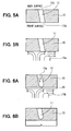
- a 4H-SiC single crystal substrate which has an off-surface inclined at 8 degrees from a (0 0 0 1) surface, and has a thickness of 300 ⁇ m (FIG. 5A).
- the substrate 10 is heated up to 1800 °C while hydrogen is flowed as a carrier gas 13a at a reduced pressure of, for example, 200 Torr (FIG. 5B).
- a back surface of the substrate 10 contacts the susceptor while the front surface of the substrate is subjected to hydrogen.
- flow rate of hydrogen is faster, such as 1 m/sec or more in the reduced pressure of 200 Torr. Therefore, heat is apt to be taken away from the front surface of the substrate 10, so that temperature at the front surface is kept low.
- a mix gas in which the SiH 4 gas and C 3 H 8 gas as source gases are added to the hydrogen gas is flowed, so that a SiC epitaxial film 14 is grown on the front surface of the substrate 10.
- a flow of the hydrogen gas is at 10 litters/min.
- the source gases flow with the hydrogen toward the substrate, so that the sublimation gas sublimed from the vicinity of the back surface of the substrate 10 cannot exit from the front surface to the outside of the substrate 10, so that recrystallization on an inner wall of the micro-pipe defect 11 at the vicinity of the front surface is encouraged.
- crystals increases which are recrystallized at the inner wall of the micro-pipe defect 11, at last, the micro-pipe defect 11 is occluded while the epitaxial film grows on that, so that the micro-pipe does not extend in the epitaxial film 14 (FIGS. 6A and 6B).
- a direction of the gas flow and a disposed orientation of the substrate are not limited to the case shown in FIG. 4.
- the gases may flow from an upper side and the front surface of the substrate may be oriented the upper side.
- a 6H-SiC single crystal substrate which has an off-surface inclined at 3.5 degrees from a (0 0 0 1) surface.
- the substrate is disposed in a susceptor 30, and inserted in the reactor of the CVD apparatus (FIG. 7A).
- the substrate 10 is heated up to 1800 °C while hydrogen is flowed as a carrier gas 13a at a reduced pressure of, for example, 200 Torr (FIG. 5B), and the substrate 10 is kept at that condition for 10 minutes.
- defect is selectively etched by exposing a front surface of the substrate to hydrogen at high temperature of approximately 1800 °C, so that an opening 12c of a micro-pipe 11 that is located at the front surface as shown in FIG. 7B is enlarged in comparison with a diameter of the micro-pipe (a bottom of the opening 12c).
- the micro-pipe has a pipe portion 12d and the opening portion 12c therein.
- a diameter of the opening 12c at a top thereof is twice or more as large as that at a bottom thereof where the pipe portion 12d is connected.
- SiH 4 gas and C 3 H 8 gas as source gases are introduced to form a SiC epitaxial film 14 on the front surface of the substrate.
- the epitaxial film 14 grows while a growth in a lateral direction is encouraged, which is faster than that on the front surface, by synergistic effect in which a plurality of steps is formed at an enlarged opening as cores for growth, and a surface of the opening approximates the a-surface from a face orientation of the front surface.
- a thickness of the epitaxial film becomes thicker, and finally the micro-pipe 11 is occluded, and the epitaxial film grows on that. Therefore, the micro-pipe defect 11 is not inherited into the epitaxial film (FIGS. 8A and 8B).
- the micro-pipe defect 11 is encouraged being occluded by a sublimation gas of SiC.
- a gas containing chlorine instead of hydrogen may be introduced to obtain the similar effect.
- chlorine it is unnecessary to heat up the substrate.
- hydrogen it is preferable that the substrate is heated up to 1650 °C or more. This is because etching effect by using hydrogen is not apt to appear at low temperature, and therefore it takes long time to enlarge the opening at the surface of the micro-pipe defect 11.
- the depletion layer When a depletion layer reaches the micro-pipe defect, a breakdown occurs. In this case, the breakdown voltage is lower than that expected. Therefore, it is preferable that the depletion layer does not reach the micro-pipe defect.
- FIG. 9A shows a n + -type low resistivity substrate 20 in which impurities are introduced at high concentration (for example, 10 19 to 10 20 /cm 3 ) and on which a high resistivity, n - -type epitaxial film 14 is formed by method described above.
- FIG. 9 shows the low resistivity substrate 20 on which the n - -type epitaxial film 14 having low impurity concentration.
- a p-type region is formed in or on the n - -type epitaxial film 14 to serve as a device, and when a reverse bias is applied to a p-n junction formed in the substrate, it may be supposed a case where the depletion layer expands to penetrate the n - -type epitaxial film 14 and reach the SiC substrate 20. Since an impurity concentration of the SiC substrate 20 is high, the depletion layer hardly expands in the SiC substrate 20.
- the depletion layer does not reach the micro-pipe defect 11, and therefore the breakdown due to the micro-pipe defect 11 is prevent from occurring.
- FIG. 9B shows the n + -type low resistivity substrate 20 on which a low resistivity n + -type epitaxial film 21 similar to the substrate 20 is formed, and a high resistivity, n - -type epitaxial film 22 is formed on the low resistivity n+-type epitaxial film 21.
- n + -type epitaxial film 21 is formed at 1750 °C or less. Also in this case, similarly to the case shown in FIG. 9A, it is preferable that the micro-pipe defect 11 is occluded in the low resistivity region since the micro-pipe defect 11 may not influence the withstand voltage.
- the micro-pipe defect should be occluded in a conductive low resistivity region.
- conductive means a low resistivity region to which impurities are introduced to such a degree that this region can serve as a conductor.
- FIG. 10 shows a modification of the structure, shown in FIG. 4, to hold the SiC substrate 10 in the CVD apparatus.
- a substrate holder 37 protrudes from a side face of the susceptor 30 to hold SiC substrate 10.
- a heat equalizer 38 composed of carbon is disposed on the back surface of the SiC substrate 10 so as to closely contact the back surface of the SiC substrate 10. All portions of the SiC substrate 10 are equally heated up to the temperature by the heat equalizer 38.
- the micro-pipe defect penetrates the SiC substrate 10
- the micro-pipe defect is occluded at the front surface of the SiC substrate 10
- the sublimation gas sublimed from the vicinity of the back surface of the SiC substrate 10 is apt to move to the front surface of the SiC substrate 10 in epitaxial growth.
- the occlusion of the micro-pipe defect is encouraged.
- the heat equalizer 38 does not contact the SiC substrate 10 with a space interposed therebetween, but contacts the substrate holder 37.
- the substrate holder 37 holds entire periphery of the SiC substrate 10 to form a closed space between the heat equalizer 38 and the SiC substrate 10. Therefore, a pressure due to the closed space is applied to the back surface of the SiC substrate 10 while a decompressive atmosphere exists on the front surface of the SiC substrate 10 at such a degree of, for example, 200 Torr which is low pressure as compared to the back surface.
- the heat equalizer 38 may not contact the substrate holder 37, and a narrowed space may be formed between the heat equalizer 38 and the SiC substrate 10 that is narrow at several mm or less.
- the sublimation gas sublimed from the vicinity of the back surface of the SiC substrate 10 is apt to move to the front surface of the SiC substrate 10, so that the occlusion of the micro-pipe defect is encouraged at the front surface of the SiC substrate 10.
- a pressure difference between the front surface and the back surface of the substrate 10 is generated, i.e., the pressure applied to the front surface is lowered in comparison with the back surface to encourage the occlusion of the micro-pipe defect.
- the substrate holder 37 has an opening at a portion other than the region to contact the SiC substrate 10 so that the gas flowing into the susceptor 30 from the lower side is exhausted from the upper side of the susceptor 30.
- the temperature of the SiC substrate is at 1650 °C or more since sublimation is apt to occur from the SiC substrate at this temperature condition.
- the temperature is at 1750 °C or more, preferably 1800 °C or more.
- the temperature of the SiC substrate exceeds 1900 °C, sublimation is encouraged rather than recrystallization, so that there is possibility that the micro-pipe defect cannot be occluded. Therefore, the temperature is preferably set at 1900 °C or less.
- the temperature can be at 1900 °C or more, for example, approximately at 2250 °C which is a temperature of a seed crystal substrate in the sublimation method when the conditions of the growth rate, the atmosphere in the growth and the like can be suitably set.
- the flow rate of the carrier gas or the gas for the epitaxial growth is preferably set at 1 m/sec or more.
- the temperature difference between the front surface and the back surface of the SiC substrate is set at 0.5 °C or more, preferably set at 5 °C or more.
- the sublimation gas from the vicinity of the back surface of the SiC substrate is transferred to the front surface and is apt to be recrystallized through the micro-pipe defect.
- the thickness of the SiC substrate is at 300 ⁇ m or more, the temperature difference between the front surface and the back surface is apt to be generated.
- the growth rate of the epitaxial film to be formed on the front surface of the SiC substrate at 20 ⁇ m/h or more, preferably 30 ⁇ m/h or more, the growth rate toward the lateral direction (a-face growth) approximately perpendicular to the thickness direction of the substrate can be enhanced, so that the micro-pipe defect can be prevented from being inherited into the epitaxial film.
- the present invention is not limited to provide a substrate for device, but may be employed in a bulk growth by utilizing a merit that the growth rate of the epitaxial film is fast.
- SiC single crystals can be obtained in which micro-pipe defects are eliminated.
- the SiC substrate, on which the epitaxial layer is grown by the method as described above to occlude the micro-pipe defect can be employed as a seed crystal for the so-called sublimation method in which SiC source powder or source gases are sublimed to be recrystallized on the seed crystal so as to form a bulk SiC.
- sublimed gases are recrystallized on the epitaxial film disposed in a chamber composed of, for example, carbon.
- the growth method is not limited to the CVD method, but can employ a vapor phase deposition method such as molecular epitaxial growth method, sublimation method or the like.
Landscapes
- Chemical & Material Sciences (AREA)
- Engineering & Computer Science (AREA)
- Crystallography & Structural Chemistry (AREA)
- Materials Engineering (AREA)
- Metallurgy (AREA)
- Organic Chemistry (AREA)
- Inorganic Chemistry (AREA)
- Chemical Kinetics & Catalysis (AREA)
- General Chemical & Material Sciences (AREA)
- Crystals, And After-Treatments Of Crystals (AREA)
Abstract
Description
Claims (27)
- A manufacturing method of silicon carbide single crystals, comprising the steps of:providing a silicon carbide single-crystal substrate (10, 20) having a micro-pipe (11) therein;applying temperature difference in a thickness direction of the substrate so that temperature at a front surface of the substrate is lower than that at a back surface of the substrate that is disposed opposite to the front surface;supplying a gas (34) containing at least carbon and a gas (34) containing at least silicon to the front surface to form a silicon carbide film (14, 21, 22) by epitaxial growth.
- A manufacturing method of silicon carbide single crystals according to claim 1, wherein temperature of the substrate is set at 1650 °C or more.
- A manufacturing method of silicon carbide single crystals according to claim 2, wherein the temperature of the substrate is set in a range from 1750 to 1900 °C.
- A manufacturing method of silicon carbide single crystals according to claim 1, wherein the temperature difference is caused by supplying a gas containing hydrogen or helium to the front surface of the substrate.
- A manufacturing method of silicon carbide single crystals according to any one of claims 2 to 4, wherein flow rate of the gas containing carbon and the gas containing silicon is set at 1 m/sec or more just before reaching the substrate.
- A manufacturing method of silicon carbide single crystals according to any one of claims 1 to 5, wherein the temperature difference is set at 0.5 °C or more.
- A manufacturing method of silicon carbide single crystals according claim 6, wherein the temperature difference is set at 5 °C or more.
- A manufacturing method of silicon carbide single crystals according to any one of claims 1 to 7, wherein the silicon carbide film includes a film formed by epitaxial growth in which a growth rate is at 20 µm/h or more.
- A manufacturing method of silicon carbide single crystals according to any one of claims 1 to 8, wherein a thickness of the substrate is 300 µm or more.
- A manufacturing method of silicon carbide single crystals forming a silicon carbide film (14, 21, 22) by epitaxial growth on a silicon carbide substrate (10, 20) having a micro-pipe (11), comprising the steps of:holding said substrate by a holding means (30); andsetting flow direction of a gas containing carbon and a gas containing silicon in approximately perpendicular to a front surface of the substrate that has an opening of said micro-pipe, so that said silicon carbide film is formed on the front surface of the silicon carbide substrate by epitaxial growth, wherein flow rate of the gas containing carbon and the gas containing silicon is set 1 m/sec or more.
- A manufacturing method of silicon carbide single crystals according to claim 10, wherein temperature of the surface of the substrate is set at 1650 °C or more.
- A manufacturing method of silicon carbide single crystals according to claim 11, wherein the temperature of the surface of the substrate is set in a range from 1750 to 1900 °C.
- A manufacturing method of silicon carbide single crystals according to any one of claims 10 to 12, wherein said micro-pipe penetrates the substrate from the front surface to a back surface thereof, and the substrate is held so that the back surface thereof closely contacts a contacting member.
- A manufacturing method of silicon carbide single crystals according to any one of claims 10 to 12, wherein said micro-pipe penetrates the substrate from the front surface to a back surface thereof, and the substrate is held so that pressure of an atmosphere contacting the back surface is high as compared to that of an atmosphere contacting the front surface.
- A manufacturing method of silicon carbide single crystals according to any one of claims 10 to 14, wherein the silicon carbide film is formed by the epitaxial growth in reduced pressure.
- A manufacturing method for forming silicon carbide single crystals (14, 21, 22) on a silicon carbide substrate (10, 20) having a micro-pipe (11), comprising the steps of:modifying step for enlarging an opening (12c) of the micro-pipe that is disposed at a front surface of the substrate; andfilm growing step for forming a silicon carbide film (14, 21, 22) by epitaxial growth supplying a gas (34) containing at least carbon and a gas (34) containing at least a silicon to the front surface of the substrate.
- A manufacturing method for forming silicon carbide single crystals according to claim 16, wherein the substrate is heated up to 1650 °C or more while a carrier gas containing hydrogen flows on the front surface of the silicon carbide substrate in the modifying step.
- A manufacturing method for forming silicon carbide single crystals according to claim 16, wherein a carrier gas containing chlorine flows on the front surface of the silicon carbide substrate in the modifying step.
- A manufacturing method for forming silicon carbide single crystals according to claim 16, wherein the silicon carbide substrate is etched using KOH in the modifying step.
- A manufacturing method for forming silicon carbide single crystals according to any one of claims 16 to 19, wherein. the opening of the micro-pipe is enlarged so that a diameter thereof becomes twice or more in size as compared to that before enlarged.
- A manufacturing method for forming silicon carbide single crystals according to any one of claims 1 to 20, further comprising:disposing the silicon carbide substrate (10, 20) on which the silicon carbide film (14, 21, 22) is formed by the epitaxial growth in a chamber as a seed crystal;supplying a sublimation gas sublimed from a source material in the chamber; andrecrystallizing the sublimation gas on the seed crystal.
- A silicon carbide substrate comprising:a silicon carbide single crystal body (10, 20) having a micro-pipe (11) which is hollow and has a pipe-shaped portion and an opening (12c) whose diameter increases as being close to a front surface of said substrate, the pipe portion being located at a side of a back surface of the silicon carbide single crystal body, and the opening being located at a side of the front surface of the silicon carbide single crystal body; anda silicon carbide epitaxial film (14, 21, 22) formed on the front surface of the silicon carbide single crystal body so as to cover the micro-pipe, wherein the micro-pipe is eliminated in the silicon carbide single crystal body.
- A silicon carbide substrate according to claim 22, wherein:the diameter of the opening, which is enlarged at a top thereof, is twice or more as large as that of the opening at a bottom thereof where the pipe portion is connected.
- A silicon carbide substrate comprising:a conductive silicon carbide substrate body (10, 20) having a micro-pipe (11); anda silicon carbide epitaxial film (14, 21, 22) formed on a front surface of the substrate, wherein:the silicon carbide epitaxial film covers the micro-pipe, and the micro-pipe is eliminated at a conductive region (10, 20, 21) which is located between the conductive silicon carbide substrate body and the silicon carbide epitaxial film.
- A silicon carbide substrate according to claim 24, wherein said conductive region is the conductive substrate body.
- A silicon carbide substrate according to claim 24, wherein said conductive region is the conductive epitaxial film.
- A silicon carbide substrate according to claim 24, wherein the conductive epitaxial film has a low resistive epitaxial film (21) and a high resistive epitaxial film (22) formed on the low resistive epitaxial film, wherein said conductive region is the low resistive epitaxial film.
Applications Claiming Priority (2)
| Application Number | Priority Date | Filing Date | Title |
|---|---|---|---|
| JP2000377485 | 2000-12-12 | ||
| JP2000377485A JP4716558B2 (en) | 2000-12-12 | 2000-12-12 | Silicon carbide substrate |
Publications (3)
| Publication Number | Publication Date |
|---|---|
| EP1215311A2 true EP1215311A2 (en) | 2002-06-19 |
| EP1215311A3 EP1215311A3 (en) | 2006-08-02 |
| EP1215311B1 EP1215311B1 (en) | 2010-02-10 |
Family
ID=18846200
Family Applications (1)
| Application Number | Title | Priority Date | Filing Date |
|---|---|---|---|
| EP01129641A Expired - Lifetime EP1215311B1 (en) | 2000-12-12 | 2001-12-12 | Manufacturing method of silicon carbide single crystals |
Country Status (4)
| Country | Link |
|---|---|
| US (2) | US6746787B2 (en) |
| EP (1) | EP1215311B1 (en) |
| JP (1) | JP4716558B2 (en) |
| DE (1) | DE60141268D1 (en) |
Families Citing this family (30)
| Publication number | Priority date | Publication date | Assignee | Title |
|---|---|---|---|---|
| JP4716558B2 (en) * | 2000-12-12 | 2011-07-06 | 株式会社デンソー | Silicon carbide substrate |
| DE10211312A1 (en) * | 2002-03-14 | 2003-10-02 | Wacker Siltronic Halbleitermat | Epitaxial coating applying method of semiconductor wafer in chemical vapor deposition reactor, involves exposing back surface of semiconductor wafer to ejection gas containing specific amount of hydrogen |
| US7175704B2 (en) * | 2002-06-27 | 2007-02-13 | Diamond Innovations, Inc. | Method for reducing defect concentrations in crystals |
| JP4150642B2 (en) * | 2003-08-04 | 2008-09-17 | 株式会社デンソー | Single crystal growth method and growth apparatus |
| US7018554B2 (en) * | 2003-09-22 | 2006-03-28 | Cree, Inc. | Method to reduce stacking fault nucleation sites and reduce forward voltage drift in bipolar devices |
| JP4874527B2 (en) | 2004-04-01 | 2012-02-15 | トヨタ自動車株式会社 | Silicon carbide semiconductor substrate and method for manufacturing the same |
| JP4976647B2 (en) * | 2004-07-29 | 2012-07-18 | 富士電機株式会社 | Method for manufacturing silicon carbide semiconductor substrate |
| JP5224256B2 (en) * | 2005-06-02 | 2013-07-03 | 学校法人関西学院 | Single crystal silicon carbide substrate processing method, semiconductor device manufacturing method |
| US20070169687A1 (en) * | 2006-01-26 | 2007-07-26 | Caracal, Inc. | Silicon carbide formation by alternating pulses |
| JP5087238B2 (en) * | 2006-06-22 | 2012-12-05 | 株式会社ニューフレアテクノロジー | Semiconductor manufacturing apparatus maintenance method and semiconductor manufacturing method |
| JP2008001569A (en) * | 2006-06-23 | 2008-01-10 | Shin Etsu Chem Co Ltd | Single crystal SiC, method for manufacturing the same, and apparatus for manufacturing single crystal SiC |
| JP2009544849A (en) * | 2006-07-27 | 2009-12-17 | レール・リキード−ソシエテ・アノニム・プール・レテュード・エ・レクスプロワタシオン・デ・プロセデ・ジョルジュ・クロード | Film forming apparatus cleaning method and film forming apparatus |
| WO2008014434A2 (en) * | 2006-07-28 | 2008-01-31 | Caracal, Inc. | Crystal growth method and reactor design |
| JP5045272B2 (en) * | 2007-07-03 | 2012-10-10 | 富士電機株式会社 | Method for manufacturing single crystal silicon carbide substrate |
| JP4827829B2 (en) * | 2007-12-18 | 2011-11-30 | 三菱電機株式会社 | Method for manufacturing silicon carbide semiconductor substrate and method for manufacturing silicon carbide semiconductor device |
| JP5360639B2 (en) * | 2008-02-05 | 2013-12-04 | 学校法人関西学院 | Surface modified single crystal SiC substrate, single crystal SiC substrate with epitaxial growth layer, semiconductor chip, seed substrate for single crystal SiC growth, and method for producing polycrystalline SiC substrate with single crystal growth layer |
| JP2009256159A (en) * | 2008-04-14 | 2009-11-05 | Incubation Alliance Inc | Manufacturing method of crystalline silicon carbide substrate |
| JP4978637B2 (en) * | 2009-02-12 | 2012-07-18 | 株式会社デンソー | Method for producing silicon carbide single crystal |
| CN102427971B (en) * | 2009-04-14 | 2015-01-07 | 速力斯公司 | High efficiency epitaxial chemical vapor deposition (cvd) reactor |
| JP5415853B2 (en) * | 2009-07-10 | 2014-02-12 | 東京エレクトロン株式会社 | Surface treatment method |
| JP2011077502A (en) * | 2009-09-04 | 2011-04-14 | Hitachi Kokusai Electric Inc | Thermal treatment apparatus |
| CA2753709A1 (en) * | 2010-01-26 | 2011-08-04 | Sumitomo Electric Industries, Ltd. | Method of manufacturing silicon carbide substrate |
| CA2759074A1 (en) * | 2010-02-05 | 2011-08-11 | Taro Nishiguchi | Method for manufacturing silicon carbide substrate |
| JP5481224B2 (en) * | 2010-02-19 | 2014-04-23 | 株式会社ニューフレアテクノロジー | Film forming apparatus and film forming method |
| US9870937B2 (en) | 2010-06-09 | 2018-01-16 | Ob Realty, Llc | High productivity deposition reactor comprising a gas flow chamber having a tapered gas flow space |
| JP5573725B2 (en) * | 2011-02-21 | 2014-08-20 | セイコーエプソン株式会社 | Method for manufacturing cubic silicon carbide semiconductor substrate |
| TW201427052A (en) * | 2012-11-05 | 2014-07-01 | Nusola Inc | Wide energy gap photovoltaic device and method of manufacturing same |
| CN110476223B (en) * | 2017-04-04 | 2023-05-30 | 三菱电机株式会社 | Method for manufacturing silicon carbide epitaxial wafer and method for manufacturing silicon carbide semiconductor device |
| CN110331437B (en) * | 2019-07-11 | 2020-04-24 | 浙江博蓝特半导体科技股份有限公司 | Silicon carbide single crystal growth apparatus and method for producing silicon carbide single crystal |
| CN111172586B (en) * | 2020-01-03 | 2025-07-25 | 北京北方华创微电子装备有限公司 | Epitaxial reaction chamber |
Family Cites Families (26)
| Publication number | Priority date | Publication date | Assignee | Title |
|---|---|---|---|---|
| US4912063A (en) * | 1987-10-26 | 1990-03-27 | North Carolina State University | Growth of beta-sic thin films and semiconductor devices fabricated thereon |
| JPH07131067A (en) * | 1993-11-08 | 1995-05-19 | Sanyo Electric Co Ltd | Method for manufacturing silicon carbide wafer and method for manufacturing silicon carbide light emitting diode element |
| US5679153A (en) | 1994-11-30 | 1997-10-21 | Cree Research, Inc. | Method for reducing micropipe formation in the epitaxial growth of silicon carbide and resulting silicon carbide structures |
| JPH0952796A (en) * | 1995-08-18 | 1997-02-25 | Fuji Electric Co Ltd | SiC crystal growth method and SiC semiconductor device |
| US5944890A (en) * | 1996-03-29 | 1999-08-31 | Denso Corporation | Method of producing single crystals and a seed crystal used in the method |
| JPH1036194A (en) * | 1996-07-23 | 1998-02-10 | Hitachi Ltd | Silicon carbide vapor phase crystal growth equipment |
| JPH10125905A (en) * | 1996-10-17 | 1998-05-15 | Denso Corp | Semiconductor substrate and method of straightening semiconductor substrate |
| JPH10261615A (en) * | 1997-03-17 | 1998-09-29 | Fuji Electric Co Ltd | Method for controlling surface morphology of SiC semiconductor and method for growing SiC semiconductor thin film |
| JP3296998B2 (en) | 1997-05-23 | 2002-07-02 | 日本ピラー工業株式会社 | Single crystal SiC and method for producing the same |
| US6153166A (en) | 1997-06-27 | 2000-11-28 | Nippon Pillar Packing Co., Ltd. | Single crystal SIC and a method of producing the same |
| JPH11162850A (en) * | 1997-08-27 | 1999-06-18 | Matsushita Electric Ind Co Ltd | Silicon carbide substrate, method of manufacturing the same, and semiconductor element using silicon carbide substrate |
| JP3043690B2 (en) * | 1997-11-17 | 2000-05-22 | 日本ピラー工業株式会社 | Single crystal SiC and method for producing the same |
| JP3508519B2 (en) * | 1997-11-28 | 2004-03-22 | 松下電器産業株式会社 | Epitaxial growth apparatus and epitaxial growth method |
| JP2884085B1 (en) * | 1998-04-13 | 1999-04-19 | 日本ピラー工業株式会社 | Single crystal SiC and method for producing the same |
| JP3414321B2 (en) * | 1998-05-29 | 2003-06-09 | 株式会社デンソー | Method for producing silicon carbide single crystal |
| DE69916177T2 (en) * | 1998-05-29 | 2005-04-14 | Denso Corp., Kariya | Method for producing a silicon carbide monocrystal |
| JPH11354789A (en) * | 1998-06-12 | 1999-12-24 | Nissan Motor Co Ltd | Field effect transistor |
| JP2000026199A (en) * | 1998-07-09 | 2000-01-25 | Denso Corp | Method for producing silicon carbide single crystal and silicon carbide single crystal |
| JP2917149B1 (en) | 1998-07-13 | 1999-07-12 | 日本ピラー工業株式会社 | Single crystal SiC and method for producing the same |
| JP2000044397A (en) * | 1998-07-31 | 2000-02-15 | Toyota Central Res & Dev Lab Inc | Method for producing silicon carbide single crystal |
| JP3248071B2 (en) * | 1998-10-08 | 2002-01-21 | 日本ピラー工業株式会社 | Single crystal SiC |
| JP3043744B1 (en) * | 1999-03-17 | 2000-05-22 | 日本ピラー工業株式会社 | Method for growing single crystal SiC |
| JP3443379B2 (en) * | 1999-03-23 | 2003-09-02 | 松下電器産業株式会社 | Method for growing semiconductor film and method for manufacturing semiconductor device |
| DE60020737T2 (en) * | 1999-09-06 | 2006-03-16 | Sixon Inc. | SIC-EINKRISTALL AND MANUFACTURING METHOD THEREFOR |
| JP4716558B2 (en) * | 2000-12-12 | 2011-07-06 | 株式会社デンソー | Silicon carbide substrate |
| US6780243B1 (en) * | 2001-11-01 | 2004-08-24 | Dow Corning Enterprises, Inc. | Method of silicon carbide monocrystalline boule growth |
-
2000
- 2000-12-12 JP JP2000377485A patent/JP4716558B2/en not_active Expired - Fee Related
-
2001
- 2001-12-10 US US10/006,135 patent/US6746787B2/en not_active Expired - Lifetime
- 2001-12-12 DE DE60141268T patent/DE60141268D1/en not_active Expired - Lifetime
- 2001-12-12 EP EP01129641A patent/EP1215311B1/en not_active Expired - Lifetime
-
2004
- 2004-04-27 US US10/832,396 patent/US7147714B2/en not_active Expired - Fee Related
Also Published As
| Publication number | Publication date |
|---|---|
| JP2002179498A (en) | 2002-06-26 |
| US7147714B2 (en) | 2006-12-12 |
| JP4716558B2 (en) | 2011-07-06 |
| US6746787B2 (en) | 2004-06-08 |
| DE60141268D1 (en) | 2010-03-25 |
| US20020069818A1 (en) | 2002-06-13 |
| EP1215311B1 (en) | 2010-02-10 |
| EP1215311A3 (en) | 2006-08-02 |
| US20040194693A1 (en) | 2004-10-07 |
Similar Documents
| Publication | Publication Date | Title |
|---|---|---|
| US7147714B2 (en) | Manufacturing method of silicon carbide single crystals | |
| EP1721031B1 (en) | Reduction of carrot defects in silicon carbide epitaxy | |
| JP3692076B2 (en) | SiC single crystal and growth method thereof | |
| CN102400224B (en) | Silicon carbide single crystal and manufacturing method of the same | |
| CN101027433B (en) | Seed and seed holder combination for high-quality growth of large SiC single crystals | |
| EP2264223A2 (en) | Micropipe-free silicon carbide and related method of manufacture | |
| EP1491662A1 (en) | METHOD FOR PREPARING SiC CRYSTAL AND SiC CRYSTAL | |
| EP0835336A1 (en) | A device and a method for epitaxially growing objects by cvd | |
| JP2006261612A (en) | Silicon carbide semiconductor and method and apparatus for manufacturing the same | |
| JP4253974B2 (en) | SiC single crystal and growth method thereof | |
| JP2002530266A (en) | Method of growing crystal on substrate | |
| Janzen et al. | SiC material for high-power applications | |
| EP1122341A1 (en) | Single crystal SiC | |
| EP3072995B1 (en) | Method for producing silicon carbide crystals from vapour phase | |
| JP2004262709A (en) | Method for growing SiC single crystal | |
| Lebedeva et al. | Growth and investigation of the big area Lely-grown substrates | |
| JP2917149B1 (en) | Single crystal SiC and method for producing the same | |
| JP2739469B2 (en) | Method for growing SiC film | |
| JPS6152119B2 (en) | ||
| Skowronski et al. | Silicon carbide epitaxy | |
| Schöner | New development in hot wall vapor phase epitaxial growth of silicon carbide | |
| Tsuchida et al. | Growth of thick and low‐doped 4H‐SiC epitaxial layers in a vertical radiant‐heating VPE reactor |
Legal Events
| Date | Code | Title | Description |
|---|---|---|---|
| PUAI | Public reference made under article 153(3) epc to a published international application that has entered the european phase |
Free format text: ORIGINAL CODE: 0009012 |
|
| AK | Designated contracting states |
Kind code of ref document: A2 Designated state(s): AT BE CH CY DE DK ES FI FR GB GR IE IT LI LU MC NL PT SE TR |
|
| AX | Request for extension of the european patent |
Free format text: AL;LT;LV;MK;RO;SI |
|
| PUAL | Search report despatched |
Free format text: ORIGINAL CODE: 0009013 |
|
| AK | Designated contracting states |
Kind code of ref document: A3 Designated state(s): AT BE CH CY DE DK ES FI FR GB GR IE IT LI LU MC NL PT SE TR |
|
| AX | Request for extension of the european patent |
Extension state: AL LT LV MK RO SI |
|
| 17P | Request for examination filed |
Effective date: 20061018 |
|
| 17Q | First examination report despatched |
Effective date: 20070309 |
|
| AKX | Designation fees paid |
Designated state(s): DE FI SE |
|
| GRAP | Despatch of communication of intention to grant a patent |
Free format text: ORIGINAL CODE: EPIDOSNIGR1 |
|
| GRAS | Grant fee paid |
Free format text: ORIGINAL CODE: EPIDOSNIGR3 |
|
| GRAA | (expected) grant |
Free format text: ORIGINAL CODE: 0009210 |
|
| AK | Designated contracting states |
Kind code of ref document: B1 Designated state(s): DE FI SE |
|
| REF | Corresponds to: |
Ref document number: 60141268 Country of ref document: DE Date of ref document: 20100325 Kind code of ref document: P |
|
| REG | Reference to a national code |
Ref country code: SE Ref legal event code: TRGR |
|
| PLBE | No opposition filed within time limit |
Free format text: ORIGINAL CODE: 0009261 |
|
| STAA | Information on the status of an ep patent application or granted ep patent |
Free format text: STATUS: NO OPPOSITION FILED WITHIN TIME LIMIT |
|
| 26N | No opposition filed |
Effective date: 20101111 |
|
| PGFP | Annual fee paid to national office [announced via postgrant information from national office to epo] |
Ref country code: FI Payment date: 20141211 Year of fee payment: 14 |
|
| PGFP | Annual fee paid to national office [announced via postgrant information from national office to epo] |
Ref country code: DE Payment date: 20161213 Year of fee payment: 16 |
|
| PGFP | Annual fee paid to national office [announced via postgrant information from national office to epo] |
Ref country code: SE Payment date: 20161221 Year of fee payment: 16 |
|
| PG25 | Lapsed in a contracting state [announced via postgrant information from national office to epo] |
Ref country code: FI Free format text: LAPSE BECAUSE OF NON-PAYMENT OF DUE FEES Effective date: 20151212 |
|
| REG | Reference to a national code |
Ref country code: DE Ref legal event code: R119 Ref document number: 60141268 Country of ref document: DE |
|
| PG25 | Lapsed in a contracting state [announced via postgrant information from national office to epo] |
Ref country code: SE Free format text: LAPSE BECAUSE OF NON-PAYMENT OF DUE FEES Effective date: 20171213 |
|
| PG25 | Lapsed in a contracting state [announced via postgrant information from national office to epo] |
Ref country code: DE Free format text: LAPSE BECAUSE OF NON-PAYMENT OF DUE FEES Effective date: 20180703 |