EP1214778B1 - Arrangement for the protection of a power semiconductor output stage switching an inductive consumer - Google Patents
Arrangement for the protection of a power semiconductor output stage switching an inductive consumer Download PDFInfo
- Publication number
- EP1214778B1 EP1214778B1 EP00960316A EP00960316A EP1214778B1 EP 1214778 B1 EP1214778 B1 EP 1214778B1 EP 00960316 A EP00960316 A EP 00960316A EP 00960316 A EP00960316 A EP 00960316A EP 1214778 B1 EP1214778 B1 EP 1214778B1
- Authority
- EP
- European Patent Office
- Prior art keywords
- power semiconductor
- excitation winding
- semiconductor output
- arrangement
- energy
- Prior art date
- Legal status (The legal status is an assumption and is not a legal conclusion. Google has not performed a legal analysis and makes no representation as to the accuracy of the status listed.)
- Expired - Lifetime
Links
Images
Classifications
-
- H—ELECTRICITY
- H02—GENERATION; CONVERSION OR DISTRIBUTION OF ELECTRIC POWER
- H02P—CONTROL OR REGULATION OF ELECTRIC MOTORS, ELECTRIC GENERATORS OR DYNAMO-ELECTRIC CONVERTERS; CONTROLLING TRANSFORMERS, REACTORS OR CHOKE COILS
- H02P25/00—Arrangements or methods for the control of AC motors characterised by the kind of AC motor or by structural details
- H02P25/02—Arrangements or methods for the control of AC motors characterised by the kind of AC motor or by structural details characterised by the kind of motor
- H02P25/08—Reluctance motors
- H02P25/092—Converters specially adapted for controlling reluctance motors
- H02P25/0925—Converters specially adapted for controlling reluctance motors wherein the converter comprises only one switch per phase
-
- Y—GENERAL TAGGING OF NEW TECHNOLOGICAL DEVELOPMENTS; GENERAL TAGGING OF CROSS-SECTIONAL TECHNOLOGIES SPANNING OVER SEVERAL SECTIONS OF THE IPC; TECHNICAL SUBJECTS COVERED BY FORMER USPC CROSS-REFERENCE ART COLLECTIONS [XRACs] AND DIGESTS
- Y10—TECHNICAL SUBJECTS COVERED BY FORMER USPC
- Y10S—TECHNICAL SUBJECTS COVERED BY FORMER USPC CROSS-REFERENCE ART COLLECTIONS [XRACs] AND DIGESTS
- Y10S388/00—Electricity: motor control systems
- Y10S388/90—Specific system operational feature
- Y10S388/903—Protective, e.g. voltage or current limit
Definitions
- the invention relates to an arrangement for the protection of MOS FETs in low-side circuit formed power semiconductor power amplifiers, depending on a control signal opposing energizing windings of an electronically commutated Motors or oppositely wound coils of a switching relay or a contactor with a common magnetic circuit to a DC supply voltage turn on and off of this, using energy transformatory from a field winding or coil on the as an additional inductance acting other excitation winding or coil is transferable with a Resistor loaded or in counter-current direction with the DC supply voltage is coupled, and wherein the additional inductance for an energized Excitation winding in each case those in the commutation cycle below oppositely energized excitation winding is.
- Such an arrangement for protecting a power semiconductor output stage is in DE 296 22 254 U1.
- two phase windings connected via switches alternately to a voltage source.
- magnetic field energy stored in its inductance i. during the Energization of electrical energy not converted into kinetic energy, is transformed to the other phase winding by means of transformer coupling transferred to its inductance.
- This will be a big part of not in Kinetic energy convertible residual energy recuperatively from one to the other Phase winding and shifted back again.
- MOS-FETs or bipolar transistors In connection with the use of IGBT's, MOS-FETs or bipolar transistors is running that the overvoltage that occurs when the energized inductance is switched off additional diodes in a so used for both switches RC-relief network is transferred.
- the cut-off energy is when switching off the series connection to the additional inductance, i.e. a separate circuit from the series, transmitted and dissipated in this by stress. It can by appropriate Coupling of the additional inductance the released energy also to the DC supply voltage be transferred back. With the specified Measures can be dispensed with freewheeling diodes. With the N-channel Mos-FETs Low-side switching results in particularly simple circuits.
- the design is easier Way made so that the inductive load and the additional inductance as oppositely wound coils formed with common magnetic circuit are.
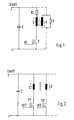
- FIG. 1 used for switching on and off of the inductive Consumer L an N-channel MOS FET designated T.
- the control takes place with a control signal st, which when queuing the power semiconductor output stage T fully energized, so that the power loss of the same is as small as possible and the maximum current through the consumer L with the Consumer resistance RL can flow. It falls on the consumer L practical the full DC supply voltage Ubatt. Will the power semiconductor power amplifier T no longer activated by switching off the control signal st, then it assumes the high-impedance switching state, in which for the induction voltage of the load L, the parasitic diode of the power semiconductor power amplifier forms a circuit.
- the induction voltage becomes transferred to an additional inductance Lz, which transforms with the consumer L is coupled, i. the consumer L and the additional inductance Lz are opposing windings with common magnetic circuit. Is the additional inductance Lz loaded with a resistor R, then the energy of the Induction degraded. However, the energy can also - like the dashed lines of Fig. 1 show - in the opposite direction to the DC supply voltage Ubatt with the parallel-connected smoothing capacitor C back become.
- the circuit diagram of Fig. 2 shows as inductive loads L1 and L2, the two Exciter windings of an electronically commutatable motor.
- the consumers L1 and L2 are alternately energized, wherein from step to step the Bestromungscardi the excitation windings changes, since they are included in the series circuits with opposite winding sense are.
- the power semiconductor output stages T1 and T2 are in the commutation cycle with the successive control signals st1, st2, st1, st2 ... charged.
- the transformer acts coupled consumers L2 as additional inductance Lz, while in the Energizing the load L2 of the load L1 the function of the additional inductance Lz takes over.
- the circuit works in every energizing phase 2 as the circuit of FIG. 1, so that also here no freewheeling diodes consumers I1 and L2, i. the excitation windings of the engine required are and the power semiconductor power amplifiers T1 and T2 compared to the shutdown occurring induction voltages are protected.
Landscapes
- Engineering & Computer Science (AREA)
- Power Engineering (AREA)
- Inverter Devices (AREA)
- Control Of Ac Motors In General (AREA)
- Control Of Motors That Do Not Use Commutators (AREA)
- Control Of Direct Current Motors (AREA)
Description
Die Erfindung betrifft eine Anordnung zum Schutz von mit MOS-FETs in Low-Side-Schaltung gebildeten Leistungshalbleiter-Endstufen, die in Abhängigkeit eines Steuersignals gegensinnige Erregerwicklungen eines elektronisch kommutierbaren Motors oder gegensinnig gewickelte Spulen eines Schaltrelais oder eines Schaltschützes mit gemeinsamem Magnetkreis an eine Gleichstrom-Versorgungsspannung anschalten und von dieser abschalten, wobei Energie transformatorisch von einer Erregerwicklung oder Spule auf die als Zusatzinduktivität wirkende andere Erregerwicklung oder Spule übertragbar ist, die mit einem Widerstand belastet oder in Gegenstromrichtung mit der Gleichstrom-Versorgungsspannung gekoppelt ist, und wobei die Zusatzinduktivität für eine bestromte Erregerwicklung jeweils die im Kommutierungszyklus nachfolgend gegensinnig bestromte Erregerwicklung ist.The invention relates to an arrangement for the protection of MOS FETs in low-side circuit formed power semiconductor power amplifiers, depending on a control signal opposing energizing windings of an electronically commutated Motors or oppositely wound coils of a switching relay or a contactor with a common magnetic circuit to a DC supply voltage turn on and off of this, using energy transformatory from a field winding or coil on the as an additional inductance acting other excitation winding or coil is transferable with a Resistor loaded or in counter-current direction with the DC supply voltage is coupled, and wherein the additional inductance for an energized Excitation winding in each case those in the commutation cycle below oppositely energized excitation winding is.
Eine derartige Anordnung zum Schutz einer Leistungshalbleiter-Endstufe ist in der DE 296 22 254 U1 angegeben. Bei dieser bekannten Anordnung werden zwei Phasenwicklungen über Schalter alternierend an eine Spannungsquelle angeschlossen. Die während der Bestromung einer der beiden Phasenwicklungen in deren Induktivität gespeicherte magnetische Feldenergie, d.h. die während der Bestromung nicht in Bewegungsenergie umgesetzte elektrische Restenergie, wird mittels transformatorischer Kopplung auf die jeweils andere Phasenwicklung in dessen Induktivität transferiert. Dadurch wird ein großer Teil der nicht in Bewegungsenergie umsetzbaren Restenergie rekuperativ von einer in die andere Phasenwicklung und wieder zurück geshiftet. Im Zusammenhang mit der Verwendung von IGBT's, MOS-FETs oder Bipolartransistoren ist ausgeführt, dass die beim Abschalten der bestromten Induktivität auftretende Überspannung über zusätzliche Dioden in ein für beide Schalter gleichsam verwendetes RC-Entlastungsnetzwerk transferiert wird.Such an arrangement for protecting a power semiconductor output stage is in DE 296 22 254 U1. In this known arrangement two phase windings connected via switches alternately to a voltage source. During energization of one of the two phase windings magnetic field energy stored in its inductance, i. during the Energization of electrical energy not converted into kinetic energy, is transformed to the other phase winding by means of transformer coupling transferred to its inductance. This will be a big part of not in Kinetic energy convertible residual energy recuperatively from one to the other Phase winding and shifted back again. In connection with the use of IGBT's, MOS-FETs or bipolar transistors is running that the overvoltage that occurs when the energized inductance is switched off additional diodes in a so used for both switches RC-relief network is transferred.
Bei in der US-A 4,164,696 und der WO 93/23918 A angegebenen weiteren Anordnungen zum Ansteuern von Phasenwicklungen elektrischer Motoren werden Phasenwicklungen ebenfalls über Steuereinrichtungen mit Leistungshalbleitern angesteuert, wobei aufeinanderfolgende Wicklungen transformatorisch gekoppelt sind. In further arrangements specified in US Pat. No. 4,164,696 and WO 93/23918 A. for driving phase windings of electric motors Phase windings also via control devices with power semiconductors controlled, with successive windings transformer coupled are.
Weitere derartige Reihenschaltungen aus Leistungshalbleiter-Endstufe und induktivem Verbraucher werden für verschiedene Anwendungen eingesetzt. Dabei wird mit dem Steuersignal die Leistungshalbleiter-Endstufe stets voll durchgesteuert, um ihre Verlustleistung möglichst klein zu halten. Beim Abschalten der Leistungshalbleiter-Endstufe entsteht am induktiven Verbraucher eine Abschaltenergie W = ½ LI2, die von der Leistungshalbleiter-Endstufe ferngehalten werden muss, da diese über die parasitäre Diode derselben einen Stromfluss erzeugen würde, der zu einer Überlastung oder Zerstörung der Leistungshalbleiter-Endstufe führen könnte. Um dies zu verhindern, wird dem Verbraucher eine sogenannte Freilaufdiode parallel geschaltet, die als Leistungsdiode an die geschaltete Leistung der Reihenschaltung anzupassen ist und daher sehr teuer ist.Further such series circuits of power semiconductor output stage and inductive load are used for various applications. In this case, the power semiconductor output stage is always fully controlled by the control signal in order to keep their power loss as small as possible. When switching off the power semiconductor output stage, a cut-off energy W = ½ LI 2 arises at the inductive load, which must be kept away from the power semiconductor output stage, since this would generate a current flow via the parasitic diode thereof, which would overload or destroy the power semiconductor output stage could lead. To prevent this, the consumer is connected in parallel with a so-called freewheeling diode, which is to be adapted as a power diode to the switched power of the series circuit and is therefore very expensive.
Wie die WO 96/09683 zeigt, ist es bei elektronisch kommutierbaren Motoren auch bekannt, in den Freilaufkreis einer Erregerwicklung jeweils die nachfolgend zu bestromende Erregerwicklung einzubeziehen und so bereits eine Vormagnetisierung zu erreichen. Diese Anordnung benötigt jedoch nach wie vor die Freilaufdiode als Koppeldioden zwischen den Erregerwicklungen.As WO 96/09683 shows, it is in electronically commutatable motors Also known in the freewheeling circuit of a field winding in each case the following To include energizing excitation winding and so already a bias to reach. However, this arrangement still requires the freewheeling diode as coupling diodes between the exciter windings.
Es ist Aufgabe der Erfindung, eine Anordnung der eingangs erwähnten Art zu schaffen, die bei vereinfachtem Aufbau die Abschaltenergie des induktiven Verbrauchers von der Leistungshalbleiter-Endstufe fernhält und abführt.It is an object of the invention to provide an arrangement of the type mentioned create, with a simplified structure, the cut-off of the inductive Consumer away from the power semiconductor power amplifier and dissipates.
Diese Aufgabe wird bei einer Anordnung der eingangs erwähnten Art nach der Erfindung dadurch gelöst, dass die beim Abschalten am induktiven Verbraucher auftretende Abschaltenergie auf die Zusatzinduktivität übertragbar ist und dass die Leistungshalbleiter-Endstufen N-Kanal-MOS-FETs sind, wobei eine parasitäre Diode des jeweiligen MOS-FET beim Abschalten des Steuersignals einen Stromkreis mit verringertem Stromfluss bildet. This object is achieved in an arrangement of the type mentioned according to the invention in that the shutdown At the inductive load occurring cut-off energy to the additional inductance is transferable and that the power semiconductor power amplifiers N-channel MOS FETs are, wherein a parasitic diode of the respective MOS-FET at shutdown of the control signal forms a circuit with reduced current flow.
Die Abschaltenergie wird beim Abschalten der Reihenschaltung auf die Zusatzinduktivität, d.h. einen von der Reihenschaltung getrennten Kreis, übertragen und in diesem durch Belastung abgeführt. Dabei kann durch entsprechende Kopplung der Zusatzinduktivität die frei werdende Energie auch zur Gleichstrom-Versorgungsspannung zurück übertragen werden. Mit den angegebenen Maßnahmen kann auf Freilaufdioden verzichtet werden. Mit den N-Kanal-Mos-FETs in Low-Side-Schaltung ergeben sich besonders einfache Schaltungen.The cut-off energy is when switching off the series connection to the additional inductance, i.e. a separate circuit from the series, transmitted and dissipated in this by stress. It can by appropriate Coupling of the additional inductance the released energy also to the DC supply voltage be transferred back. With the specified Measures can be dispensed with freewheeling diodes. With the N-channel Mos-FETs Low-side switching results in particularly simple circuits.
Bei einem Schaltrelais und einem Schaltschütz ist die Auslegung in einfacher Weise so getroffen, dass der induktive Verbraucher und die Zusatzinduktivität als gegensinnig gewickelte Spulen mit gemeinsamem Magnetkreis ausgebildet sind.For a switching relay and a contactor, the design is easier Way made so that the inductive load and the additional inductance as oppositely wound coils formed with common magnetic circuit are.
Für einen elektronisch steuerbaren Motor ist die Zusatzinduktivität für eine bestromte Erregerwicklung jeweils die im Kommutierungszyklus nachfolgend gegensinnig bestromte Erregerwicklung.For an electronically controllable motor is the additional inductance for a energized exciter winding in each case following in the commutation cycle oppositely energized excitation winding.
Die Erfindung wird anhand von in der Zeichnung dargestellten Ausführungsbeispielen näher erläutert. Es zeigen:
- Fig. 1
- eine Anordnung mit einem über eine Leistungshalbleiter-Endstufe geschalteten Schaltrelais und
- Fig. 2
- eine Anordnung mit einem elektronisch kommutierbaren Motor mit vier Polen und zwei Wickelsträngen als Erregerwicklungen.
- Fig. 1
- an arrangement with a switched via a power semiconductor output stage switching relay and
- Fig. 2
- an arrangement with an electronically commutatable motor with four poles and two winding strands as exciter windings.
Das Ausführungsbeispiel nach Fig. 1 verwendet zum An- und Abschalten des induktiven Verbrauchers L einen mit T bezeichneten N-Kanal-MOS-FET. Die Ansteuerung erfolgt mit einem Steuersignal st, das beim Anstehen die Leistungshalbleiter-Endstufe T voll durchsteuert, so dass die Verlustleistung derselben möglichst klein ist und der maximale Strom durch den Verbraucher L mit dem Verbraucherwiderstand RL fließen kann. Dabei fällt am Verbraucher L praktisch die volle Gleichstrom-Versorgungsspannung Ubatt ab. Wird die Leistungshalbleiter-Endstufe T durch Abschalten des Steuersignals st nicht mehr angesteuert, dann nimmt sie den hochohmigen Schaltzustand ein, in dem für die Induktionsspannung des Verbrauchers L die parasitäre Diode der Leistungshalbleiter-Endstufe einen Stromkreis bildet.The embodiment of FIG. 1 used for switching on and off of the inductive Consumer L an N-channel MOS FET designated T. The control takes place with a control signal st, which when queuing the power semiconductor output stage T fully energized, so that the power loss of the same is as small as possible and the maximum current through the consumer L with the Consumer resistance RL can flow. It falls on the consumer L practical the full DC supply voltage Ubatt. Will the power semiconductor power amplifier T no longer activated by switching off the control signal st, then it assumes the high-impedance switching state, in which for the induction voltage of the load L, the parasitic diode of the power semiconductor power amplifier forms a circuit.
Um einen Stromfluss darüber stark zu verringern, wird die Induktionsspannung auf eine Zusatzinduktivität Lz übertragen, die transformatorisch mit dem Verbraucher L gekoppelt ist, d.h. der Verbraucher L und die Zusatzinduktivität Lz sind gegensinnige Wicklungen mit gemeinsamem Magnetkreis. Ist die Zusatzinduktivität Lz mit einem Widerstand R belastet, dann wird damit die Energie der Induktion abgebaut. Die Energie kann jedoch auch - wie die gestrichelten Linien der Fig. 1 zeigen - in Gegenstromrichtung auf die Gleichstrom-Versorgungsspannung Ubatt mit dem parallel geschalteten Glättungskondensator C zurück übertragen werden.To greatly reduce current flow therethrough, the induction voltage becomes transferred to an additional inductance Lz, which transforms with the consumer L is coupled, i. the consumer L and the additional inductance Lz are opposing windings with common magnetic circuit. Is the additional inductance Lz loaded with a resistor R, then the energy of the Induction degraded. However, the energy can also - like the dashed lines of Fig. 1 show - in the opposite direction to the DC supply voltage Ubatt with the parallel-connected smoothing capacitor C back become.
Das Schaltbild nach Fig. 2 zeigt als induktive Verbraucher L1 und L2 die zwei Erregerwicklungen eines elektronisch kommutierbaren Motors. In dem Kommutierungszyklus werden die Verbraucher L1 und L2 abwechselnd bestromt, wobei sich von Schritt zu Schritt die Bestromungsrichtung der Erregerwicklungen ändert, da sie in die Reihenschaltungen mit gegensinnigem Wicklungssinn einbezogen sind. Die Leistungshalbleiter-Endstufen T1 und T2 werden im Kommutierungszyklus mit den aufeinander folgenden Steuersignalen st1, st2, st1, st2 ... beaufschlagt. Bei der Bestromung des Verbrauchers L1 wirkt der transformatorisch gekoppelte Verbraucher L2 als Zusatzinduktivität Lz, während bei der Bestromung des Verbrauchers L2 der Verbraucher L1 die Funktion der Zusatzinduktivität Lz übernimmt. In jeder Bestromungsphase arbeitet die Schaltung nach Fig.2 wie die Schaltung nach Fig. 1, so das auch hier keine Freilaufdioden an den Verbrauchern I1 und L2, d.h. den Erregerwicklungen des Motors erforderlich sind und die Leistungshalbleiter-Endstufen T1 und T2 gegenüber der beim Abschalten auftretenden Induktionsspannungen geschützt sind.The circuit diagram of Fig. 2 shows as inductive loads L1 and L2, the two Exciter windings of an electronically commutatable motor. In the commutation cycle the consumers L1 and L2 are alternately energized, wherein from step to step the Bestromungsrichtung the excitation windings changes, since they are included in the series circuits with opposite winding sense are. The power semiconductor output stages T1 and T2 are in the commutation cycle with the successive control signals st1, st2, st1, st2 ... charged. When energizing the load L1, the transformer acts coupled consumers L2 as additional inductance Lz, while in the Energizing the load L2 of the load L1 the function of the additional inductance Lz takes over. The circuit works in every energizing phase 2 as the circuit of FIG. 1, so that also here no freewheeling diodes consumers I1 and L2, i. the excitation windings of the engine required are and the power semiconductor power amplifiers T1 and T2 compared to the shutdown occurring induction voltages are protected.
Claims (1)
- Arrangement for protecting power semiconductor output stages (Tl, T2) which are formed with MOSFETs in a low-side circuit and, in a manner dependent on a control signal, connect opposing excitation windings (L1, L2) of an electronically commutatable motor or coils (which have been wound in the opposite sense) of a switching relay or of a switching contactor having a common magnetic circuit to a DC supply voltage and disconnect them from the latter, it being possible for energy to be transmitted, by means of a transformer, from one excitation winding (L1) or coil to the other excitation winding (L2) or coil that acts as an additional inductor (Lz) and is loaded by means of a resistor (R) or is coupled, in the counter-current direction, to the DC supply voltage (Ubatt), and, in the case of an electronically commutated motor, the additional inductor for an energized excitation winding (e.g. L1) respectively being the excitation winding (L2) that is subsequently energized in the opposite sense in the commutation cycle,
characterized in that
the turn-off energy W = ½ LI2 that arises at the inductive load (L, L1, L2) during turn-off can be transmitted to the additional inductor (Lz, L2, L1), and
in that the power semiconductor output stages (T, Tl, T2) are N-channel MOSFETs, a parasitic diode of the respective MOSFET forming a circuit with reduced current flow when the control signal (st) is turned off.
Applications Claiming Priority (3)
| Application Number | Priority Date | Filing Date | Title |
|---|---|---|---|
| DE19941698 | 1999-09-02 | ||
| DE19941698A DE19941698A1 (en) | 1999-09-02 | 1999-09-02 | Arrangement for protecting a power semiconductor output stage switching an inductive consumer |
| PCT/DE2000/002421 WO2001018950A1 (en) | 1999-09-02 | 2000-07-25 | Arrangement for the protection of a power semiconductor output stage switching an inductive consumer |
Publications (2)
| Publication Number | Publication Date |
|---|---|
| EP1214778A1 EP1214778A1 (en) | 2002-06-19 |
| EP1214778B1 true EP1214778B1 (en) | 2005-05-04 |
Family
ID=7920466
Family Applications (1)
| Application Number | Title | Priority Date | Filing Date |
|---|---|---|---|
| EP00960316A Expired - Lifetime EP1214778B1 (en) | 1999-09-02 | 2000-07-25 | Arrangement for the protection of a power semiconductor output stage switching an inductive consumer |
Country Status (6)
| Country | Link |
|---|---|
| US (1) | US6888327B1 (en) |
| EP (1) | EP1214778B1 (en) |
| JP (1) | JP4612259B2 (en) |
| DE (2) | DE19941698A1 (en) |
| ES (1) | ES2241650T3 (en) |
| WO (1) | WO2001018950A1 (en) |
Family Cites Families (18)
| Publication number | Priority date | Publication date | Assignee | Title |
|---|---|---|---|---|
| US3684934A (en) * | 1971-01-11 | 1972-08-15 | Superior Electric Co | Stepping motor drive circuit with path for induced voltages |
| US4164696A (en) * | 1977-08-10 | 1979-08-14 | Teletype Corporation | Stepping motor excitation |
| DE2829685C2 (en) * | 1978-07-06 | 1982-09-09 | Danfoss A/S, 6430 Nordborg | Motor fed by DC voltage |
| US4275339A (en) * | 1979-12-21 | 1981-06-23 | International Business Machines Corporation | Bifilar brushless DC motor |
| DE3010435A1 (en) * | 1980-03-19 | 1981-09-24 | Papst-Motoren Kg, 7742 St Georgen | COLLECTORLESS DC MOTOR |
| US4347464A (en) * | 1981-03-02 | 1982-08-31 | General Electric Company | FET Motor drive system |
| JPS61244292A (en) * | 1985-04-20 | 1986-10-30 | Osaka Denki Kk | Speed controller for dc motor |
| AT386096B (en) * | 1985-11-28 | 1988-06-27 | Schrack Elektronik Ag | FLOW CONVERTER WITH A DC INPUT CIRCUIT |
| JPS62147842A (en) | 1985-12-21 | 1987-07-01 | Ricoh Co Ltd | Communication control equipment |
| US5376851A (en) * | 1992-05-18 | 1994-12-27 | Electric Power Research Institute, Inc. | Variable reluctance motor with full and short pitch windings |
| US5291115A (en) * | 1992-09-25 | 1994-03-01 | The Texas A&M University System | Method and apparatus for sensing the rotor position of a switched reluctance motor without a shaft position sensor |
| CA2151532C (en) * | 1994-07-25 | 1998-12-22 | Emerson Electric Co. | Auxiliary starting switched reluctance motor |
| US6262510B1 (en) | 1994-09-22 | 2001-07-17 | Iancu Lungu | Electronically switched reluctance motor |
| JP3069507B2 (en) * | 1995-03-28 | 2000-07-24 | 松下電工株式会社 | DC motor controller |
| US5729112A (en) * | 1996-07-26 | 1998-03-17 | Dana Corporation | Phase current sensing in a bifilar-wound switched reluctance motor drive topology |
| DE29622254U1 (en) * | 1996-12-21 | 1998-04-16 | Aeg Hausgeraete Gmbh | Power electronics for a synchronous motor |
| DE19934668A1 (en) * | 1999-07-23 | 2001-01-25 | Bosch Gmbh Robert | Electronically commutated motor |
| JP2001128480A (en) * | 1999-10-26 | 2001-05-11 | Moriyama Manufacturing Co Ltd | Permanent magnet two-phase dc brushless motor |
-
1999
- 1999-09-02 DE DE19941698A patent/DE19941698A1/en not_active Ceased
-
2000
- 2000-07-25 JP JP2001522655A patent/JP4612259B2/en not_active Expired - Lifetime
- 2000-07-25 US US10/070,879 patent/US6888327B1/en not_active Expired - Lifetime
- 2000-07-25 EP EP00960316A patent/EP1214778B1/en not_active Expired - Lifetime
- 2000-07-25 WO PCT/DE2000/002421 patent/WO2001018950A1/en active IP Right Grant
- 2000-07-25 ES ES00960316T patent/ES2241650T3/en not_active Expired - Lifetime
- 2000-07-25 DE DE50010245T patent/DE50010245D1/en not_active Expired - Lifetime
Also Published As
| Publication number | Publication date |
|---|---|
| DE19941698A1 (en) | 2001-03-15 |
| JP2003509996A (en) | 2003-03-11 |
| JP4612259B2 (en) | 2011-01-12 |
| WO2001018950A1 (en) | 2001-03-15 |
| EP1214778A1 (en) | 2002-06-19 |
| ES2241650T3 (en) | 2005-11-01 |
| US6888327B1 (en) | 2005-05-03 |
| DE50010245D1 (en) | 2005-06-09 |
Similar Documents
| Publication | Publication Date | Title |
|---|---|---|
| DE69625119T2 (en) | Power plant | |
| EP1145416B1 (en) | Inverter for conversion of electrical energy | |
| WO2006089605A1 (en) | Method for operation of a two-phase electronically-commuted motor and motor for carrying out said method | |
| DE102007029388A1 (en) | Self-supplied switch circuit for use in pulse width modulated current source rectifier, has snubber circuit and self-powered supply circuit forming series circuit between circuit nodes in parallel with switching device | |
| DE19835316A1 (en) | Controlled rectifier bridge with surge protection | |
| EP1459434B1 (en) | Circuit arrangement for operating an electrical machine | |
| DE19838296A1 (en) | Dual voltage power supply for an on-board vehicle mains supply, includes a current generator that is coupled to the a battery and a rectifier/convertor arrangement | |
| DE69727553T2 (en) | HIGH PERFORMANCE ELECTRIC MOTOR WITH ELECTRONIC COMMUTATION | |
| EP0682402A1 (en) | Output magnitudes rise limiting device for self-commutated constant voltage intermediate circuit converter | |
| US6204729B1 (en) | H-bridge power amplifier for a motor | |
| DE69838358T2 (en) | Electronically commutated motor | |
| EP1214778B1 (en) | Arrangement for the protection of a power semiconductor output stage switching an inductive consumer | |
| DE2739387A1 (en) | Vehicle electric current supply controller - has single magnetic circuit regulating two separate inductor systems | |
| EP0947043A1 (en) | Power electronic unit for a synchronous motor | |
| EP2238674A2 (en) | Load control circuit in a motor vehicle control device | |
| EP2985898A1 (en) | DC/DC converter having two modes of operation | |
| EP0806827B1 (en) | Reverse battery protection circuit | |
| DE3049020C2 (en) | Controllable DC / DC converter for power switch-mode power supplies | |
| EP1226647B1 (en) | Method for controlling at least one inductive consumer by means of a pulse width modulated control signal | |
| DE69826405T2 (en) | Single-phase asynchronous motor with two windings | |
| DE3005156C2 (en) | Rectifier arrangement in three-phase bridge circuit | |
| EP3192173A1 (en) | Half bridge having two semiconductor switches for operating a load | |
| DE202020001077U1 (en) | Circuit arrangement for speed control of a synchronous motor | |
| DE3932762A1 (en) | Electronically-commutated DC machine - has auxiliary electronic power switch supplied with modulated clock pulses to control speed | |
| DE2410926A1 (en) | Supply and braking circuit for DC motor - has thyristors in rectifier shorting back-EMF and braking rotor when motor supply fails |
Legal Events
| Date | Code | Title | Description |
|---|---|---|---|
| PUAI | Public reference made under article 153(3) epc to a published international application that has entered the european phase |
Free format text: ORIGINAL CODE: 0009012 |
|
| 17P | Request for examination filed |
Effective date: 20020402 |
|
| AK | Designated contracting states |
Kind code of ref document: A1 Designated state(s): AT BE CH CY DE DK ES FI FR GB GR IE IT LI LU MC NL PT SE |
|
| 17Q | First examination report despatched |
Effective date: 20030915 |
|
| RBV | Designated contracting states (corrected) |
Designated state(s): DE ES FR GB IT |
|
| GRAP | Despatch of communication of intention to grant a patent |
Free format text: ORIGINAL CODE: EPIDOSNIGR1 |
|
| GRAS | Grant fee paid |
Free format text: ORIGINAL CODE: EPIDOSNIGR3 |
|
| GRAA | (expected) grant |
Free format text: ORIGINAL CODE: 0009210 |
|
| AK | Designated contracting states |
Kind code of ref document: B1 Designated state(s): DE ES FR GB IT |
|
| PG25 | Lapsed in a contracting state [announced via postgrant information from national office to epo] |
Ref country code: GB Free format text: LAPSE BECAUSE OF FAILURE TO SUBMIT A TRANSLATION OF THE DESCRIPTION OR TO PAY THE FEE WITHIN THE PRESCRIBED TIME-LIMIT Effective date: 20050504 |
|
| REG | Reference to a national code |
Ref country code: GB Ref legal event code: FG4D Free format text: NOT ENGLISH |
|
| REG | Reference to a national code |
Ref country code: IE Ref legal event code: FG4D Free format text: LANGUAGE OF EP DOCUMENT: GERMAN |
|
| REF | Corresponds to: |
Ref document number: 50010245 Country of ref document: DE Date of ref document: 20050609 Kind code of ref document: P |
|
| REG | Reference to a national code |
Ref country code: ES Ref legal event code: FG2A Ref document number: 2241650 Country of ref document: ES Kind code of ref document: T3 |
|
| GBV | Gb: ep patent (uk) treated as always having been void in accordance with gb section 77(7)/1977 [no translation filed] |
Effective date: 20050504 |
|
| PLBE | No opposition filed within time limit |
Free format text: ORIGINAL CODE: 0009261 |
|
| STAA | Information on the status of an ep patent application or granted ep patent |
Free format text: STATUS: NO OPPOSITION FILED WITHIN TIME LIMIT |
|
| ET | Fr: translation filed | ||
| 26N | No opposition filed |
Effective date: 20060207 |
|
| REG | Reference to a national code |
Ref country code: FR Ref legal event code: PLFP Year of fee payment: 17 |
|
| REG | Reference to a national code |
Ref country code: DE Ref legal event code: R084 Ref document number: 50010245 Country of ref document: DE |
|
| REG | Reference to a national code |
Ref country code: FR Ref legal event code: PLFP Year of fee payment: 18 |
|
| REG | Reference to a national code |
Ref country code: FR Ref legal event code: PLFP Year of fee payment: 19 |
|
| PGFP | Annual fee paid to national office [announced via postgrant information from national office to epo] |
Ref country code: FR Payment date: 20190724 Year of fee payment: 20 Ref country code: IT Payment date: 20190723 Year of fee payment: 20 Ref country code: DE Payment date: 20190924 Year of fee payment: 20 Ref country code: ES Payment date: 20190822 Year of fee payment: 20 |
|
| REG | Reference to a national code |
Ref country code: DE Ref legal event code: R071 Ref document number: 50010245 Country of ref document: DE |
|
| REG | Reference to a national code |
Ref country code: ES Ref legal event code: FD2A Effective date: 20201106 |
|
| PG25 | Lapsed in a contracting state [announced via postgrant information from national office to epo] |
Ref country code: ES Free format text: LAPSE BECAUSE OF EXPIRATION OF PROTECTION Effective date: 20200726 |