EP1214744B1 - Silicon strain gage having a thin layer of highly conductive silicon - Google Patents
Silicon strain gage having a thin layer of highly conductive silicon Download PDFInfo
- Publication number
- EP1214744B1 EP1214744B1 EP00950526A EP00950526A EP1214744B1 EP 1214744 B1 EP1214744 B1 EP 1214744B1 EP 00950526 A EP00950526 A EP 00950526A EP 00950526 A EP00950526 A EP 00950526A EP 1214744 B1 EP1214744 B1 EP 1214744B1
- Authority
- EP
- European Patent Office
- Prior art keywords
- layer
- silicon
- wafer
- thickness
- electrically conductive
- Prior art date
- Legal status (The legal status is an assumption and is not a legal conclusion. Google has not performed a legal analysis and makes no representation as to the accuracy of the status listed.)
- Expired - Lifetime
Links
- 229910052710 silicon Inorganic materials 0.000 title claims description 54
- 239000010703 silicon Substances 0.000 title claims description 54
- XUIMIQQOPSSXEZ-UHFFFAOYSA-N Silicon Chemical compound [Si] XUIMIQQOPSSXEZ-UHFFFAOYSA-N 0.000 title claims description 48
- 239000000758 substrate Substances 0.000 claims description 22
- 238000000034 method Methods 0.000 claims description 14
- 239000004065 semiconductor Substances 0.000 claims description 13
- 238000005530 etching Methods 0.000 claims description 8
- 239000000463 material Substances 0.000 claims description 7
- 238000000059 patterning Methods 0.000 claims description 7
- 230000008021 deposition Effects 0.000 claims description 5
- 229910021421 monocrystalline silicon Inorganic materials 0.000 claims description 5
- 239000012159 carrier gas Substances 0.000 claims description 4
- 239000013078 crystal Substances 0.000 claims description 4
- 239000002019 doping agent Substances 0.000 claims description 3
- 230000001105 regulatory effect Effects 0.000 claims description 3
- 239000011248 coating agent Substances 0.000 claims description 2
- 238000000576 coating method Methods 0.000 claims description 2
- 230000001276 controlling effect Effects 0.000 claims description 2
- 235000012431 wafers Nutrition 0.000 description 16
- 238000000151 deposition Methods 0.000 description 5
- 230000000694 effects Effects 0.000 description 3
- 230000008901 benefit Effects 0.000 description 2
- 238000009792 diffusion process Methods 0.000 description 2
- 239000011521 glass Substances 0.000 description 2
- 238000005468 ion implantation Methods 0.000 description 2
- 238000004519 manufacturing process Methods 0.000 description 2
- 238000005259 measurement Methods 0.000 description 2
- VXEGSRKPIUDPQT-UHFFFAOYSA-N 4-[4-(4-methoxyphenyl)piperazin-1-yl]aniline Chemical compound C1=CC(OC)=CC=C1N1CCN(C=2C=CC(N)=CC=2)CC1 VXEGSRKPIUDPQT-UHFFFAOYSA-N 0.000 description 1
- UFHFLCQGNIYNRP-UHFFFAOYSA-N Hydrogen Chemical compound [H][H] UFHFLCQGNIYNRP-UHFFFAOYSA-N 0.000 description 1
- PNEYBMLMFCGWSK-UHFFFAOYSA-N aluminium oxide Inorganic materials [O-2].[O-2].[O-2].[Al+3].[Al+3] PNEYBMLMFCGWSK-UHFFFAOYSA-N 0.000 description 1
- 238000007796 conventional method Methods 0.000 description 1
- 229910021419 crystalline silicon Inorganic materials 0.000 description 1
- 238000010438 heat treatment Methods 0.000 description 1
- 239000001257 hydrogen Substances 0.000 description 1
- 229910052739 hydrogen Inorganic materials 0.000 description 1
- 239000011810 insulating material Substances 0.000 description 1
- 239000002184 metal Substances 0.000 description 1
- 238000000206 photolithography Methods 0.000 description 1
- 230000000704 physical effect Effects 0.000 description 1
- 230000035945 sensitivity Effects 0.000 description 1
- 150000003377 silicon compounds Chemical class 0.000 description 1
- 239000005049 silicon tetrachloride Substances 0.000 description 1
- 238000001947 vapour-phase growth Methods 0.000 description 1
Images
Classifications
-
- G—PHYSICS
- G01—MEASURING; TESTING
- G01L—MEASURING FORCE, STRESS, TORQUE, WORK, MECHANICAL POWER, MECHANICAL EFFICIENCY, OR FLUID PRESSURE
- G01L1/00—Measuring force or stress, in general
- G01L1/18—Measuring force or stress, in general using properties of piezo-resistive materials, i.e. materials of which the ohmic resistance varies according to changes in magnitude or direction of force applied to the material
-
- G—PHYSICS
- G01—MEASURING; TESTING
- G01L—MEASURING FORCE, STRESS, TORQUE, WORK, MECHANICAL POWER, MECHANICAL EFFICIENCY, OR FLUID PRESSURE
- G01L1/00—Measuring force or stress, in general
- G01L1/20—Measuring force or stress, in general by measuring variations in ohmic resistance of solid materials or of electrically-conductive fluids; by making use of electrokinetic cells, i.e. liquid-containing cells wherein an electrical potential is produced or varied upon the application of stress
- G01L1/22—Measuring force or stress, in general by measuring variations in ohmic resistance of solid materials or of electrically-conductive fluids; by making use of electrokinetic cells, i.e. liquid-containing cells wherein an electrical potential is produced or varied upon the application of stress using resistance strain gauges
- G01L1/2287—Measuring force or stress, in general by measuring variations in ohmic resistance of solid materials or of electrically-conductive fluids; by making use of electrokinetic cells, i.e. liquid-containing cells wherein an electrical potential is produced or varied upon the application of stress using resistance strain gauges constructional details of the strain gauges
- G01L1/2293—Measuring force or stress, in general by measuring variations in ohmic resistance of solid materials or of electrically-conductive fluids; by making use of electrokinetic cells, i.e. liquid-containing cells wherein an electrical potential is produced or varied upon the application of stress using resistance strain gauges constructional details of the strain gauges of the semi-conductor type
Definitions
- This invention relates to a silicon semiconductor strain gage, and in particular, to a silicon semiconductor strain gage comprising a thin layer of highly conductive silicon on a semi-insulating host substrate layer.
- Silicon is commonly used as a semiconductor sensor material because it exhibits many large physical effects to various applied sensitivities or signals and permits cost-efficient batch fabrication of sensors.
- One very useful effect that silicon exhibits is piezoresistance. This effect is exhibited by silicon in response to an applied a mechanical strain. This effect is considerable in silicon because the average mobility of electrons and holes therein is largely affected by strain.
- strain gages based on silicon semiconductor materials have been designed and are presently available. Many of these strain gages are fabricated from bulk single crystal silicon using conventional photolithography and etching techniques.
- a major disadvantage of such semiconductor strain gages is that their strain gage resistance depends directly on their thickness.
- the strain gage resistance from gage to gage can vary by a factor of 3 or more because current etching processes are incapable of maintaining thickness uniformity, on the order of 12 microns (0.0005 inches). This is mainly due to the pre-etching thickness of the gages which is typically about 152 microns (0.006 inches) and requires over 90% of the silicon to be removed. Overshooting the gage thickness by a mere 25 microns (0.001 inches) results in a 20% change in the gage's strain gage resistance.
- US 4,459,159 describes a method of making semi-insulating silicon substrate for semiconductor elements by post-process heating of oxygenated and doped silicon.
- a semiconductor strain gage comprising an electrically resistive substrate layer and a layer of electrically conductive silicon supported by the substrate layer.
- the silicon layer can be an epitaxial silicon layer grown on a surface of the substrate layer or a diffused or ion-implanted layer formed in the surface of the substrate layer.
- a force measuring and detecting device comprising a force responsive member and the above-described semiconductor strain gage attached to the force responsive member, the strain gage measuring forces applied to the force responsive member.
- a method of forming a plurality of semiconductor strain gages having substantially uniform resistance and being generally independent of the thickness of an electrically resistive silicon substrate layer comprising:
- the step of providing the crystalline or polycrystalline semi-insulating substate layer comprises providing a single crystal silicon substrate layer.
- the step of forming the epitaxial layer of electrically conductive silicon comprises forming a single crystal epitaxial layer of electrically conductive silicon.
- the step of forming the layer of electrically conductive silicon is accomplished by ion-implantation or diffusion.
- the method of the present invention further comprises patterning each strain gage into a serpentine shape.
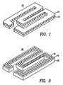
- FIG. 1 shows a perspective view of a silicon semiconductor strain gage 10 according to the present invention.
- the strain gage 10 of the invention is a piezoresistive device that utilizes a force to cause a resistance change due to mechanical strain.
- the strain gage 10 comprises a thin layer 14 of highly electrical-conductive (highly conductive) silicon of a desired conductivity type supported by a relatively highly electrical-resistive (highly resistive) host substrate layer 12.
- the host substrate layer 12 is typically composed of crystalline or polycrystalline semi-insulating material, such as intrinsic silicon or lightly doped (p or n type) silicon.
- the strain gage 10 of the invention is especially useful for measuring forces applied to metallic force responsive members of various configurations, such as beams, diaphragms, plates, rods and the like.
- force responsive members are commonly used in pressure measuring applications as strain gage pressure transducers, in weight measuring applications as strain gage load cells and strain gage transducers, and in other measuring and like applications which use force responsive members.
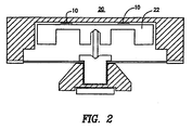
- FIG. 2 shows a typical force measuring and detecting device 20 that employs strain gages 10 of the invention.
- a typical force measuring and detecting device 20 that employs strain gages 10 of the invention.
- the device includes a metal force responsive member 22 with strain gages 10 according to the invention attached thereto using conventional glass bonding or other suitable attaching techniques.
- the strain gages are attached to the force responsive member in a Wheatstone bridge circuit.
- this device includes a force responsive member with four strain gages, one of ordinary skill in the art will recognize that force responsive members of other devices can employ as few as a single strain gage.
- the strain gage of the invention can be conventionally configured in an M or serpentine shape.
- many other available configurations have been previously described that are adapted for the direction and sense of the stresses or strains produced in a corresponding force responsive member in response to a force and/or are adapted for resistance changes produced by such stresses in crystalline silicon for a given conductivity type, crystal orientation and direction of current flow.
- the strain gage of the invention can be fabricated in virtually any of such strain gage configurations if desired.
- the highly conductive silicon layer comprises a 2-4 micron (0.00008-0.00017 inches) thick, 0.025-0.060 ohm-cm epitaxial silicon layer (epi-silicon layer), and the host substrate layer comprises an 8-10 micron (0.00033-0.00042 inches) thick, 10 ohm-cm or greater single crystal silicon layer.
- This strain gage embodiment can be made in bulk by growing an epi-silicon layer on an appropriately polished and cleaned surface of a single crystal silicon wafer using any conventional epitaxial deposition technique.
- Epitaxial deposition generally utilizes vapor-phase deposition in an epitaxial reactor.
- the polished and cleaned surface of the wafer is heated and the epi-silicon layer is deposited thereon by reacting hydrogen with a silicon compound such as silicon tetrachloride in a carrier gas.
- the thickness and the conductivity of the epi-layer of silicon can be controlled by regulating the deposition rates and introducing controlled amounts of suitable dopants into the carrier-gas stream.
- the epi-layer side of the wafer is patterned into individual strain gages using conventional photolithographic and etching techniques.
- the patterning typically ends about 12-14 microns into the wafer from the epi-layer side thereof.
- the substrate layer side of the wafer is then lapped from a starting thickness of about 380 microns (0.015 inches) to a thickness of about 100 microns.
- the epi-layer side of the wafer is coated with resist material and the wafer is chemically back-etched using conventional techniques until the pattern of the gages are visible to provide an overall gage thickness (including the epi-silicon layer) of 10 to 14 microns.
- the resist material is then conventionally removed and metallized electrical contacts are formed on the epi-silicon layer portion of the gages.
- FIG. 3 shows a strain gage 30 according to a second embodiment of the invention.
- a thin, highly conductive layer 36 is formed in a surface 34 of a silicon-based host substrate layer 32.
- This highly conductive layer can be formed by diffusion or ion-implantation.
- strain gage can also comprise a highly conductive epitaxial silicon layer grown on an insulating host substrate layer made from single crystal alumina or any other highly resistive material that permits epitaxial growth of silicon.
- the strain gage of the invention advantageously provides a strain gage resistance, which is generally independent of the overall thickness of the gage.
- a strain gage of the invention made from an 0.025 ohm-cm, 6 micron (0.00025 inches) thick epi-silicon layer grown on a host substrate of 25 ohm-cm silicon has the following resistance as a function of overall gage thickness: Overall gage Thickness Resistance 16.8 microns (0.0007 inches) 2994 ohms 14.4 microns (0.0006 inches) 2995 ohms 12.0 microns (0.0005 inches) 2997 ohms 9.6 microns (0.0004 inches) 2998 ohms 7.2 microns (0.0003 inches) 2999 ohms
- strain gage of the invention can be manufactured in large numbers with higher resistance values that are more uniform from gage to gage than conventional strain gages as demonstrated in Tables 1 and 2 below.
- Table 1 shows the resistance values of strain gages selected from 5 different wafers of strain gages of the invention and Table 2 shows the resistance values of strain gages selected from 5 different wafers of conventional strain gages. All the strain gages were of the same dimensions. The resistance measurements were obtained by glass bonding each selected strain gage to a 1830 micron (0.072 inch) thick beam-like force responsive member and applying the same force to each member.
- the strain gages of the invention boasted a mean resistance of about 4070 ohms, a maximum resistance of about 4460 ohms and a minimum resistance of about 3780 ohms.
- the standard and average standard deviations for these strain gages were 168.2 ohms and 97.1 ohms respectively and the percent average standard deviation was 2.39.
- the conventional strain gages of Table 2 demonstrated a mean resistance of only about 1399.8 ohms, a maximum resistance measuring about 1660 ohms and minimum resistance measuring about 1190 ohms.
- the standard deviation for these strain gages was 111.754 ohms and the standard deviation was 7.984.
Landscapes
- Physics & Mathematics (AREA)
- General Physics & Mathematics (AREA)
- Pressure Sensors (AREA)
Description
- This invention relates to a silicon semiconductor strain gage, and in particular, to a silicon semiconductor strain gage comprising a thin layer of highly conductive silicon on a semi-insulating host substrate layer.
- Silicon is commonly used as a semiconductor sensor material because it exhibits many large physical effects to various applied sensitivities or signals and permits cost-efficient batch fabrication of sensors. One very useful effect that silicon exhibits is piezoresistance. This effect is exhibited by silicon in response to an applied a mechanical strain. This effect is considerable in silicon because the average mobility of electrons and holes therein is largely affected by strain.
- Numerous strain gages based on silicon semiconductor materials have been designed and are presently available. Many of these strain gages are fabricated from bulk single crystal silicon using conventional photolithography and etching techniques.
- A major disadvantage of such semiconductor strain gages is that their strain gage resistance depends directly on their thickness. When manufactured in bulk, the strain gage resistance from gage to gage can vary by a factor of 3 or more because current etching processes are incapable of maintaining thickness uniformity, on the order of 12 microns (0.0005 inches). This is mainly due to the pre-etching thickness of the gages which is typically about 152 microns (0.006 inches) and requires over 90% of the silicon to be removed. Overshooting the gage thickness by a mere 25 microns (0.001 inches) results in a 20% change in the gage's strain gage resistance.
US 4,459,159 describes a method of making semi-insulating silicon substrate for semiconductor elements by post-process heating of oxygenated and doped silicon. - Accordingly, a need exists for a silicon strain gage with improved uniformity of strain gage resistance.
- In accordance with the invention, there is described a semiconductor strain gage comprising an electrically resistive substrate layer and a layer of electrically conductive silicon supported by the substrate layer. The silicon layer can be an epitaxial silicon layer grown on a surface of the substrate layer or a diffused or ion-implanted layer formed in the surface of the substrate layer.
- In further accordance with the invention, there is described a force measuring and detecting device comprising a force responsive member and the above-described semiconductor strain gage attached to the force responsive member, the strain gage measuring forces applied to the force responsive member.
- According to one aspect of the present invention there is provided a method of forming a plurality of semiconductor strain gages having substantially uniform resistance and being generally independent of the thickness of an electrically resistive silicon substrate layer, comprising:
- providing a wafer formed of a crystalline or polycrystalline semi-insulating, electrically resistive silicon substrate layer, said wafer having a front surface, a back surface, and a starting thickness of about 380 microns;
- forming an electrically conductive silicon layer on the front surface of the wafer of electrically resistive layer said layer being a grown epitaxial layer or an ion-implanted layer or a diffused layer;
- controlling the thickness and conductivity of the electrically conductive silicon layer by at least one of: regulating the deposition rate; and introducing controlled amount of dopants into a carrier gas stream;
- patterning the electrically conductive silicon layer into individual strain gages using an etching process, said patterning extending about 12-14 microns into the wafer;
- lapping the back surface of the wafer to a thickness of about 100 microns;
- coating the wafer with a resist material; and
- back etching the wafer until the pattern of strain gages are visible to provide an overall gage thickness in the range of 10-14 microns, whereby the resistance of the strain gage is substantially the resistance of the epitaxial layer of electrically conductive silicon and is independent of the thickness of the electrically resistive substrate layer.
- In one embodiment, the step of providing the crystalline or polycrystalline semi-insulating substate layer comprises providing a single crystal silicon substrate layer.
- In another embodiment, the step of forming the epitaxial layer of electrically conductive silicon comprises forming a single crystal epitaxial layer of electrically conductive silicon.
- In another embodiment, the step of forming the layer of electrically conductive silicon is accomplished by ion-implantation or diffusion.
- In another embodiment, the method of the present invention further comprises patterning each strain gage into a serpentine shape.
- The advantages, nature and various additional features of the invention will appear more fully upon consideration of the illustrative embodiments now to be described in detail in connection with accompanying drawings wherein:
- FIG. 1 is a perspective view of a silicon semiconductor strain gage according to an embodiment of the present invention;
- FIG. 2 is an elevational view of a force measuring and detecting device which employs the strain gage of the invention; and
- FIG. 3 is a perspective view of a silicon semiconductor strain gage according to a second embodiment of the invention.
- It should be understood that these drawings are for purposes of illustrating the concepts of the invention and are not to scale.
- FIG. 1 shows a perspective view of a silicon
semiconductor strain gage 10 according to the present invention. Thestrain gage 10 of the invention is a piezoresistive device that utilizes a force to cause a resistance change due to mechanical strain. Thestrain gage 10 comprises athin layer 14 of highly electrical-conductive (highly conductive) silicon of a desired conductivity type supported by a relatively highly electrical-resistive (highly resistive)host substrate layer 12. Thehost substrate layer 12 is typically composed of crystalline or polycrystalline semi-insulating material, such as intrinsic silicon or lightly doped (p or n type) silicon. - The
strain gage 10 of the invention is especially useful for measuring forces applied to metallic force responsive members of various configurations, such as beams, diaphragms, plates, rods and the like. Such force responsive members are commonly used in pressure measuring applications as strain gage pressure transducers, in weight measuring applications as strain gage load cells and strain gage transducers, and in other measuring and like applications which use force responsive members. - FIG. 2 shows a typical force measuring and detecting
device 20 that employsstrain gages 10 of the invention. Such a device is described in co-pendingU.S. Patent application no. 09/146,890 assigned to Measurement Specialties, Inc., the assignee herein. This Patent application shows an exemplary force measuring and detecting device which can utilize the strain gage device of the invention. The device includes a metal forceresponsive member 22 withstrain gages 10 according to the invention attached thereto using conventional glass bonding or other suitable attaching techniques. The strain gages are attached to the force responsive member in a Wheatstone bridge circuit. Although this device includes a force responsive member with four strain gages, one of ordinary skill in the art will recognize that force responsive members of other devices can employ as few as a single strain gage. - As can be seen by referring again to FIG. 1, the strain gage of the invention can be conventionally configured in an M or serpentine shape. However, many other available configurations have been previously described that are adapted for the direction and sense of the stresses or strains produced in a corresponding force responsive member in response to a force and/or are adapted for resistance changes produced by such stresses in crystalline silicon for a given conductivity type, crystal orientation and direction of current flow. It is contemplated that the strain gage of the invention can be fabricated in virtually any of such strain gage configurations if desired.
- In a typical embodiment of the strain gage of the invention (FIG. 1), the highly conductive silicon layer comprises a 2-4 micron (0.00008-0.00017 inches) thick, 0.025-0.060 ohm-cm epitaxial silicon layer (epi-silicon layer), and the host substrate layer comprises an 8-10 micron (0.00033-0.00042 inches) thick, 10 ohm-cm or greater single crystal silicon layer. This strain gage embodiment can be made in bulk by growing an epi-silicon layer on an appropriately polished and cleaned surface of a single crystal silicon wafer using any conventional epitaxial deposition technique.
- Epitaxial deposition generally utilizes vapor-phase deposition in an epitaxial reactor. In a typical process, the polished and cleaned surface of the wafer is heated and the epi-silicon layer is deposited thereon by reacting hydrogen with a silicon compound such as silicon tetrachloride in a carrier gas. The thickness and the conductivity of the epi-layer of silicon can be controlled by regulating the deposition rates and introducing controlled amounts of suitable dopants into the carrier-gas stream.
- After epitaxial deposition, the epi-layer side of the wafer is patterned into individual strain gages using conventional photolithographic and etching techniques. The patterning typically ends about 12-14 microns into the wafer from the epi-layer side thereof. The substrate layer side of the wafer is then lapped from a starting thickness of about 380 microns (0.015 inches) to a thickness of about 100 microns. After lapping, the epi-layer side of the wafer is coated with resist material and the wafer is chemically back-etched using conventional techniques until the pattern of the gages are visible to provide an overall gage thickness (including the epi-silicon layer) of 10 to 14 microns. The resist material is then conventionally removed and metallized electrical contacts are formed on the epi-silicon layer portion of the gages.
- FIG. 3 shows a
strain gage 30 according to a second embodiment of the invention. In this embodiment, a thin, highlyconductive layer 36 is formed in asurface 34 of a silicon-basedhost substrate layer 32. This highly conductive layer can be formed by diffusion or ion-implantation. - Although not shown, other embodiments of the strain gage can also comprise a highly conductive epitaxial silicon layer grown on an insulating host substrate layer made from single crystal alumina or any other highly resistive material that permits epitaxial growth of silicon.
- The strain gage of the invention advantageously provides a strain gage resistance, which is generally independent of the overall thickness of the gage. A strain gage of the invention made from an 0.025 ohm-cm, 6 micron (0.00025 inches) thick epi-silicon layer grown on a host substrate of 25 ohm-cm silicon has the following resistance as a function of overall gage thickness:
Overall gage Thickness Resistance 16.8 microns (0.0007 inches) 2994 ohms 14.4 microns (0.0006 inches) 2995 ohms 12.0 microns (0.0005 inches) 2997 ohms 9.6 microns (0.0004 inches) 2998 ohms 7.2 microns (0.0003 inches) 2999 ohms - Another benefit of the strain gage of the invention is that it can be manufactured in large numbers with higher resistance values that are more uniform from gage to gage than conventional strain gages as demonstrated in Tables 1 and 2 below. In particular, Table 1 shows the resistance values of strain gages selected from 5 different wafers of strain gages of the invention and Table 2 shows the resistance values of strain gages selected from 5 different wafers of conventional strain gages. All the strain gages were of the same dimensions. The resistance measurements were obtained by glass bonding each selected strain gage to a 1830 micron (0.072 inch) thick beam-like force responsive member and applying the same force to each member.


- Using data from Table 1, the strain gages of the invention boasted a mean resistance of about 4070 ohms, a maximum resistance of about 4460 ohms and a minimum resistance of about 3780 ohms. The standard and average standard deviations for these strain gages were 168.2 ohms and 97.1 ohms respectively and the percent average standard deviation was 2.39.
- In contrast, the conventional strain gages of Table 2 demonstrated a mean resistance of only about 1399.8 ohms, a maximum resistance measuring about 1660 ohms and minimum resistance measuring about 1190 ohms. The standard deviation for these strain gages was 111.754 ohms and the standard deviation was 7.984.
Claims (4)
- A method of forming a plurality of semiconductor strain gages having substantially uniform resistance and being generally independent of the thickness of an electrically resistive silicon substrate layer, comprising:providing a wafer formed of a crystalline or polycrystalline semi-insulating, electrically resistive silicon substrate layer, said wafer having a front surface, a back surface, and a starting thickness of about 380 microns;forming an electrically conductive silicon layer on the front surface of the wafer of electrically resistive silicon, said layer being a grown epitaxial layer or an ion-implanted layer or a diffused layer;controlling the thickness and conductivity of the electrically conductive silicon layer by at least one of: regulating the deposition rate; and introducing controlled amount of dopants into a carrier gas stream;patterning the electrically conductive silicon layer into individual strain gages using an etching process, said patterning extending about 12-14 microns into the wafer;lapping the back surface of the wafer to a thickness of about 100 microns;coating the wafer with a resist material; andback etching the wafer until the pattern of strain gages are visible to provide an overall gage thickness in the range of 10-14 microns, whereby the resistance of the strain gage is substantially the resistance of the epitaxial layer of electrically conductive silicon and is independent of the thickness of the electrically resistive substrate layer.
- The method according to claim 1, wherein the step of providing the crystalline or polycrystalline semi-insulating substrate layer comprises providing a single crystal silicon substrate layer.
- The method according to claim 1, wherein the step of forming the epitaxial layer of electrically conductive silicon comprises forming a single crystal epitaxial layer of electrically conductive silicon.
- The method of claim 1, further comprising patterning each strain gage into a serpentine shape.
Applications Claiming Priority (3)
| Application Number | Priority Date | Filing Date | Title |
|---|---|---|---|
| US09/359,012 US6635910B1 (en) | 1999-07-22 | 1999-07-22 | Silicon strain gage having a thin layer of highly conductive silicon |
| US359012 | 1999-07-22 | ||
| PCT/US2000/019911 WO2001008227A1 (en) | 1999-07-22 | 2000-07-21 | Silicon strain gage having a thin layer of highly conductive silicon |
Publications (3)
| Publication Number | Publication Date |
|---|---|
| EP1214744A1 EP1214744A1 (en) | 2002-06-19 |
| EP1214744A4 EP1214744A4 (en) | 2003-03-19 |
| EP1214744B1 true EP1214744B1 (en) | 2007-11-14 |
Family
ID=23411962
Family Applications (1)
| Application Number | Title | Priority Date | Filing Date |
|---|---|---|---|
| EP00950526A Expired - Lifetime EP1214744B1 (en) | 1999-07-22 | 2000-07-21 | Silicon strain gage having a thin layer of highly conductive silicon |
Country Status (6)
| Country | Link |
|---|---|
| US (1) | US6635910B1 (en) |
| EP (1) | EP1214744B1 (en) |
| AU (1) | AU6361900A (en) |
| CA (1) | CA2380310A1 (en) |
| DE (1) | DE60037130T2 (en) |
| WO (1) | WO2001008227A1 (en) |
Families Citing this family (11)
| Publication number | Priority date | Publication date | Assignee | Title |
|---|---|---|---|---|
| DE10350085B4 (en) | 2003-10-27 | 2007-10-18 | Siemens Ag | Measuring device for an electro-mechanical brake |
| US7204162B2 (en) * | 2004-11-23 | 2007-04-17 | Delphi Technologies, Inc. | Capacitive strain gauge |
| TWI416739B (en) * | 2006-05-01 | 2013-11-21 | Tanita Seisakusho Kk | Semiconductor type strain gauge and manufacturing method thereof |
| DE102008000128B4 (en) * | 2007-01-30 | 2013-01-03 | Denso Corporation | Semiconductor sensor device and its manufacturing method |
| US7412892B1 (en) | 2007-06-06 | 2008-08-19 | Measurement Specialties, Inc. | Method of making pressure transducer and apparatus |
| US8610883B2 (en) * | 2008-06-16 | 2013-12-17 | Duhane Lam | Photoelastic layer with integrated polarizer |
| DE102009022913A1 (en) | 2009-05-27 | 2010-12-09 | Eads Deutschland Gmbh | Membrane with means for condition monitoring |
| CN103439035B (en) * | 2013-08-27 | 2015-09-02 | 南车株洲电力机车研究所有限公司 | A kind of threaded fastener pretightning force measuring method and measurement mechanism thereof |
| CN103487178A (en) * | 2013-09-16 | 2014-01-01 | 沈阳仪表科学研究院有限公司 | High-power overload 1KPa silicon micropressure sensor chip and manufacturing method |
| CN112129436B (en) * | 2020-08-20 | 2021-10-29 | 西安铁路信号有限责任公司 | A real-time measuring device for switching force of switch machine |
| US11933683B2 (en) | 2020-09-03 | 2024-03-19 | Te Connectivity Solutions Gmbh | Strain gauge and strain measurement assembly |
Family Cites Families (30)
| Publication number | Priority date | Publication date | Assignee | Title |
|---|---|---|---|---|
| GB1208382A (en) | 1968-03-23 | 1970-10-14 | Ferranti Ltd | Improvements relating to semiconductor strain transducers |
| US3624465A (en) * | 1968-06-26 | 1971-11-30 | Rca Corp | Heterojunction semiconductor transducer having a region which is piezoelectric |
| US3626256A (en) * | 1970-10-16 | 1971-12-07 | Transidyne Gen Corp | Thin film semiconductor strain gauges and method for making same |
| US3798754A (en) | 1972-05-15 | 1974-03-26 | Motorola Inc | Semiconductor strain gage and method of fabricating same |
| US3849874A (en) | 1972-07-28 | 1974-11-26 | Bell & Howell Co | Method for making a semiconductor strain transducer |
| US3922705A (en) * | 1973-06-04 | 1975-11-25 | Gen Electric | Dielectrically isolated integral silicon diaphram or other semiconductor product |
| JPS5624387B2 (en) | 1973-10-09 | 1981-06-05 | ||
| US4125820A (en) * | 1975-10-06 | 1978-11-14 | Honeywell Inc. | Stress sensor apparatus |
| US4127840A (en) * | 1977-02-22 | 1978-11-28 | Conrac Corporation | Solid state force transducer |
| US4188258A (en) | 1978-05-18 | 1980-02-12 | Gulton Industries, Inc. | Process for fabricating strain gage transducer |
| US4510671A (en) | 1981-08-31 | 1985-04-16 | Kulite Semiconductor Products, Inc. | Dielectrically isolated transducer employing single crystal strain gages |
| DE3211968A1 (en) | 1982-03-31 | 1983-10-13 | Siemens AG, 1000 Berlin und 8000 München | PRESSURE SENSOR |
| US4410870A (en) | 1982-04-01 | 1983-10-18 | Pitney Bowes Inc. | Semiconductor strain gauge |
| US4422063A (en) * | 1982-04-01 | 1983-12-20 | Pitney Bowes Inc. | Semiconductor strain gauge |
| US4459159A (en) | 1982-09-29 | 1984-07-10 | Mara William C O | Method for making semi-insulating substrate by post-process heating of oxygenated and doped silicon |
| DE3403042A1 (en) | 1984-01-30 | 1985-08-01 | Philips Patentverwaltung Gmbh, 2000 Hamburg | THIN FILM STRETCH MEASUREMENT STRIP SYSTEM AND METHOD FOR THE PRODUCTION THEREOF |
| GB8502197D0 (en) | 1985-01-29 | 1985-02-27 | Univ Strathclyde | Electro-conductive elastomeric devices |
| JPS6261344A (en) * | 1985-09-11 | 1987-03-18 | Oki Electric Ind Co Ltd | Single-crystal film of silicon calcium fluoride mixed crystal and forming method thereof |
| JPS6342179A (en) * | 1986-08-07 | 1988-02-23 | Nippon Denso Co Ltd | Semiconductor strain detector |
| US4800759A (en) | 1987-08-31 | 1989-01-31 | Yokogawa Electric Corporation | Semiconductor pressure converter |
| US4993143A (en) | 1989-03-06 | 1991-02-19 | Delco Electronics Corporation | Method of making a semiconductive structure useful as a pressure sensor |
| JP2890601B2 (en) | 1990-02-08 | 1999-05-17 | 株式会社デンソー | Semiconductor sensor |
| JP2575939B2 (en) | 1990-09-21 | 1997-01-29 | 日産自動車株式会社 | Semiconductor acceleration sensor |
| FR2693795B1 (en) | 1992-07-15 | 1994-08-19 | Commissariat Energie Atomique | Strain gauge on flexible support and sensor fitted with said gauge. |
| FR2700003B1 (en) | 1992-12-28 | 1995-02-10 | Commissariat Energie Atomique | Method for manufacturing a pressure sensor using silicon on insulator technology and sensor obtained. |
| DE4309206C1 (en) | 1993-03-22 | 1994-09-15 | Texas Instruments Deutschland | Semiconductor device having a force and/or acceleration sensor |
| JP3399660B2 (en) | 1994-10-06 | 2003-04-21 | 株式会社東海理化電機製作所 | Manufacturing method of surface type acceleration sensor |
| US5505093A (en) | 1994-11-21 | 1996-04-09 | Brewer Science, Inc. | Homogeneously conductive polymer films as strain gauges |
| US5742222A (en) | 1995-05-26 | 1998-04-21 | Avi Systems, Inc. | Direct adhering polysilicon based strain gage |
| JP3079983B2 (en) * | 1995-12-26 | 2000-08-21 | 株式会社日立製作所 | Semiconductor combustion pressure sensor |
-
1999
- 1999-07-22 US US09/359,012 patent/US6635910B1/en not_active Expired - Lifetime
-
2000
- 2000-07-21 WO PCT/US2000/019911 patent/WO2001008227A1/en not_active Ceased
- 2000-07-21 AU AU63619/00A patent/AU6361900A/en not_active Abandoned
- 2000-07-21 DE DE60037130T patent/DE60037130T2/en not_active Expired - Lifetime
- 2000-07-21 CA CA002380310A patent/CA2380310A1/en not_active Abandoned
- 2000-07-21 EP EP00950526A patent/EP1214744B1/en not_active Expired - Lifetime
Also Published As
| Publication number | Publication date |
|---|---|
| EP1214744A4 (en) | 2003-03-19 |
| DE60037130T2 (en) | 2008-09-11 |
| DE60037130D1 (en) | 2007-12-27 |
| AU6361900A (en) | 2001-02-13 |
| US6635910B1 (en) | 2003-10-21 |
| CA2380310A1 (en) | 2001-02-01 |
| WO2001008227A1 (en) | 2001-02-01 |
| EP1214744A1 (en) | 2002-06-19 |
Similar Documents
| Publication | Publication Date | Title |
|---|---|---|
| US4462018A (en) | Semiconductor strain gauge with integral compensation resistors | |
| US4406992A (en) | Semiconductor pressure transducer or other product employing layers of single crystal silicon | |
| US5165283A (en) | High temperature transducers and methods of fabricating the same employing silicon carbide | |
| US3893228A (en) | Silicon pressure sensor | |
| EP1101087B1 (en) | Flexible silicon strain gage | |
| US4777826A (en) | Twin film strain gauge system | |
| US3858150A (en) | Polycrystalline silicon pressure sensor | |
| US4553436A (en) | Silicon accelerometer | |
| EP0616688B1 (en) | Piezoresistive silicon pressure sensor design | |
| US4498229A (en) | Piezoresistive transducer | |
| US3753196A (en) | Transducers employing integral protective coatings and supports | |
| US4605919A (en) | Piezoresistive transducer | |
| US4510671A (en) | Dielectrically isolated transducer employing single crystal strain gages | |
| US20090229368A1 (en) | Silicon carbide piezoresistive pressure transducer and method of fabrication | |
| US7911316B2 (en) | Sensor array for a high temperature pressure transducer employing a metal diaphragm | |
| US4204185A (en) | Integral transducer assemblies employing thin homogeneous diaphragms | |
| US5518951A (en) | Method for making thin film piezoresistive sensor | |
| KR100959005B1 (en) | Pressure measuring sensor equipped with a metal pressure diaphragm and manufacturing method of the pressure measuring sensor | |
| US5589810A (en) | Semiconductor pressure sensor and related methodology with polysilicon diaphragm and single-crystal gage elements | |
| US6635910B1 (en) | Silicon strain gage having a thin layer of highly conductive silicon | |
| US6327911B1 (en) | High temperature pressure transducer fabricated from beta silicon carbide | |
| US4584552A (en) | Hall element with improved composite substrate | |
| US6691581B2 (en) | Pressure transducer fabricated from beta silicon carbide | |
| CN113483925A (en) | MEMS piezoresistive pressure sensor and preparation method thereof | |
| WO2000055589A1 (en) | Sensor element |
Legal Events
| Date | Code | Title | Description |
|---|---|---|---|
| PUAI | Public reference made under article 153(3) epc to a published international application that has entered the european phase |
Free format text: ORIGINAL CODE: 0009012 |
|
| 17P | Request for examination filed |
Effective date: 20020220 |
|
| AK | Designated contracting states |
Kind code of ref document: A1 Designated state(s): AT BE CH CY DE FR GB IT LI |
|
| AX | Request for extension of the european patent |
Free format text: AL;LT;LV;MK;RO;SI |
|
| RIC1 | Information provided on ipc code assigned before grant |
Free format text: 7H 01L 29/84 A, 7G 01L 1/22 B, 7G 01L 1/18 B |
|
| A4 | Supplementary search report drawn up and despatched |
Effective date: 20030130 |
|
| RBV | Designated contracting states (corrected) |
Designated state(s): AT BE CH CY DE FR GB IT LI |
|
| 17Q | First examination report despatched |
Effective date: 20040920 |
|
| GRAP | Despatch of communication of intention to grant a patent |
Free format text: ORIGINAL CODE: EPIDOSNIGR1 |
|
| RBV | Designated contracting states (corrected) |
Designated state(s): DE FR GB IT |
|
| GRAS | Grant fee paid |
Free format text: ORIGINAL CODE: EPIDOSNIGR3 |
|
| GRAA | (expected) grant |
Free format text: ORIGINAL CODE: 0009210 |
|
| AK | Designated contracting states |
Kind code of ref document: B1 Designated state(s): DE FR GB IT |
|
| REG | Reference to a national code |
Ref country code: GB Ref legal event code: FG4D |
|
| REF | Corresponds to: |
Ref document number: 60037130 Country of ref document: DE Date of ref document: 20071227 Kind code of ref document: P |
|
| EN | Fr: translation not filed | ||
| PLBE | No opposition filed within time limit |
Free format text: ORIGINAL CODE: 0009261 |
|
| STAA | Information on the status of an ep patent application or granted ep patent |
Free format text: STATUS: NO OPPOSITION FILED WITHIN TIME LIMIT |
|
| 26N | No opposition filed |
Effective date: 20080815 |
|
| PG25 | Lapsed in a contracting state [announced via postgrant information from national office to epo] |
Ref country code: FR Free format text: LAPSE BECAUSE OF FAILURE TO SUBMIT A TRANSLATION OF THE DESCRIPTION OR TO PAY THE FEE WITHIN THE PRESCRIBED TIME-LIMIT Effective date: 20080829 |
|
| GBPC | Gb: european patent ceased through non-payment of renewal fee |
Effective date: 20080721 |
|
| PG25 | Lapsed in a contracting state [announced via postgrant information from national office to epo] |
Ref country code: GB Free format text: LAPSE BECAUSE OF NON-PAYMENT OF DUE FEES Effective date: 20080721 |
|
| PG25 | Lapsed in a contracting state [announced via postgrant information from national office to epo] |
Ref country code: IT Free format text: LAPSE BECAUSE OF NON-PAYMENT OF DUE FEES Effective date: 20080731 |
|
| PGFP | Annual fee paid to national office [announced via postgrant information from national office to epo] |
Ref country code: DE Payment date: 20190710 Year of fee payment: 20 |
|
| REG | Reference to a national code |
Ref country code: DE Ref legal event code: R071 Ref document number: 60037130 Country of ref document: DE |