EP1214713B1 - Architecture, method(s) and circuitry for low power memories - Google Patents
Architecture, method(s) and circuitry for low power memories Download PDFInfo
- Publication number
- EP1214713B1 EP1214713B1 EP00963517A EP00963517A EP1214713B1 EP 1214713 B1 EP1214713 B1 EP 1214713B1 EP 00963517 A EP00963517 A EP 00963517A EP 00963517 A EP00963517 A EP 00963517A EP 1214713 B1 EP1214713 B1 EP 1214713B1
- Authority
- EP
- European Patent Office
- Prior art keywords
- circuit
- block
- blocks
- signal
- bitline
- Prior art date
- Legal status (The legal status is an assumption and is not a legal conclusion. Google has not performed a legal analysis and makes no representation as to the accuracy of the status listed.)
- Expired - Lifetime
Links
- 238000000034 method Methods 0.000 title claims abstract description 9
- 230000015654 memory Effects 0.000 title claims description 35
- 230000007704 transition Effects 0.000 claims description 19
- 230000004044 response Effects 0.000 claims description 18
- 238000001514 detection method Methods 0.000 claims description 14
- 230000002950 deficient Effects 0.000 claims description 13
- 238000010586 diagram Methods 0.000 description 16
- 102100029010 D-aminoacyl-tRNA deacylase 1 Human genes 0.000 description 8
- 239000000872 buffer Substances 0.000 description 7
- 201000002487 asphyxiating thoracic dystrophy 1 Diseases 0.000 description 6
- 201000002484 asphyxiating thoracic dystrophy 4 Diseases 0.000 description 6
- 102100029011 D-aminoacyl-tRNA deacylase 2 Human genes 0.000 description 5
- 101000838688 Homo sapiens D-aminoacyl-tRNA deacylase 1 Proteins 0.000 description 5
- 101000838681 Homo sapiens D-aminoacyl-tRNA deacylase 2 Proteins 0.000 description 5
- 101100064225 Synechocystis sp. (strain PCC 6803 / Kazusa) dtd3 gene Proteins 0.000 description 5
- 201000002486 asphyxiating thoracic dystrophy 2 Diseases 0.000 description 5
- 201000002485 asphyxiating thoracic dystrophy 3 Diseases 0.000 description 5
- 230000003068 static effect Effects 0.000 description 5
- 101710109959 D-aminoacyl-tRNA deacylase 1 Proteins 0.000 description 3
- 238000013459 approach Methods 0.000 description 3
- 230000001413 cellular effect Effects 0.000 description 1
- 230000007547 defect Effects 0.000 description 1
- 230000006870 function Effects 0.000 description 1
- 238000005192 partition Methods 0.000 description 1
- 230000009467 reduction Effects 0.000 description 1
- 239000002699 waste material Substances 0.000 description 1
Images


Classifications
-
- G—PHYSICS
- G11—INFORMATION STORAGE
- G11C—STATIC STORES
- G11C7/00—Arrangements for writing information into, or reading information out from, a digital store
- G11C7/18—Bit line organisation; Bit line lay-out
-
- G—PHYSICS
- G11—INFORMATION STORAGE
- G11C—STATIC STORES
- G11C8/00—Arrangements for selecting an address in a digital store
- G11C8/14—Word line organisation; Word line lay-out
-
- G—PHYSICS
- G11—INFORMATION STORAGE
- G11C—STATIC STORES
- G11C8/00—Arrangements for selecting an address in a digital store
- G11C8/12—Group selection circuits, e.g. for memory block selection, chip selection, array selection
-
- G—PHYSICS
- G11—INFORMATION STORAGE
- G11C—STATIC STORES
- G11C8/00—Arrangements for selecting an address in a digital store
- G11C8/18—Address timing or clocking circuits; Address control signal generation or management, e.g. for row address strobe [RAS] or column address strobe [CAS] signals
Definitions
- the present invention may relate to co-pending applications in US Serial No. 09/222,578 and US Serial No. 09/200,219; US Patent No. 5,872,464 and US Patent No. 5,828,614.
- the present invention relates to memory circuits generally and more particularly, to an architecture, method and/or circuit for implementing a low power memory.
- Conventional memory architectures includes features that waste DC and AC current consumption by one or more of the following (I) passive (no gain) static loads, (ii) large sub-wordlines, (iii) sub-wordline circuits not included in the memory array, (iv) row, column and block array partitions not included in the memory array, (v) double ended buses (address path, local and global data output path), (vi) equalization circuitry placed at one end of the memory array, (vii) address predecoders, and/or (viii) replaced defective blocks still connected to the source current.
- US Patent No. 5,126,973 describes a redundancy scheme for eliminating defects in a memory device.
- the memory device comprises an array of memory cells and row decoders and column decoders use the buffered address signals to select the desired memory cells and connect their contents to I/O buffers.
- EP-A-0814481 describes a memory device in which a voltage booster is provided for supplying a read voltage higher than the supply voltage.
- US Patent No. 5,323,360 describes a memory having a section of memory cells, which uses address transition detection (ATD) to generate the required timing signals.
- ATD address transition detection
- US Patent No. 5,828,614 wherein the preamble of claim 1 is based describes a memory circuit comprising blocks of memory cells, each comprising an equalization circuit and read/write circuitry.
- the blocks of memory cells form an array, or group, of memory cells.
- the objects, features and advantages of the present invention include providing a memory that may (I) reduce and/or eliminate DC current consumption, (ii) minimize rail-to-rail switching capacitance, (iii) reduce the amount of rail-to-rail switching, and/or (iv) reduce AC current consumption,
- the present invention is an architecture that may minimize power consumption in a memory device by eliminating or reducing the DC current consumption and reducing the AC current consumption.
- the present invention may implement (i) zero stand-by current input buffers as described in co-pending application Serial No. 09/222,578, (ii) cross-coupled static bitline loads, (iii) a sense amplifier powered down by rail-to-rail excurting bitlines and/or (iv) an address skew self-timed address transition detection (ATD) path that may avoid crowbarring conditions.
- ATD address skew self-timed address transition detection
- the present invention may implement (i) a memory array organized in only blocks and rows (e.g., no column addresses used), (ii) single-ended buses in the periphery of the memory array and/or (iii) a single ATD equalization line that may drive equalization circuitry implemented in the middle of the memory array.
- the present invention may (i) eliminate predecoders in the address path, (ii) implement, in one example, only 16 cells per block that may be activated during access to the memory array, (iii) local amplifiers (e.g., one per bitline pair) that may drive single-ended local Q-buses, (iv) global to local output feedback for the unaccessed blocks and/or (v) blocks that may be powered down when defective and/or (vi) redundant blocks powered down when not in use.
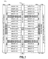
- the circuit 100 may comprise a first number of groups (e.g., GROUP 0W-15W), a second number of groups (e.g., GROUP 0E-15E) and a control circuit-113.
- the control circuit 113 may be implemented, in one example, as an address skew self-timed address transition detection (ATD) path (to be described in detail in connection with FIGS. 8(a)-8(b), FIG. 9 and FIG.10).
- ATD address skew self-timed address transition detection
- the circuit 100 may further comprise a block decoder 112, a row decoder 118, a row decoder 120, an I/O control block (or circuit) 124 and an I/O control block (or circuit) 125.
- the ATD path 113 may comprise a bitline equalization block (or circuit) 114, a bitline equalization block (or circuit) 116 and an address transition detection combination ATDMID circuit 122.
- the I/O control circuits 124 and 125 may comprise various circuits such as encoders, input buffers, address transition detection combination circuits, etc., to meet the criteria of a particular implementation.
- the row decoder 118 and the row decoder 120 are shown implemented between the GROUP 7W and the GROUP 8W, and the GROUP 7E and the GROUP 8E, respectively.
- the address transition detection combination circuit 122 (to be described in more detail in connection with FIG. 7) is shown implemented between the row decoder 118 and the row decoder 120.
- the bitline equalization circuits 114 and 116 are shown implemented above and below the address transition detection circuit decoder 122.
- the address transition detection circuit decoder 122 may control the bitline equalization circuits 114 and 116 using a single address transition signal (e.g., ATDG to be described in detail in conjunction with FIG. 10).
- the uniqueness of the bitline equalization circuits 114 and 116 may minimize rail-to-rail switching within the circuit 100.
- the circuit 100 may also comprise a number of redundant rows 126a-126n, a first plurality of redundant blocks 128a-128n and a second plurality of redundant blocks 130a-130n.
- the redundant blocks 128a-128n and 130a-130n may be implemented to replace a defective block within the circuit 100.
- the defective block may be electrically disconnected with one or more fuses (not shown) or other non-fuse alternative (for example, U.S. Serial No. 08/741,953).
- the redundant blocks 128a-128nand 130a-130n may only be activated when accessed in order to conserve power.
- a block power supply (e.g., Vccx) of the defective block may be disconnected from the supply voltage Vcc to eliminate additional current consumption in a stand-by mode. The replacement of the defective block may ensure the functionality of the circuit 100.
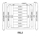
- FIG. 2 a block diagram of an exemplary block (e.g., GROUP 0) is shown.
- the GROUP 0 may comprise an output data multiplexer 140, an output data multiplexer 142, a local bus 144 and a local bus 146.
- the GROUP 0 may communicate to other devices (not shown) through a global bus 148 and a global bus 150.
- the bus 144 and the bus 146 may be implemented as single-ended local Q buses or other bus types in order to meet the criteria of a particular implementation.
- the global buses 148 and 150 may be implemented as single-ended global Q buses or other bus types in order to meet the criteria of a particular implementation.
- the GROUP 0 is shown implementing a number of blocks (e.g., BLOCKO-BLOCK7). While eight blocks are shown, the particular number of blocks may be adjusted accordingly to meet the design criteria of a particular implementation.
- the output data multiplexers 140 and 142 may multiplex data from the single-ended local Q bus to the single-ended global Q buses 148 and 150. The data is generally fed back through the single-ended global Q buses 148 and 150 to the other local buses of unaccessed blocks (not shown). The feedback of the data may help to avoid glitching of the data output path while selecting a new GROUP, as described in the referenced co-pending application.
- the BLOCK0 and the BLOCK1 generally comprise a bitline equalization path 150 and a driver block (or circuit) 152.
- the BLOCK0 and BLOCK1 may communicate through the single-ended Q logic bus 144.
- the Q logic bus may be common to, in one example, a group of 8 blocks.
- the BLOCK0 and BLOCK1 may communicate through the single ended Q logic bus 146.
- the driver circuit 152 may select the active block.
- the bitline equalization path 150 may comprise a bitline equalization block (or circuit) 154, a bitline equalization block (or circuit) 156 and a control block (or circuit) 158.
- the BLOCK0 and the BLOCK1 may each be interdigitated (e.g., able to be alternatively accessed from two sides) with respect to the bus 144 and the bus 146.
- the blocks BLOCK0 and BLOCK 1 are generally organized in a row fashion, without the implementation of column circuitry (e.g., column decoders, etc.). Since the bitline equalization circuits 154 and 156 are implemented within the blocks BLOCK0 and BLOCK1, respectively (as compared with conventional equalization circuits that are implemented in the periphery), a reduction in power may be achieved.
- the block BLOCK0 generally comprises a first number of cell columns (e.g., I/Ol'-I/016'), a bitline equalization circuit 156, a read/write block (or circuit) 166, a read/write block (or circuit) 168 and a driver 170.
- the block BLOCK1 generally comprises a second number of cell columns (e.g., I/O 1-I/O 16), a read/write block (or circuit) 160, a read/write block (or circuit) 162 and a driver 164.
- the driver 164 and the driver 170 may be implemented as a sub-wordline drivers or other driver types in order to meet the criteria of a particular implementation.
- a local sense amplifier (not shown) may be implemented in each block of first and second number of groups GROUPOW-15W and GROUPOE-15E. Furthermore, the local sense amplifiers may be implemented for each cell column (bitlines pair) of each block. The local sense amplifiers may drive the single-ended local Q buses 144 and 146.
- the blocks BLOCK0 and BLOCK1 are generally connected to the read/write circuits 160, 162, 166 and 168 through a number of bitlines.
- the wordlines are generally implemented as short sub-wordlines (e.g., a wordline connected to a limited number of memory cells).
- the blocks BLOCK0 and BLOCK1 may each be interdigitated (e.g., able to be alternatively accessed from both sides) with respect to the bus 144 and the bus 146.
- a small number of cells being selected within each block BLOCKO-7 of the first and second number of groups GROUPOW-15W and GROUPOE-15E may further reduce power consumption.
- bitline equalization circuit 114 an example of a bitline equalization circuit 114 is shown.
- the bitline equalization circuit 116 may be similar to the bitline equalization circuit 114.
- the bitline equalization circuit 114 is generally implemented between a bitline (e.g., BL) and a bitline bar (e.g., BLB).
- the equalization circuit 114 may be implemented with cross-coupled static bitline loads.
- the transistors 192 and 180 are generally cross-coupled to eliminate (or reduce) current consumption.
- the bitline equalization circuit 114 generally receives an equalization signal (e.g., EQB) at an input 180, the bitline BL at an input 182, the bitline bar BLB at an input 184 and a block current voltage (e.g., Vccx) at an input 186.
- the signal EQB may be an address transition detection signal (e.g., ATDBG) and/or a block enable signal (e.g., BLKSA) (not shown).
- the bitline equalization circuit 114 may present an equalized bitline (e.g., BL) at an output 182.
- the bitline equalization circuit 114 may present an equalized bitline bar (e.g., BLB) at an output 184.
- the bitline equalization circuit may present the equalized bitlines BL and BLB in response to the bitline BL, the bitline bar BLB, the signal EQB and the source block voltage Vccx.
- Reading and writing of data by the circuit 100 may be accomplished according to the signal EQB.
- the signal EQB may cause the bitline equalization circuits 114 and 116 to equalize the bitline BL and the bitline bar BLB during a pulse of a predetermined length (e.g., p). The length of pulse p, may be determined by the signal EQB.
- the equalized bitline BL and the equalized bitline bar BLB may connect to the memory cells of the addressed block from BLOCKO-BLOCK7 of the first and second number of groups GROUPOW-15W and GROUP0E-15E.
- the bitline BL and bitline bar BLB may read and/or write.
- the bitline BL and the bitline bar BLB may be equalized to the block voltage Vccx after each address and/or data transition and at the end of each write cycle. After the read and/or write the bitline BL and bitline bar BLB are generally fully excurted. The excurted bitline BL and the excurted bitline bar BLB generally do not draw any further current. Additionally, the signal EQB generally is valid only in the active blocks within the first and second number of groups GROUPOW-15W and GROUPOE-15E, which may save current.
- the sense amplifier 192 may power up the block in response to a signal (e.g., BLKBFUSE).
- the sense amplifier 192 may further power up the redundant blocks 128a-128n and 130a-130n when accessed.
- the sense amplifier 192 may be implemented, in one example, for every cell column of the circuit 100 (e.g., in every bitline pair, the bitline BL and the bitline bar BLB).
- the address transition circuit 122 generally comprise a logic block (or circuit) 200, a logic block (or circuit) 202, a logic block (or circuit) 204, a logic block (or circuit) 206, a logic block (or circuit) 208, a logic block (or circuit) 210 and a center logic block (or circuit) 212.
- the logic blocks (or circuits) 200, 202, 204 and 206 may be implemented with gates (see FIGS. 8a and 8b) or any other type of circuits in order to meet the criteria of a particular implementation.
- Each logic block (or circuit) 200, 202, 204 and 206 may comprise a combination block (or circuit) 201 a-201n and a combination block (or circuit) 203a-203n.
- the combination circuits 201a-201n and 203a-203n may be implemented as atdcomb circuits, dtdcomb circuits, or any other type of circuit in order to meet the criteria of a particular implementation.
- the logic block 200 may present a signal (e.g, ATD1') at an output 213 and a signal (e.g., DTD1') at an output 215.
- the atdcomb circuit 201 a may present the signal ATD1' in response to a plurality of signals (e.g., ADDRESS TRANSITION DETECT) received at an input 214 of the circuit 200.
- the dtdcomb circuit 203 may present the signal DTD1' in response to a plurality of signals (e.g., DTD1) received at an input 216.
- the circuit 202 may present a signal (e.g, ATD2') at an output 217 and a signal (e.g., DTD2') at an output 219.
- the atdcomb circuit 201b may present the signal ATD2' in response to one or more signals (e.g, ATD2) received at an input 218 of the circuit 202.
- the dtdcomb 203b may present the signal DTD2' in response to a plurality of signals (e.g., DTD2) received at an input 220 of the circuit 202.
- the signal ATD1', the signal DTD1', the signal ATD2', the signal DTD2', a control signal (e.g., CEW) and a signal (e.g., ATDE) may be presented to the logic circuit 208 at a number of inputs 222a-222n.
- the logic circuit 208 may be implemented as a west control logic circuit (e.g., a circuit that may control the west most blocks) or other type of logic circuit in order to meet the criteria of a particular implementation.
- the west control logic circuit 208 may present a signal (e.g., ATDW) at an output 224 and a signal (e.g., ATDBW) at an output 226.
- the circuit 204 may present a signal (e.g, ATD3') at an output 227 and a signal (e.g., DTD3') at an output 229.
- the atdcomb circuit 201 c may present the signal ATD3' in response to one or more signals (e.g, ATD3) received at an input 228 of the circuit 204.
- the dtdcomb circuit 203c may present the signal DTD3' in response to one or more signals (e.g., DTD3) received at an input 230 of the circuit 204.
- the circuit 206 may present a signal (e.g, ATD4') at an output 231 and a signal (e.g., DTD4') at an output 233.
- the atdcomb circuit 201n may present the signal ATD4' in response to one or more signals (e.g, ATD4) received at an input 232 of the circuit 206.
- the dtdcomb circuit 203n may present the signal DTD4' in response to a plurality of signals (e.g., DTD4) received at an input 234 of the circuit 206.
- the signals ATD1-ATD4 and the signals DTD1-DTD4 are generally generated by rail-to-rail switching of address or data inputs in the circuit 100.
- the signal ATD3', the signal DTD3', the signal ATD4', the signal DTD4', a control signal (e.g., CEE) and the signal ATDW may be presented to the logic circuit 210 at a number of inputs 236a-236n.
- the logic circuit 210 may be implemented as a east control logic circuit (e.g., a logic circuit that may control the east most blocks) or other type of logic circuit in order to meet the criteria of a particular implementation.
- the east control logic circuit 210 may present the signal ATDE at an output 238 and a signal (e.g., ATDBE) at an output 240.
- the signal ATDW and the signal ATDE may be presented to the center logic circuit 212 at an input 242 and 244, respectively.
- the center logic circuit 212 may present the signal ATDG at an output 246 in response to the signal ATDW and the signal ATDE.
- the signal ATDG may drive the bitline equalization circuits 114 and 116 (shown in FIG. 1). By using a single signal ATDG, the circuit 100 may save current by minimizing the number of bitlines that may switch rail-to-rail.
- the signal ATDBW and the signal ATDBE may be used in conjunction with the signal BLKSA in order to generate the equalization signal EQB.
- FIGS. 8(a)-8(b) examples of circuits that may be used to implement the atdcomb circuits 201a-201n and/or dtdcomb circuits 203a-203n of FIG. 7 are shown.
- the circuit of FIG. 8(a) may be the atdcomb circuit 201a.
- the atdcomb circuit 201a may present the signal ATD1' at an output 250 in response to the plurality of signals ADDRESS TRANSITION DETECT received at an input 252.
- the atdcomb circuit 201a may comprise a number of gates 260a-260n.
- the gates 260a-260n may be connected between the input 252 and the output 250.
- the gates 260a-260n may be implemented, in one example, as NOR gates and NAND gates. However, other type of gate configurations may be implemented in order to meet the criteria of a particular implementation.
- the implementation of the logic gates 260a-260n within the atdcomb circuits 201a-201n and the dtdcombs 203a-203n may prevent crowbar conditions in the circuit 100.
- the circuit of FIG. 8(b) shows a supplementary atd/dtdcomb circuit 270.
- the atd/dtdcomb circuit 270 may present a signal (e.g., ATD/DTD) at an output 272.
- the atd/dtdcomb circuit 270 may present the signal ATD/DTD in response to a number of signal (e.g., Na-Nn) received at a number of inputs 274a-274n.
- the atd/dtdcomb circuit 270 may comprise a number of inverters 276a-276n.
- the inverters 276c-276n may be connected between the inputs 274a-274n and a number of transistors 277a-277n.
- the source and drain connections of transistors 277a-277n may be serially connected between the inverters 276a-276b and ground.
- a number of transistors 279a-279n may also be connected between the inverters 276a-276b and ground.
- the drain terminals of the transistors 279a-279n may be coupled together.
- the source terminals of the transistors 279a-279n may be coupled to ground.
- the drain terminal of the transistor 279a may present the signal ATD/DTD at the output 272, through an inverter 281.
- the atd/dtdcomb circuit 270 may be allow for a larger number of input signals than the atdcomb circuit 201a of FIG. 8(a).
- the west control logic circuit may present the signal ADTW at the output 224 and the signal ATDBW at the output 226.
- the west control logic circuit 208 may present the signal ATDW and the signal ATDBW in response to a number of signals received at the inputs 222a-222n.
- the west control logic circuit 208 may receive the control signal CEW at the input 222a, the signal ATDE at the input 222b, the signal ATD1' at the input 222c, the signal ATD2' at the input 222d, the signal DTD1' at the input 222e and the signal DTD2' at the input 222n.
- the west control logic circuit 208 may comprise a number of gates 278a-278n and a number of inverters 280a-280n.
- the gates 278a-278n and the inverters 280a-280n may be coupled between the inputs 222a-222n and the outputs 224 and 226.
- the east control logic 210 may be similar to the west control logic circuit 208.
- the east control logic circuit 210 may present the signal ADTE at the output 238 and the signal ATDBE at the output 240.
- the east control logic circuit 210 may present the signal ATDE and the signal ATDBE in response to a number of signals received at the inputs 236a-236n.
- the east control logic circuit 210 may receive the control signal CEE at the input 236a, the signal ATDW at the input 236b, the signal ATD3' at the input 236c, the signal ATD4' at the input 236d, the signal DTD3' at the input 236e and the signal DTD4' at the input 236n.
- the center logic circuit 212 may present the signal ATDG at the output 246 in response to the signal ATDW received at the input 242 and the signal ATDE received at the input 244.
- the center logic circuit 212 may comprise a gate 290, an inverter 292 and an inverter 294.
- the gate 290 may be implemented, in one example, as a NOR gate. However, other types of logic gates may be implemented in order to meet the criteria of a particular implementation.
- the gate 290 may receive the signal ATDE at an input P and the signal ATDW at an input N.
- the inverters 292 and 294 may be connected between the gate 290 and the output 246.
- the implementation of the logic gates within the ATD path may prevent crowbar conditions in the circuit 100 that may minimize DC current consumption.
- the proposed architecture minimizes the DC and the AC power used in the circuit 100.
- the circuit 100 may maximize the advantages of two different approaches.
- the first approach may minimize or eliminate the DC current consumption.
- the second approach may minimize the AC current consumption.
- To achieve a minimal DC consumption a variety of new circuits were implemented.
- To reduce the AC current consumption the total capacitance switching rail-to-rail is generally minimized. Additionally, avoiding unnecessary switching may also reduce AC current consumption.
- the circuit 100 may implemented as a 2-Meg memory.
- the 2-Meg memory 100 may have a single ATD equalization signal ATDG that may control the bitline equalization circuits 114 and 116.
- the circuit 100 may be implemented as a 4-Meg memory.
- the 4-Meg memory 100 may implement two ATD equalization signals situated at 1/3 and 2/3 of the array. The two ATD equalization signals may be implemented due to increased length of the bitlines (which are two times longer). Additional size memory devices may also be implemented with similar numbers of ATD circuits.
- the circuit 100 may consume essentially zero DC current by implementing (i) the zero stand-by current input buffers, (ii) the cross-coupled static bitline loads BL and BLB, (iii) the sense amplifiers powered down by rail-to-rail excurting bitlines BL and BLB, and/or (iv) the gate-based address skew self-timed ATD path 113 that may avoid crowbarring conditions.
- the circuit 100 may minimize AC current by (i) organizing the first and second number of groups GROUP0W-15W and GROUP0E-15E in only blocks and rows, with no column address being used (as shown in FIG. 1), (ii) eliminating column address lines and circuitry for turn-on/equalization of the unaccessed columns and/or (iii) minimizing the number of cells active at a given time, for example, to 16 cells per block.
- TABLE 1 illustrates the power savings that the present invention may provide: TABLE 1 Circuit Icc (mA) Regular SRAM Icc (mA) Low Power SRAM Observations Row path 4.14 1.61
- AC single ended busses
- DC zero stand-by current input buffers
- AC single ended busses, only 16 cells per block active at a time
- DC zero stand-by current input buffers
- AC no predecoders, single ended busses, only 16 cells per block active at a time
- DC zero stand-by current input buffers, address skew self-timed ATD path, single ATD line placed in the middle of the array
- AC only 16 cells active at a time
- DC cross-coupled static bitline loads
- DC sense amplifier powered down by rail-to
- the cell-like subword line drivers 164 and 166 may be implemented inside the first and second number of groups GROUP0W-15W and GROUP0E-15E, respectively.
- a sub-wordline driver may be implemented for each row in each block BLOCK0-7 of the first and second number of groups GROUPOW-15W and GROUPOE-15E.
- the single-ended buses 144, 146, 148 and 150 are generally used in the periphery for the block address path, the local and global data output paths and the data input path.
- Sense amplifiers 192 of FIG. 6 followed by a driver/circuit (now shown) may drive a single-ended local Q-bus 144 and/or 146.
- Data on the global Q data bus 148 and/or 150 may be fed back to the local Q buses on all deselected groups that may avoid glitching of the data output path while selecting a new group of the first and second number of groups GROUPOW-15W and/or GROUP0E-15E.
- the signal ATDG which drives the equalization circuitry 114 and 116, may be generated by circuitry placed in the middle of the circuit 100.
- the block current Vccx may be disconnected from the supply voltage Vcc to eliminate the defective block contribution to current consumption in stand-by mode.
- the present invention may be particularly applicable to battery-operated devices, such as cellular phones, pagers, notebooks/palmtop computers, etc.
Landscapes
- Engineering & Computer Science (AREA)
- Microelectronics & Electronic Packaging (AREA)
- Static Random-Access Memory (AREA)
- Input Circuits Of Receivers And Coupling Of Receivers And Audio Equipment (AREA)
- Electronic Switches (AREA)
- Channel Selection Circuits, Automatic Tuning Circuits (AREA)
- Power Sources (AREA)
Abstract
Description
- The present invention may relate to co-pending applications in US Serial No. 09/222,578 and US Serial No. 09/200,219; US Patent No. 5,872,464 and US Patent No. 5,828,614.
- The present invention relates to memory circuits generally and more particularly, to an architecture, method and/or circuit for implementing a low power memory.
- Conventional memory architectures includes features that waste DC and AC current consumption by one or more of the following (I) passive (no gain) static loads, (ii) large sub-wordlines, (iii) sub-wordline circuits not included in the memory array, (iv) row, column and block array partitions not included in the memory array, (v) double ended buses (address path, local and global data output path), (vi) equalization circuitry placed at one end of the memory array, (vii) address predecoders, and/or (viii) replaced defective blocks still connected to the source current.
- US Patent No. 5,126,973 describes a redundancy scheme for eliminating defects in a memory device. The memory device comprises an array of memory cells and row decoders and column decoders use the buffered address signals to select the desired memory cells and connect their contents to I/O buffers. EP-A-0814481 describes a memory device in which a voltage booster is provided for supplying a read voltage higher than the supply voltage. US Patent No. 5,323,360 describes a memory having a section of memory cells, which uses address transition detection (ATD) to generate the required timing signals.
- US Patent No. 5,828,614 wherein the preamble of
claim 1 is based describes a memory circuit comprising blocks of memory cells, each comprising an equalization circuit and read/write circuitry. The blocks of memory cells form an array, or group, of memory cells. - In accordance with the present invention, there is provided a circuit as defined by
claim 1. - Also in accordance with the present invention there is provided a method as defined by claim 20.
- The objects, features and advantages of the present invention include providing a memory that may (I) reduce and/or eliminate DC current consumption, (ii) minimize rail-to-rail switching capacitance, (iii) reduce the amount of rail-to-rail switching, and/or (iv) reduce AC current consumption,
- These and other objects, features and advantages of the present invention will be apparent from the following detailed description and the appended claims and drawings in which:
- FIG. 1 is a block diagram of a preferred embodiment of the present invention;
- FIG. 2 is a block diagram of a group of the circuit of FIG. 1;
- FIG. 3 is a block diagram of a block configuration of the circuit of FIG. 2;
- FIG. 4 is a more detailed block diagram of a block configuration of the circuit of FIG. 3;
- FIG. 5 is a diagram of a bitline equalization circuit of FIG. 1;
- FIG. 6 is a diagram of a sense amplifier that may be used with the present invention;
- FIG. 7 is a detailed block diagram of an address transition detection combination circuit of FIG. 1;
- FIGS. 8(a)-8(b) are detailed circuit diagrams of the circuit of FIG. 7;
- FIG. 9 is a detailed circuit diagram of a control circuit of FIG. 7; and
- FIG. 10 is a detailed circuit diagram of another control circuit of FIG. 7.
- The present invention is an architecture that may minimize power consumption in a memory device by eliminating or reducing the DC current consumption and reducing the AC current consumption. To eliminate the DC power consumption, the present invention may implement (i) zero stand-by current input buffers as described in co-pending application Serial No. 09/222,578, (ii) cross-coupled static bitline loads, (iii) a sense amplifier powered down by rail-to-rail excurting bitlines and/or (iv) an address skew self-timed address transition detection (ATD) path that may avoid crowbarring conditions.
- To reduce the AC current consumption, the present invention may implement (i) a memory array organized in only blocks and rows (e.g., no column addresses used), (ii) single-ended buses in the periphery of the memory array and/or (iii) a single ATD equalization line that may drive equalization circuitry implemented in the middle of the memory array. The present invention may (i) eliminate predecoders in the address path, (ii) implement, in one example, only 16 cells per block that may be activated during access to the memory array, (iii) local amplifiers (e.g., one per bitline pair) that may drive single-ended local Q-buses, (iv) global to local output feedback for the unaccessed blocks and/or (v) blocks that may be powered down when defective and/or (vi) redundant blocks powered down when not in use.
- Referring to FIG. 1, a block diagram of a
circuit 100 is shown in accordance with a preferred embodiment of the invention. Thecircuit 100 may comprise a first number of groups (e.g., GROUP 0W-15W), a second number of groups (e.g., GROUP 0E-15E) and a control circuit-113. Thecontrol circuit 113 may be implemented, in one example, as an address skew self-timed address transition detection (ATD) path (to be described in detail in connection with FIGS. 8(a)-8(b), FIG. 9 and FIG.10). Thecircuit 100 may further comprise a block decoder 112, arow decoder 118, arow decoder 120, an I/O control block (or circuit) 124 and an I/O control block (or circuit) 125. TheATD path 113 may comprise a bitline equalization block (or circuit) 114, a bitline equalization block (or circuit) 116 and an address transition detectioncombination ATDMID circuit 122. The I/O control circuits 124 and 125 may comprise various circuits such as encoders, input buffers, address transition detection combination circuits, etc., to meet the criteria of a particular implementation. - The
row decoder 118 and therow decoder 120 are shown implemented between the GROUP 7W and the GROUP 8W, and the GROUP 7E and the GROUP 8E, respectively. The address transition detection combination circuit 122 (to be described in more detail in connection with FIG. 7) is shown implemented between therow decoder 118 and therow decoder 120. Thebitline equalization circuits detection circuit decoder 122. The address transitiondetection circuit decoder 122 may control thebitline equalization circuits bitline equalization circuits circuit 100. - The
circuit 100 may also comprise a number ofredundant rows 126a-126n, a first plurality ofredundant blocks 128a-128n and a second plurality ofredundant blocks 130a-130n. Theredundant blocks 128a-128n and 130a-130n may be implemented to replace a defective block within thecircuit 100. The defective block may be electrically disconnected with one or more fuses (not shown) or other non-fuse alternative (for example, U.S. Serial No. 08/741,953). - The
redundant blocks 128a-128nand 130a-130n may only be activated when accessed in order to conserve power. A block power supply (e.g., Vccx) of the defective block may be disconnected from the supply voltage Vcc to eliminate additional current consumption in a stand-by mode. The replacement of the defective block may ensure the functionality of thecircuit 100. - Referring to FIG. 2, a block diagram of an exemplary block (e.g., GROUP 0) is shown. Each of the first and second number of groups GROUP0-15 and may have similar components and/or function as the
GROUP 0 described in connection with FIG. 2. TheGROUP 0 may comprise anoutput data multiplexer 140, anoutput data multiplexer 142, alocal bus 144 and alocal bus 146. TheGROUP 0 may communicate to other devices (not shown) through aglobal bus 148 and aglobal bus 150. Thebus 144 and thebus 146 may be implemented as single-ended local Q buses or other bus types in order to meet the criteria of a particular implementation. Additionally, theglobal buses - The
GROUP 0 is shown implementing a number of blocks (e.g., BLOCKO-BLOCK7). While eight blocks are shown, the particular number of blocks may be adjusted accordingly to meet the design criteria of a particular implementation. Theoutput data multiplexers global Q buses global Q buses - Referring to FIG. 3 a block diagram of the BLOCK0 and BLOCK1 of FIG. 2 is shown. The BLOCK0 and the BLOCK1 generally comprise a
bitline equalization path 150 and a driver block (or circuit) 152. The BLOCK0 and BLOCK1 may communicate through the single-endedQ logic bus 144. The Q logic bus may be common to, in one example, a group of 8 blocks. Additionally, the BLOCK0 and BLOCK1 may communicate through the single endedQ logic bus 146. Thedriver circuit 152 may select the active block. - The
bitline equalization path 150 may comprise a bitline equalization block (or circuit) 154, a bitline equalization block (or circuit) 156 and a control block (or circuit) 158. The BLOCK0 and the BLOCK1 may each be interdigitated (e.g., able to be alternatively accessed from two sides) with respect to thebus 144 and thebus 146. - The blocks BLOCK0 and
BLOCK 1 are generally organized in a row fashion, without the implementation of column circuitry (e.g., column decoders, etc.). Since the bitline equalization circuits 154 and 156 are implemented within the blocks BLOCK0 and BLOCK1, respectively (as compared with conventional equalization circuits that are implemented in the periphery), a reduction in power may be achieved. - Referring to FIG. 4, a circuit diagram of the blocks BLOCK0 and BLOCK1 of FIG. 3 is shown. The block BLOCK0 generally comprises a first number of cell columns (e.g., I/Ol'-I/016'), a bitline equalization circuit 156, a read/write block (or circuit) 166, a read/write block (or circuit) 168 and a
driver 170. The block BLOCK1 generally comprises a second number of cell columns (e.g., I/O 1-I/O 16), a read/write block (or circuit) 160, a read/write block (or circuit) 162 and adriver 164. Thedriver 164 and thedriver 170 may be implemented as a sub-wordline drivers or other driver types in order to meet the criteria of a particular implementation. A local sense amplifier (not shown) may be implemented in each block of first and second number of groups GROUPOW-15W and GROUPOE-15E. Furthermore, the local sense amplifiers may be implemented for each cell column (bitlines pair) of each block. The local sense amplifiers may drive the single-endedlocal Q buses - The blocks BLOCK0 and BLOCK1 are generally connected to the read/
write circuits bus 144 and thebus 146. A small number of cells being selected within each block BLOCKO-7 of the first and second number of groups GROUPOW-15W and GROUPOE-15E may further reduce power consumption. - Referring to FIG. 5, an example of a
bitline equalization circuit 114 is shown. Thebitline equalization circuit 116 may be similar to thebitline equalization circuit 114. Thebitline equalization circuit 114 is generally implemented between a bitline (e.g., BL) and a bitline bar (e.g., BLB). Theequalization circuit 114 may be implemented with cross-coupled static bitline loads. Thetransistors - The
bitline equalization circuit 114 generally receives an equalization signal (e.g., EQB) at aninput 180, the bitline BL at aninput 182, the bitline bar BLB at aninput 184 and a block current voltage (e.g., Vccx) at aninput 186. The signal EQB may be an address transition detection signal (e.g., ATDBG) and/or a block enable signal (e.g., BLKSA) (not shown). Thebitline equalization circuit 114 may present an equalized bitline (e.g., BL) at anoutput 182. Thebitline equalization circuit 114 may present an equalized bitline bar (e.g., BLB) at anoutput 184. The bitline equalization circuit may present the equalized bitlines BL and BLB in response to the bitline BL, the bitline bar BLB, the signal EQB and the source block voltage Vccx. - Reading and writing of data by the
circuit 100 may be accomplished according to the signal EQB. The signal EQB may cause thebitline equalization circuits - Referring to FIG. 6, an example of a
sense amplifier 192 that may be implemented with the present invention is shown. Thesense amplifier 192 may power up the block in response to a signal (e.g., BLKBFUSE). Thesense amplifier 192 may further power up theredundant blocks 128a-128n and 130a-130n when accessed. Thesense amplifier 192 may be implemented, in one example, for every cell column of the circuit 100 (e.g., in every bitline pair, the bitline BL and the bitline bar BLB). - Referring to FIG. 7, an example of an address transition detection (ATD)
path circuit 122 is shown. Theaddress transition circuit 122 generally comprise a logic block (or circuit) 200, a logic block (or circuit) 202, a logic block (or circuit) 204, a logic block (or circuit) 206, a logic block (or circuit) 208, a logic block (or circuit) 210 and a center logic block (or circuit) 212. The logic blocks (or circuits) 200, 202, 204 and 206 may be implemented with gates (see FIGS. 8a and 8b) or any other type of circuits in order to meet the criteria of a particular implementation. Each logic block (or circuit) 200, 202, 204 and 206 may comprise a combination block (or circuit) 201 a-201n and a combination block (or circuit) 203a-203n. Thecombination circuits 201a-201n and 203a-203n may be implemented as atdcomb circuits, dtdcomb circuits, or any other type of circuit in order to meet the criteria of a particular implementation. - The
logic block 200 may present a signal (e.g, ATD1') at anoutput 213 and a signal (e.g., DTD1') at anoutput 215. Theatdcomb circuit 201 a may present the signal ATD1' in response to a plurality of signals (e.g., ADDRESS TRANSITION DETECT) received at an input 214 of thecircuit 200. The dtdcomb circuit 203 may present the signal DTD1' in response to a plurality of signals (e.g., DTD1) received at an input 216. - The
circuit 202 may present a signal (e.g, ATD2') at anoutput 217 and a signal (e.g., DTD2') at anoutput 219. Theatdcomb circuit 201b may present the signal ATD2' in response to one or more signals (e.g, ATD2) received at an input 218 of thecircuit 202. Thedtdcomb 203b may present the signal DTD2' in response to a plurality of signals (e.g., DTD2) received at aninput 220 of thecircuit 202. - The signal ATD1', the signal DTD1', the signal ATD2', the signal DTD2', a control signal (e.g., CEW) and a signal (e.g., ATDE) may be presented to the
logic circuit 208 at a number ofinputs 222a-222n. Thelogic circuit 208 may be implemented as a west control logic circuit (e.g., a circuit that may control the west most blocks) or other type of logic circuit in order to meet the criteria of a particular implementation. The westcontrol logic circuit 208 may present a signal (e.g., ATDW) at anoutput 224 and a signal (e.g., ATDBW) at anoutput 226. - The
circuit 204 may present a signal (e.g, ATD3') at anoutput 227 and a signal (e.g., DTD3') at anoutput 229. Theatdcomb circuit 201 c may present the signal ATD3' in response to one or more signals (e.g, ATD3) received at an input 228 of thecircuit 204. Thedtdcomb circuit 203c may present the signal DTD3' in response to one or more signals (e.g., DTD3) received at aninput 230 of thecircuit 204. - The
circuit 206 may present a signal (e.g, ATD4') at anoutput 231 and a signal (e.g., DTD4') at anoutput 233. Theatdcomb circuit 201n may present the signal ATD4' in response to one or more signals (e.g, ATD4) received at aninput 232 of thecircuit 206. Thedtdcomb circuit 203n may present the signal DTD4' in response to a plurality of signals (e.g., DTD4) received at an input 234 of thecircuit 206. The signals ATD1-ATD4 and the signals DTD1-DTD4 are generally generated by rail-to-rail switching of address or data inputs in thecircuit 100. - The signal ATD3', the signal DTD3', the signal ATD4', the signal DTD4', a control signal (e.g., CEE) and the signal ATDW may be presented to the
logic circuit 210 at a number ofinputs 236a-236n. Thelogic circuit 210 may be implemented as a east control logic circuit (e.g., a logic circuit that may control the east most blocks) or other type of logic circuit in order to meet the criteria of a particular implementation. The eastcontrol logic circuit 210 may present the signal ATDE at anoutput 238 and a signal (e.g., ATDBE) at anoutput 240. - The signal ATDW and the signal ATDE may be presented to the
center logic circuit 212 at aninput center logic circuit 212 may present the signal ATDG at anoutput 246 in response to the signal ATDW and the signal ATDE. The signal ATDG may drive thebitline equalization circuits 114 and 116 (shown in FIG. 1). By using a single signal ATDG, thecircuit 100 may save current by minimizing the number of bitlines that may switch rail-to-rail. The signal ATDBW and the signal ATDBE may be used in conjunction with the signal BLKSA in order to generate the equalization signal EQB. - Referring to FIGS. 8(a)-8(b), examples of circuits that may be used to implement the
atdcomb circuits 201a-201n and/ordtdcomb circuits 203a-203n of FIG. 7 are shown. In one example, the circuit of FIG. 8(a) may be theatdcomb circuit 201a. Theatdcomb circuit 201a may present the signal ATD1' at an output 250 in response to the plurality of signals ADDRESS TRANSITION DETECT received at aninput 252. Theatdcomb circuit 201a may comprise a number ofgates 260a-260n. Thegates 260a-260n may be connected between theinput 252 and the output 250. Thegates 260a-260n may be implemented, in one example, as NOR gates and NAND gates. However, other type of gate configurations may be implemented in order to meet the criteria of a particular implementation. The implementation of thelogic gates 260a-260n within theatdcomb circuits 201a-201n and the dtdcombs 203a-203n may prevent crowbar conditions in thecircuit 100. - The circuit of FIG. 8(b) shows a supplementary atd/
dtdcomb circuit 270. The atd/dtdcomb circuit 270 may present a signal (e.g., ATD/DTD) at an output 272. The atd/dtdcomb circuit 270 may present the signal ATD/DTD in response to a number of signal (e.g., Na-Nn) received at a number ofinputs 274a-274n. The atd/dtdcomb circuit 270 may comprise a number ofinverters 276a-276n. Theinverters 276c-276n may be connected between theinputs 274a-274n and a number oftransistors 277a-277n. The source and drain connections oftransistors 277a-277n may be serially connected between theinverters 276a-276b and ground. A number oftransistors 279a-279n may also be connected between theinverters 276a-276b and ground. The drain terminals of thetransistors 279a-279n may be coupled together. The source terminals of thetransistors 279a-279n may be coupled to ground. The drain terminal of thetransistor 279a may present the signal ATD/DTD at the output 272, through aninverter 281. The atd/dtdcomb circuit 270 may be allow for a larger number of input signals than theatdcomb circuit 201a of FIG. 8(a). - Referring to FIG. 9 a circuit diagram of the west control logic circuit of FIG.7 is shown. The west control logic circuit may present the signal ADTW at the
output 224 and the signal ATDBW at theoutput 226. The westcontrol logic circuit 208 may present the signal ATDW and the signal ATDBW in response to a number of signals received at theinputs 222a-222n. The westcontrol logic circuit 208 may receive the control signal CEW at theinput 222a, the signal ATDE at the input 222b, the signal ATD1' at theinput 222c, the signal ATD2' at the input 222d, the signal DTD1' at the input 222e and the signal DTD2' at theinput 222n. - The west
control logic circuit 208 may comprise a number ofgates 278a-278n and a number ofinverters 280a-280n. Thegates 278a-278n and theinverters 280a-280n may be coupled between theinputs 222a-222n and theoutputs east control logic 210 may be similar to the westcontrol logic circuit 208. The eastcontrol logic circuit 210 may present the signal ADTE at theoutput 238 and the signal ATDBE at theoutput 240. The eastcontrol logic circuit 210 may present the signal ATDE and the signal ATDBE in response to a number of signals received at theinputs 236a-236n. The eastcontrol logic circuit 210 may receive the control signal CEE at theinput 236a, the signal ATDW at the input 236b, the signal ATD3' at the input 236c, the signal ATD4' at the input 236d, the signal DTD3' at the input 236e and the signal DTD4' at theinput 236n. - Referring to FIG. 10 a circuit diagram of the
center logic circuit 212 of FIG. 7 is shown. Thecenter logic circuit 212 may present the signal ATDG at theoutput 246 in response to the signal ATDW received at theinput 242 and the signal ATDE received at theinput 244. Thecenter logic circuit 212 may comprise agate 290, aninverter 292 and aninverter 294. Thegate 290 may be implemented, in one example, as a NOR gate. However, other types of logic gates may be implemented in order to meet the criteria of a particular implementation. Thegate 290 may receive the signal ATDE at an input P and the signal ATDW at an input N. Theinverters gate 290 and theoutput 246. The implementation of the logic gates within the ATD path may prevent crowbar conditions in thecircuit 100 that may minimize DC current consumption. - The proposed architecture minimizes the DC and the AC power used in the
circuit 100. Thecircuit 100 may maximize the advantages of two different approaches. The first approach may minimize or eliminate the DC current consumption. The second approach may minimize the AC current consumption. To achieve a minimal DC consumption, a variety of new circuits were implemented. To reduce the AC current consumption, the total capacitance switching rail-to-rail is generally minimized. Additionally, avoiding unnecessary switching may also reduce AC current consumption. - In one example, the
circuit 100 may implemented as a 2-Meg memory. The 2-Meg memory 100 may have a single ATD equalization signal ATDG that may control thebitline equalization circuits circuit 100 may be implemented as a 4-Meg memory. The 4-Meg memory 100 may implement two ATD equalization signals situated at 1/3 and 2/3 of the array. The two ATD equalization signals may be implemented due to increased length of the bitlines (which are two times longer). Additional size memory devices may also be implemented with similar numbers of ATD circuits. - The
circuit 100 may consume essentially zero DC current by implementing (i) the zero stand-by current input buffers, (ii) the cross-coupled static bitline loads BL and BLB, (iii) the sense amplifiers powered down by rail-to-rail excurting bitlines BL and BLB, and/or (iv) the gate-based address skew self-timedATD path 113 that may avoid crowbarring conditions. - The
circuit 100 may minimize AC current by (i) organizing the first and second number of groups GROUP0W-15W and GROUP0E-15E in only blocks and rows, with no column address being used (as shown in FIG. 1), (ii) eliminating column address lines and circuitry for turn-on/equalization of the unaccessed columns and/or (iii) minimizing the number of cells active at a given time, for example, to 16 cells per block. - The following TABLE 1 illustrates the power savings that the present invention may provide:
TABLE 1 Circuit Icc (mA) Regular SRAM Icc (mA) Low Power SRAM Observations Row path 4.14 1.61 AC: single ended busses DC: zero stand-by current input buffers Block path 2.86 0.77 AC: single ended busses, only 16 cells per block active at a time DC: zero stand-by current input buffers Col path 3.08 N/A no columns used (no column address lines, no circuits of turn-on/equalization of the unaccessed columns) Address Total 10.08 2.38 AC: no predecoders, single ended busses, only 16 cells per block active at a time DC: zero stand-by current input buffers, address skew self-timed ATD path, single ATD line placed in the middle of the array Bitlines 16.17 0.94 AC: only 16 cells active at a time DC: cross-coupled static bitline loads Senseamps 12.17 0.91 DC: sense amplifier powered down by rail-to-rail excurting bitlines Q path 19.51 0.61 In regular SRAM, DC consumption during write + differential lines In Low Power: single-ended Q lines, global Q data is fed back to local Q lines on all deselected groups ICC total 62.81 9.43 - The cell-like
subword line drivers buses Sense amplifiers 192 of FIG. 6 followed by a driver/circuit (now shown) may drive a single-ended local Q-bus 144 and/or 146. Data on the globalQ data bus 148 and/or 150 may be fed back to the local Q buses on all deselected groups that may avoid glitching of the data output path while selecting a new group of the first and second number of groups GROUPOW-15W and/or GROUP0E-15E. The signal ATDG, which drives theequalization circuitry circuit 100. The block current Vccx may be disconnected from the supply voltage Vcc to eliminate the defective block contribution to current consumption in stand-by mode. - The present invention may be particularly applicable to battery-operated devices, such as cellular phones, pagers, notebooks/palmtop computers, etc.
- While the invention has been particularly shown and described with reference to the preferred embodiments thereof, it will be understood by those skilled in the art that various changes in form and details may be made without departing from the scope of the invention.
Claims (24)
- A circuit (100) comprising:a first and second bitline (BL, BLB) each configured to read and write data to one or more of a plurality of groups (OW-15W, OE-15E) of memory cells, said groups of memory cells comprising a plurality of blocks (Block 0-Block 7) and read/write circuitry (140, 142),said blocks (Block 0 - Block 7) are arranged in a column direction and each block comprising a bit line equalization circuit (154), characterized in that: said blocks are arranged between said read/write circuitry (140, 142) located at the periphery of the blocks (Block 0 - Block 7), and each block configured to arrange the equalization circuit in its middle, said blocks further being configured to comprise a control circuit (113) comprising a bit line equalization path (150), said bitline equalization path (150) comprising the bit line equalization circuit (154) in each block (Block 0 - Block 7).
- The circuit (100) according to claim 1, wherein each of said groups of memory cells is interdigitated.
- The circuit (100) according to claim 1 or 2, wherein each of said plurality of blocks comprises a plurality of short sub-wordlines.
- The circuit (100) according to claim 3, wherein each of said cells in said active group are active when said short sub-wordlines are active, without column addresses.
- The circuit (100) according to claim 1, wherein said control circuit further comprises a single address transition detection circuit (270) configured to decode said data to be read or written.
- The circuit (100) according to claim 1, wherein each block of said plurality of blocks comprises a sub-wordline driver (164,170) for each row.
- The circuit (100) according to claim 1, wherein said first and second bitlines (BL,BLB) have cross-coupled loads.
- The circuit (100) according to claim 1, further comprising one or more local buses (144,146) and one or more global buses (148,150), wherein each of said local buses (144,146) comprises one or more single-ended local Q buses and each of said global buses (148,150) comprises one or more single-ended global Q buses.
- The circuit (100) according to claim 1, wherein each block of said plurality of blocks comprises a plurality of said memory cells.
- The circuit (100) according to claim 9, where each bitline pair (BL, BLB) comprises a sense amplifier, wherein said each sense amplifier is configured to drive said one or more local buses.
- The circuit (100) according to claim 1, wherein said control circuit (113) is further configured to disconnect a defective block from a block power supply.
- The circuit (100) according to claim 11, wherein said control circuit (113) is further configured to replace said defective block with one or more redundant blocks that are active only when the said block is enabled.
- The circuit (100) according to claim 1, wherein said plurality of groups are organized in rows and blocks.
- The circuit (100) according to claim 1, wherein said control circuit (113) is configured to select said active group by means of a single address transition detection signal and one or more control signals.
- The circuit (100) according to claim 8, wherein said one or more global data buses (148,150) are configured to feed back data to said one or more local buses (144,146) of said groups that are deselected.
- The circuit (100) according to claim 8, where each of said first and second bitline pair (BL,BLB) comprises a sense amplifier, wherein said each sense amplifier is, configured to drive said one or more local buses (144,146).
- The circuit (100) according to claim 16, wherein said each sense amplifier is powered down by rail-to-rail escorting of said first and second bit line pair (BL,BLB).
- The circuit (100) according to claim 1, wherein said control circuit (113) is further configured to disconnect a defective block from a block power supply.
- The circuit (100) according to claim 18, wherein said control circuit (113) is further configured to replace said defective block with one or more redundant blocks that are active only when enabled.
- A method for reading and writing data to a plurality of memory cells comprising the steps of :(a) reading and writing to and/or from a selected group of a plurality of groups (OW-15W, OE-15E) of said memory cells, each of said groups comprising blocks (Block 0 - Block 7) of memory cells, using a first and a second bit line (BL,BLB);
characterized by the steps of:(b) selecting an active group of said plurality of groups in response to a single address transition detection signal, generated by a control circuit (113) within said group of memory cells, and reading and/or writing to/from said active group by way of read/write circuitry located at the periphery of said blocks (Block 0 - Block 7) and by way of an equalization path comprising equalization circuits each located in the middle of a respective block. - The method of claim 20, wherein said active group of memory cells is selected and additionally in response to the value of the address.
- The method according to claim 20, wherein (I) each group is organized in a plurality of rows and a plurality of blocks and/or (ii) each block of said plurality of blocks comprises a sub wordline driver for each row.
- The method according to claim 22, further comprising the step of(c) disconnecting a defective block of said plurality of blocks from a block power supply and replacing the defective block with a redundant block.
- The method according to claim 20, wherein each bit line pair (BL,BLB) comprises a sense amplifier.
Applications Claiming Priority (3)
| Application Number | Priority Date | Filing Date | Title |
|---|---|---|---|
| US398735 | 1982-07-15 | ||
| US09/398,735 US6163495A (en) | 1999-09-17 | 1999-09-17 | Architecture, method(s) and circuitry for low power memories |
| PCT/US2000/025374 WO2001020610A1 (en) | 1999-09-17 | 2000-09-15 | Architecture, method(s) and circuitry for low power memories |
Publications (3)
| Publication Number | Publication Date |
|---|---|
| EP1214713A1 EP1214713A1 (en) | 2002-06-19 |
| EP1214713A4 EP1214713A4 (en) | 2004-12-22 |
| EP1214713B1 true EP1214713B1 (en) | 2007-06-06 |
Family
ID=23576591
Family Applications (1)
| Application Number | Title | Priority Date | Filing Date |
|---|---|---|---|
| EP00963517A Expired - Lifetime EP1214713B1 (en) | 1999-09-17 | 2000-09-15 | Architecture, method(s) and circuitry for low power memories |
Country Status (10)
| Country | Link |
|---|---|
| US (3) | US6163495A (en) |
| EP (1) | EP1214713B1 (en) |
| JP (1) | JP5105680B2 (en) |
| KR (1) | KR100765157B1 (en) |
| AT (1) | ATE364228T1 (en) |
| AU (1) | AU7492100A (en) |
| CA (1) | CA2384862A1 (en) |
| DE (1) | DE60035115T2 (en) |
| IL (2) | IL148680A0 (en) |
| WO (1) | WO2001020610A1 (en) |
Families Citing this family (22)
| Publication number | Priority date | Publication date | Assignee | Title |
|---|---|---|---|---|
| US6163495A (en) | 1999-09-17 | 2000-12-19 | Cypress Semiconductor Corp. | Architecture, method(s) and circuitry for low power memories |
| US6530040B1 (en) * | 1999-09-22 | 2003-03-04 | Cypress Semiconductor Corp. | Parallel test in asynchronous memory with single-ended output path |
| US6417697B2 (en) | 2000-02-02 | 2002-07-09 | Broadcom Corporation | Circuit technique for high speed low power data transfer bus |
| US8164362B2 (en) * | 2000-02-02 | 2012-04-24 | Broadcom Corporation | Single-ended sense amplifier with sample-and-hold reference |
| US6411557B2 (en) | 2000-02-02 | 2002-06-25 | Broadcom Corporation | Memory architecture with single-port cell and dual-port (read and write) functionality |
| US6745354B2 (en) | 2000-02-02 | 2004-06-01 | Broadcom Corporation | Memory redundancy implementation |
| US6937538B2 (en) * | 2000-02-02 | 2005-08-30 | Broadcom Corporation | Asynchronously resettable decoder for a semiconductor memory |
| US6414899B2 (en) | 2000-02-02 | 2002-07-02 | Broadcom Corporation | Limited swing driver circuit |
| US7173867B2 (en) * | 2001-02-02 | 2007-02-06 | Broadcom Corporation | Memory redundancy circuit techniques |
| US6535025B2 (en) | 2000-02-02 | 2003-03-18 | Broadcom Corp. | Sense amplifier with offset cancellation and charge-share limited swing drivers |
| US6603712B2 (en) | 2000-02-02 | 2003-08-05 | Broadcom Corporation | High precision delay measurement circuit |
| US6611465B2 (en) | 2000-02-02 | 2003-08-26 | Broadcom Corporation | Diffusion replica delay circuit |
| US6492844B2 (en) | 2000-02-02 | 2002-12-10 | Broadcom Corporation | Single-ended sense amplifier with sample-and-hold reference |
| US6724681B2 (en) * | 2000-02-02 | 2004-04-20 | Broadcom Corporation | Asynchronously-resettable decoder with redundancy |
| US6714467B2 (en) * | 2002-03-19 | 2004-03-30 | Broadcom Corporation | Block redundancy implementation in heirarchical RAM's |
| KR100625294B1 (en) * | 2004-10-30 | 2006-09-18 | 주식회사 하이닉스반도체 | Power supply control circuit and control method of the power supply circuit |
| JP4917767B2 (en) * | 2005-07-01 | 2012-04-18 | パナソニック株式会社 | Semiconductor memory device |
| KR100700160B1 (en) * | 2005-08-23 | 2007-03-28 | 삼성전자주식회사 | Word line activation method of semiconductor memory device and semiconductor memory device |
| DE102007007566B4 (en) * | 2007-02-15 | 2012-08-23 | Qimonda Ag | Semiconductor device system, memory module, and method of operating a semiconductor device system |
| WO2011134079A1 (en) * | 2010-04-27 | 2011-11-03 | Mosaid Technologies Incorporated | Phase change memory array blocks with alternate selection |
| US8526227B2 (en) | 2010-06-23 | 2013-09-03 | Mosaid Technologies Incorporated | Phase change memory word line driver |
| US10316152B2 (en) | 2014-01-10 | 2019-06-11 | CommScope Connectivity Belgium BVBA | Thermoplastic gel compositions and their methods of making |
Family Cites Families (36)
| Publication number | Priority date | Publication date | Assignee | Title |
|---|---|---|---|---|
| JPH01178193A (en) * | 1988-01-07 | 1989-07-14 | Toshiba Corp | Semiconductor storage device |
| JPH01294295A (en) * | 1988-05-20 | 1989-11-28 | Fujitsu Ltd | Partial random access memory |
| JP2547615B2 (en) * | 1988-06-16 | 1996-10-23 | 三菱電機株式会社 | Read-only semiconductor memory device and semiconductor memory device |
| JP2805761B2 (en) * | 1988-08-29 | 1998-09-30 | 日本電気株式会社 | Static memory |
| US5349206A (en) * | 1988-11-10 | 1994-09-20 | Seiko Epson Corporation | Integrated memory circuit with high density load elements |
| JPH02247892A (en) * | 1989-03-20 | 1990-10-03 | Fujitsu Ltd | Dynamic random access memory |
| US4985639A (en) * | 1989-07-07 | 1991-01-15 | Hewlett-Packard Company | Logic edge timing generation |
| US5126973A (en) * | 1990-02-14 | 1992-06-30 | Texas Instruments Incorporated | Redundancy scheme for eliminating defects in a memory device |
| US5270975A (en) * | 1990-03-29 | 1993-12-14 | Texas Instruments Incorporated | Memory device having a non-uniform redundancy decoder arrangement |
| JPH0474384A (en) * | 1990-07-17 | 1992-03-09 | Toshiba Corp | Semiconductor integrated circuit device |
| JP2519593B2 (en) * | 1990-10-24 | 1996-07-31 | 三菱電機株式会社 | Semiconductor memory device |
| JPH04182988A (en) * | 1990-11-16 | 1992-06-30 | Hitachi Ltd | Semiconductor memory device |
| JPH06103599B2 (en) * | 1990-11-16 | 1994-12-14 | 三菱電機株式会社 | Semiconductor integrated circuit device |
| JPH0563525A (en) * | 1991-08-29 | 1993-03-12 | Nec Corp | Pulse width variable circuit |
| JPH05151797A (en) * | 1991-11-26 | 1993-06-18 | Nec Ic Microcomput Syst Ltd | Semiconductor integrated circuit |
| JP3605122B2 (en) * | 1991-12-13 | 2004-12-22 | テキサス インスツルメンツ インコーポレイテツド | Compensation circuit and method of compensating for delay |
| JPH05307899A (en) * | 1992-04-24 | 1993-11-19 | Samsung Electron Co Ltd | Semiconductor memory storage |
| US5264745A (en) * | 1992-08-28 | 1993-11-23 | Advanced Micro Devices, Inc. | Recovering phase and data from distorted duty cycles caused by ECL-to-CMOS translator |
| KR950004855B1 (en) * | 1992-10-30 | 1995-05-15 | 현대전자산업 주식회사 | Address transition detection circuit of semiconductor memory device |
| US5323360A (en) * | 1993-05-03 | 1994-06-21 | Motorola Inc. | Localized ATD summation for a memory |
| EP0713609B1 (en) * | 1993-08-13 | 2003-05-07 | Irvine Sensors Corporation | Stack of ic chips as substitute for single ic chip |
| US5696463A (en) * | 1993-11-02 | 1997-12-09 | Hyundai Electronics Industries Co., Ltd. | Address transition detecting circuit which generates constant pulse width signal |
| US5555529A (en) * | 1993-12-28 | 1996-09-10 | Intel Corporation | Power saving architecture for a cache memory |
| JPH08172169A (en) * | 1994-12-16 | 1996-07-02 | Toshiba Microelectron Corp | Semiconductor memory device |
| JPH08273363A (en) * | 1995-03-30 | 1996-10-18 | Nec Corp | Semiconductor memory |
| AU1752297A (en) * | 1996-01-24 | 1997-08-20 | Cypress Semiconductor Corp. | Interdigitated memory array |
| EP0814481B1 (en) * | 1996-06-18 | 2002-03-20 | STMicroelectronics S.r.l. | Low-supply-voltage nonvolatile memory device with voltage boosting |
| US5872464A (en) * | 1996-08-12 | 1999-02-16 | Cypress Semiconductor Corp. | Input buffer with stabilized trip points |
| US5968190A (en) | 1996-10-31 | 1999-10-19 | Cypress Semiconductor Corp. | Redundancy method and circuit for self-repairing memory arrays |
| KR100240418B1 (en) * | 1996-12-31 | 2000-03-02 | 윤종용 | Semiconductor read only memory and its read method |
| US5828614A (en) * | 1997-04-07 | 1998-10-27 | Cypress Semiconductor Corp. | Memory cell sensing method and circuitry for bit line equalization |
| JPH11195766A (en) * | 1997-10-31 | 1999-07-21 | Mitsubishi Electric Corp | Semiconductor integrated circuit device |
| US6118727A (en) | 1998-03-10 | 2000-09-12 | Cypress Semiconductor Corporation | Semiconductor memory with interdigitated array having bit line pairs accessible from either of two sides of the array |
| US6378008B1 (en) | 1998-11-25 | 2002-04-23 | Cypress Semiconductor Corporation | Output data path scheme in a memory device |
| US6323701B1 (en) | 1998-12-28 | 2001-11-27 | Cypress Semiconductor Corporation | Scheme for reducing leakage current in an input buffer |
| US6163495A (en) * | 1999-09-17 | 2000-12-19 | Cypress Semiconductor Corp. | Architecture, method(s) and circuitry for low power memories |
-
1999
- 1999-09-17 US US09/398,735 patent/US6163495A/en not_active Expired - Lifetime
-
2000
- 2000-09-15 KR KR1020027003582A patent/KR100765157B1/en not_active Expired - Fee Related
- 2000-09-15 JP JP2001524103A patent/JP5105680B2/en not_active Expired - Fee Related
- 2000-09-15 AT AT00963517T patent/ATE364228T1/en not_active IP Right Cessation
- 2000-09-15 AU AU74921/00A patent/AU7492100A/en not_active Abandoned
- 2000-09-15 DE DE60035115T patent/DE60035115T2/en not_active Expired - Lifetime
- 2000-09-15 EP EP00963517A patent/EP1214713B1/en not_active Expired - Lifetime
- 2000-09-15 WO PCT/US2000/025374 patent/WO2001020610A1/en not_active Ceased
- 2000-09-15 IL IL14868000A patent/IL148680A0/en active IP Right Grant
- 2000-09-15 CA CA002384862A patent/CA2384862A1/en not_active Abandoned
- 2000-11-22 US US09/721,324 patent/US6493283B1/en not_active Expired - Lifetime
-
2002
- 2002-03-13 IL IL148680A patent/IL148680A/en not_active IP Right Cessation
- 2002-07-19 US US10/199,560 patent/US6674682B2/en not_active Expired - Lifetime
Non-Patent Citations (1)
| Title |
|---|
| None * |
Also Published As
| Publication number | Publication date |
|---|---|
| JP2003509802A (en) | 2003-03-11 |
| ATE364228T1 (en) | 2007-06-15 |
| EP1214713A4 (en) | 2004-12-22 |
| IL148680A (en) | 2007-12-03 |
| IL148680A0 (en) | 2002-09-12 |
| EP1214713A1 (en) | 2002-06-19 |
| DE60035115T2 (en) | 2008-01-31 |
| DE60035115D1 (en) | 2007-07-19 |
| KR100765157B1 (en) | 2007-10-15 |
| CA2384862A1 (en) | 2001-03-22 |
| WO2001020610A1 (en) | 2001-03-22 |
| US6493283B1 (en) | 2002-12-10 |
| US6163495A (en) | 2000-12-19 |
| JP5105680B2 (en) | 2012-12-26 |
| KR20020035142A (en) | 2002-05-09 |
| US6674682B2 (en) | 2004-01-06 |
| US20020191470A1 (en) | 2002-12-19 |
| AU7492100A (en) | 2001-04-17 |
Similar Documents
| Publication | Publication Date | Title |
|---|---|---|
| US6163495A (en) | Architecture, method(s) and circuitry for low power memories | |
| EP0600184B1 (en) | Semiconductor memory device having dual word line structure | |
| US5982690A (en) | Static low-power differential sense amplifier circuits, systems and methods | |
| US5267197A (en) | Read/write memory having an improved write driver | |
| US7079426B2 (en) | Dynamic multi-Vcc scheme for SRAM cell stability control | |
| KR100368367B1 (en) | Semiconductor memory device | |
| US7505319B2 (en) | Method and apparatus for high efficiency redundancy scheme for multi-segment SRAM | |
| KR0164377B1 (en) | Sub-word line driver | |
| US5706231A (en) | Semiconductor memory device having a redundant memory cell | |
| EP0547919B1 (en) | A semiconductor memory with power-on reset control of disabled rows | |
| US5757689A (en) | Semiconductor memory activated by plurality of word lines on same row | |
| KR0145165B1 (en) | Redundant address decoder | |
| US6819623B2 (en) | Integrated circuit memory devices having efficient column select signal generation during normal and refresh modes of operation and methods of operating same | |
| EP0790619B1 (en) | Current limiting during block writes of memory circuits | |
| US6249464B1 (en) | Block redundancy in ultra low power memory circuits | |
| JP2003151295A (en) | Semiconductor device | |
| US6246631B1 (en) | Semiconductor memory device | |
| JP5289469B2 (en) | Method and apparatus for word line decoder layout | |
| US6487138B2 (en) | Semiconductor memory | |
| US6975548B2 (en) | Memory device having redundant memory cell | |
| US7193926B2 (en) | Memory device for reducing leakage current | |
| CA2246763C (en) | Improved redundancy selection circuit for semiconductor memories | |
| US6404700B1 (en) | Low power high density asynchronous memory architecture | |
| JPH0676595A (en) | Semiconductor memory | |
| US20040246771A1 (en) | Method of transferring data |
Legal Events
| Date | Code | Title | Description |
|---|---|---|---|
| PUAI | Public reference made under article 153(3) epc to a published international application that has entered the european phase |
Free format text: ORIGINAL CODE: 0009012 |
|
| 17P | Request for examination filed |
Effective date: 20020410 |
|
| AK | Designated contracting states |
Kind code of ref document: A1 Designated state(s): AT BE CH CY DE DK ES FI FR GB GR IE IT LI LU MC NL PT SE |
|
| AX | Request for extension of the european patent |
Free format text: AL;LT;LV;MK;RO;SI |
|
| A4 | Supplementary search report drawn up and despatched |
Effective date: 20041110 |
|
| RIC1 | Information provided on ipc code assigned before grant |
Ipc: 7G 11C 8/18 B Ipc: 7G 11C 7/12 B Ipc: 7G 11C 8/12 A |
|
| 17Q | First examination report despatched |
Effective date: 20050120 |
|
| 17Q | First examination report despatched |
Effective date: 20050120 |
|
| GRAP | Despatch of communication of intention to grant a patent |
Free format text: ORIGINAL CODE: EPIDOSNIGR1 |
|
| GRAS | Grant fee paid |
Free format text: ORIGINAL CODE: EPIDOSNIGR3 |
|
| GRAA | (expected) grant |
Free format text: ORIGINAL CODE: 0009210 |
|
| AK | Designated contracting states |
Kind code of ref document: B1 Designated state(s): AT BE CH CY DE DK ES FI FR GB GR IE IT LI LU MC NL PT SE |
|
| PG25 | Lapsed in a contracting state [announced via postgrant information from national office to epo] |
Ref country code: CH Free format text: LAPSE BECAUSE OF FAILURE TO SUBMIT A TRANSLATION OF THE DESCRIPTION OR TO PAY THE FEE WITHIN THE PRESCRIBED TIME-LIMIT Effective date: 20070606 Ref country code: LI Free format text: LAPSE BECAUSE OF FAILURE TO SUBMIT A TRANSLATION OF THE DESCRIPTION OR TO PAY THE FEE WITHIN THE PRESCRIBED TIME-LIMIT Effective date: 20070606 Ref country code: FI Free format text: LAPSE BECAUSE OF FAILURE TO SUBMIT A TRANSLATION OF THE DESCRIPTION OR TO PAY THE FEE WITHIN THE PRESCRIBED TIME-LIMIT Effective date: 20070606 |
|
| REG | Reference to a national code |
Ref country code: GB Ref legal event code: FG4D |
|
| REG | Reference to a national code |
Ref country code: CH Ref legal event code: EP |
|
| REG | Reference to a national code |
Ref country code: IE Ref legal event code: FG4D |
|
| REF | Corresponds to: |
Ref document number: 60035115 Country of ref document: DE Date of ref document: 20070719 Kind code of ref document: P |
|
| PG25 | Lapsed in a contracting state [announced via postgrant information from national office to epo] |
Ref country code: SE Free format text: LAPSE BECAUSE OF FAILURE TO SUBMIT A TRANSLATION OF THE DESCRIPTION OR TO PAY THE FEE WITHIN THE PRESCRIBED TIME-LIMIT Effective date: 20070906 |
|
| PG25 | Lapsed in a contracting state [announced via postgrant information from national office to epo] |
Ref country code: ES Free format text: LAPSE BECAUSE OF FAILURE TO SUBMIT A TRANSLATION OF THE DESCRIPTION OR TO PAY THE FEE WITHIN THE PRESCRIBED TIME-LIMIT Effective date: 20070917 |
|
| PG25 | Lapsed in a contracting state [announced via postgrant information from national office to epo] |
Ref country code: AT Free format text: LAPSE BECAUSE OF FAILURE TO SUBMIT A TRANSLATION OF THE DESCRIPTION OR TO PAY THE FEE WITHIN THE PRESCRIBED TIME-LIMIT Effective date: 20070606 |
|
| NLV1 | Nl: lapsed or annulled due to failure to fulfill the requirements of art. 29p and 29m of the patents act | ||
| ET | Fr: translation filed | ||
| REG | Reference to a national code |
Ref country code: CH Ref legal event code: PL |
|
| PG25 | Lapsed in a contracting state [announced via postgrant information from national office to epo] |
Ref country code: BE Free format text: LAPSE BECAUSE OF FAILURE TO SUBMIT A TRANSLATION OF THE DESCRIPTION OR TO PAY THE FEE WITHIN THE PRESCRIBED TIME-LIMIT Effective date: 20070606 |
|
| PG25 | Lapsed in a contracting state [announced via postgrant information from national office to epo] |
Ref country code: NL Free format text: LAPSE BECAUSE OF FAILURE TO SUBMIT A TRANSLATION OF THE DESCRIPTION OR TO PAY THE FEE WITHIN THE PRESCRIBED TIME-LIMIT Effective date: 20070606 Ref country code: PT Free format text: LAPSE BECAUSE OF FAILURE TO SUBMIT A TRANSLATION OF THE DESCRIPTION OR TO PAY THE FEE WITHIN THE PRESCRIBED TIME-LIMIT Effective date: 20071106 |
|
| PLBE | No opposition filed within time limit |
Free format text: ORIGINAL CODE: 0009261 |
|
| STAA | Information on the status of an ep patent application or granted ep patent |
Free format text: STATUS: NO OPPOSITION FILED WITHIN TIME LIMIT |
|
| PG25 | Lapsed in a contracting state [announced via postgrant information from national office to epo] |
Ref country code: GR Free format text: LAPSE BECAUSE OF FAILURE TO SUBMIT A TRANSLATION OF THE DESCRIPTION OR TO PAY THE FEE WITHIN THE PRESCRIBED TIME-LIMIT Effective date: 20070907 Ref country code: IT Free format text: LAPSE BECAUSE OF FAILURE TO SUBMIT A TRANSLATION OF THE DESCRIPTION OR TO PAY THE FEE WITHIN THE PRESCRIBED TIME-LIMIT Effective date: 20070606 Ref country code: DK Free format text: LAPSE BECAUSE OF FAILURE TO SUBMIT A TRANSLATION OF THE DESCRIPTION OR TO PAY THE FEE WITHIN THE PRESCRIBED TIME-LIMIT Effective date: 20070606 Ref country code: MC Free format text: LAPSE BECAUSE OF NON-PAYMENT OF DUE FEES Effective date: 20070930 |
|
| 26N | No opposition filed |
Effective date: 20080307 |
|
| PG25 | Lapsed in a contracting state [announced via postgrant information from national office to epo] |
Ref country code: IE Free format text: LAPSE BECAUSE OF NON-PAYMENT OF DUE FEES Effective date: 20070917 |
|
| REG | Reference to a national code |
Ref country code: GB Ref legal event code: 732E Free format text: REGISTERED BETWEEN 20090219 AND 20090225 |
|
| PG25 | Lapsed in a contracting state [announced via postgrant information from national office to epo] |
Ref country code: CY Free format text: LAPSE BECAUSE OF FAILURE TO SUBMIT A TRANSLATION OF THE DESCRIPTION OR TO PAY THE FEE WITHIN THE PRESCRIBED TIME-LIMIT Effective date: 20070606 |
|
| PG25 | Lapsed in a contracting state [announced via postgrant information from national office to epo] |
Ref country code: LU Free format text: LAPSE BECAUSE OF NON-PAYMENT OF DUE FEES Effective date: 20070915 |
|
| REG | Reference to a national code |
Ref country code: FR Ref legal event code: TP |
|
| REG | Reference to a national code |
Ref country code: FR Ref legal event code: PLFP Year of fee payment: 17 |
|
| REG | Reference to a national code |
Ref country code: FR Ref legal event code: PLFP Year of fee payment: 18 |
|
| REG | Reference to a national code |
Ref country code: FR Ref legal event code: PLFP Year of fee payment: 19 |
|
| PGFP | Annual fee paid to national office [announced via postgrant information from national office to epo] |
Ref country code: FR Payment date: 20180817 Year of fee payment: 19 Ref country code: DE Payment date: 20180815 Year of fee payment: 19 |
|
| PGFP | Annual fee paid to national office [announced via postgrant information from national office to epo] |
Ref country code: GB Payment date: 20180828 Year of fee payment: 19 |
|
| REG | Reference to a national code |
Ref country code: DE Ref legal event code: R119 Ref document number: 60035115 Country of ref document: DE |
|
| PG25 | Lapsed in a contracting state [announced via postgrant information from national office to epo] |
Ref country code: DE Free format text: LAPSE BECAUSE OF NON-PAYMENT OF DUE FEES Effective date: 20200401 |
|
| GBPC | Gb: european patent ceased through non-payment of renewal fee |
Effective date: 20190915 |
|
| PG25 | Lapsed in a contracting state [announced via postgrant information from national office to epo] |
Ref country code: FR Free format text: LAPSE BECAUSE OF NON-PAYMENT OF DUE FEES Effective date: 20190930 Ref country code: GB Free format text: LAPSE BECAUSE OF NON-PAYMENT OF DUE FEES Effective date: 20190915 |