EP1213907A2 - switched mode current feed methods for telephony subcriber loops - Google Patents
switched mode current feed methods for telephony subcriber loops Download PDFInfo
- Publication number
- EP1213907A2 EP1213907A2 EP01000734A EP01000734A EP1213907A2 EP 1213907 A2 EP1213907 A2 EP 1213907A2 EP 01000734 A EP01000734 A EP 01000734A EP 01000734 A EP01000734 A EP 01000734A EP 1213907 A2 EP1213907 A2 EP 1213907A2
- Authority
- EP
- European Patent Office
- Prior art keywords
- current
- interface circuit
- converter
- switched
- switch
- Prior art date
- Legal status (The legal status is an assumption and is not a legal conclusion. Google has not performed a legal analysis and makes no representation as to the accuracy of the status listed.)
- Granted
Links
Images



Classifications
-
- H—ELECTRICITY
- H04—ELECTRIC COMMUNICATION TECHNIQUE
- H04M—TELEPHONIC COMMUNICATION
- H04M19/00—Current supply arrangements for telephone systems
- H04M19/001—Current supply source at the exchanger providing current to substations
- H04M19/005—Feeding arrangements without the use of line transformers
-
- Y—GENERAL TAGGING OF NEW TECHNOLOGICAL DEVELOPMENTS; GENERAL TAGGING OF CROSS-SECTIONAL TECHNOLOGIES SPANNING OVER SEVERAL SECTIONS OF THE IPC; TECHNICAL SUBJECTS COVERED BY FORMER USPC CROSS-REFERENCE ART COLLECTIONS [XRACs] AND DIGESTS
- Y02—TECHNOLOGIES OR APPLICATIONS FOR MITIGATION OR ADAPTATION AGAINST CLIMATE CHANGE
- Y02D—CLIMATE CHANGE MITIGATION TECHNOLOGIES IN INFORMATION AND COMMUNICATION TECHNOLOGIES [ICT], I.E. INFORMATION AND COMMUNICATION TECHNOLOGIES AIMING AT THE REDUCTION OF THEIR OWN ENERGY USE
- Y02D30/00—Reducing energy consumption in communication networks
- Y02D30/70—Reducing energy consumption in communication networks in wireless communication networks
Definitions
- This invention relates generally to telephony subscriber loops, and more particularly to a switched mode current feed technique to implement a subscriber line interface circuit (SLIC).
- SLIC subscriber line interface circuit
- the subscriber line interface circuit is being used in the central off (CO) as well as the PBX environment to interface standard telephones, fax equipment, modems, answering machines, and the like.
- CO central off
- PBX PBX environment
- VoIP voice-over Internet Protocol
- CM cable modems
- SLIC subscriber line interface circuit
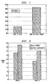
- the SLIC dominates the consumption of power in the cable modem. Further, the SLIC has never been viewed with the intention of reducing power, since they have traditionally been deployed in the CO and PBX environments. In these environments, the total power consumption is not dominated by the SLIC power. In the CM environment, however, the situation is very much different, as can be seen from Figure 2.
- Figure 2 illustrates that the SLIC is the single largest power consumer in a cable modem. The data presented herein above demonstrates that every 100mW of power saved translates into a saving of $2 in power cost.
- the present invention is directed to a low power SLIC that is particularly useful in bringing down costs associated with cable modems used to implement voice telephony services.
- the loop current has a DC as well as an AC component.
- the DC component (DC loop current) performs the function of delivering power to the telephone.
- the AC component is the speech signal.
- the power levels however, are vastly different: The DC power is a few hundred milliwatts, whereas the AC power is just a few milliwatts. It is the DC current feed then, which must be made efficient if one intends to make power feed efficient. At the same time, such an implementation must not disturb the performance of the AC voice band signals.
- One embodiment of the low power SLIC is implemented by having two current sources in parallel (one high efficiency, the other high fidelity) as illustrated by Figure 10.
- the DC current source has high efficiency and a high impedance in the voice band, while the AC current source synthesizes a 600 Ohm (typical) termination and does the high fidelity speech transmit and receiving (hybrid) functions.
- the DC current source then is optimized for efficiency while the AC current source is optimized for fidelity (voice band performance).
- the DC current source is implemented using switched-mode techniques.
- a subscriber line interface circuit is implemented using a switched-mode technique to provide a constant current source having high efficiency and that presents a high-impedance to the voice band signals.
- a subscriber line interface circuit is implemented using the "DUAL" of a voltage boost converter to provide a current boost converter constant current source having high efficiency and that present a high-impedance to the voice band signals.
- a subscriber line interface circuit is implemented using the "DUAL" of a switched-mode current-to-voltage trans-converter to provide a switched-mode voltage-to-current trans-converter constant current source having high efficiency and that presents a high-impedance to the voice band signals.
- the present invention is best understood by first providing a detailed discussion regarding DC power requirements of the telephone, efficiency of power feed from a subscriber line interface circuit, and the cost of wasted power associated with a particular subscriber loop. DC power requirements are considered first as set forth herein below.
- One of the primary functions of the SLIC is to feed DC power to the legacy telephone instruments.
- the early generation telephones used the loop current (typically 30mA or more) to power the carbon microphones.
- Present day speech circuit IC's require much less current and 20mA is considered more than sufficient for satisfactory operation of electronic phones.
- the DC V-I characteristics of phones are non-linear, but are expected to meet the characteristics of the EIA-470 standard, which is graphically shown in Figure 3 (only for currents below 40mA).
- Important issues related to this standard include: 1) performance of telephones is not guaranteed for currents below 20mA; 2) 400 Ohms is the maximum resistance that a phone can have in the range of 20mA to 30mA; and 3) 100 Ohms is the minimum resistance that a phone can have in the range of 20mA to 30mA. For purposes of loop current estimation and design of battery feed arrangements therefore, it is assumed that phones have a resistance of between 100 Ohms and 400 Ohms in the current range of 20mA to 30mA.
- the SLIC must now power up the phone to make it operate in this trapezoidal region 10. This can be done either with a voltage source or a current source. Either way, the V-I characteristics of the source must fall within the Bellcore limits shown in Figure 4.
- a current source is preferred because of its inherent short-circuit protection (the value of current being between 20mA and 30mA).
- a loop current of 20mA can be chosen. In this case, operation of the telephone is restricted to the vertical line at 20mA between the 100 Ohm and 400 Ohm resistance lines shown in Figure 3. Power consumption, among other things, can now be examined for this limited region of operation.
- FIG. 5 is a diagram illustrating off-hook constant current (CC) battery feed V-I characteristics associated with a subscriber line interface circuit subject to the conditions set forth herein before. This characteristic can be seen to have two distinct regions: the constant current (CC) region 12, and the voltage limiting (VL) region 14 (where the current drops). If the source has such a characteristic and the telephone has the characteristics shown in Figures 3 and 4, the phone by itself, when connected to such a source will get biased in the CC region. When a resistance (representing the line/loop resistance) is placed in series however, then the operating point could well be in the VL region 14, depending on the value of resistance.
- CC constant current
- VL voltage limiting
- the source is designed to operate in the CC region 12 for all values of loop length that is to be served.
- the maximum value of line resistance is about 16 Ohms (corresponding to the maximum loop length of 150 meters or 500 feet of AWG 22 wire). Adding to this the following:
- Minimization of power consumption can be illustrated by choosing the lowest possible value of current, i.e. 20mA.
- the efficiency ⁇ is very poor (56% at 400 Ohms, 44% at 300 Ohms, and just 31% at 200 Ohms).
- a low-power phone drops a small voltage and would present a lower resistance (say 300 Ohms or 200 Ohms) to the loop and will therefore consume less power.
- the phone consumes less power however, the power consumed by the SLIC remains the same. This is because the power not utilized by the phone is dissipated by the SLIC.
- a constant efficiency battery feed mechanism is required. This essentially means that is less power is to be delivered, then less power is actually consumed. This property is inherent in DC-DC converters or switched-mode power conversion.
- the benefits of such a power feed method can be examined by assuming that one can achieve, for example, a constant efficiency ⁇ of about 85%.
- Many DC-DC converters such as the model TPS5102 commercially available from Texas Instruments Incorporated of Dallas, Texas, can achieve however, efficiencies of more than 90%.
- the cost benefits are shown in Table 1 below that illustrates savings in power and cost by using a DC-DC converter to implement a constant efficiency batter feed mechanism.
- the loop current has a DC as well as an AC component.
- the DC component (DC loop current) performs the function of delivering power to the telephone.
- the AC component is the speech signal.
- the power levels however, are vastly different.
- the DC power is a few hundred milliwatts whereas the AC power is just a few milliwatts.
- the DC current source 22 preferably has high efficiency ( ⁇ ) between 85% and 90% as well as a high impedance in the voice band.
- the AC current source 24 synthesizes a 600 Ohm (typical) termination and accommodates the high fidelity speech transmit and receive functions (hybrid functions).
- the DC current source 22 is then optimized for efficiency while the AC current source 24 is optimized for fidelity (voice band performance).
- the DC current source 22 is most preferably implemented using switched-mode techniques.
- switched-mode converters disclosed in the literature are directed to voltage converters including 1) BUCK, illustrated in Figure 11, where the output voltage is always less than the input voltage; 2) BOOST, illustrated in Figure 12, where the output voltage is always greater than the input voltage; and 3) BUCK-BOOST, illustrated in Figure 13, where the output voltage can be less than or greater than the input voltage. None of these basic circuit topologies is suitable for implementing the desired constant DC current source for two reasons: First, they are constant voltage sources, and second (and more important), they all have a large capacitor at the output which will present a low impedance to voice band signals. Two switched-mode schemes including the dual of the voltage BOOST converter and the switched-mode voltage-to-current trans-converter, can however, be implemented to achieve the desired high efficiency while presenting a high impedance to the voice band signals.
- the dual of the voltage BOOST converter can be arrived at by converting one of the basic topologies depicted in Figures 11-13 into its respective "DUAL.”
- the "DUAL" of a circuit topology is like a "mirror image”, and is generally arrived at by: 1) replacing an inductor by a capacitor and vice-versa; and 2) replacing a current source by a voltage source and vice-versa; and 3) replacing a series element by the dual of the same element in shunt; and 4) replacing a shunt element by the dual of the same element in series; and 5) replacing a closed switch by an open switch and vice-versa.
- a first order analysis of converter 30 can be implemented, for example, by assuming 1) in the steady-state, there is no net build-up or no net loss of energy in the inductor 34 and the capacitor 36; and 2) the inductor 34 is large enough to have a very low ( ⁇ 1%) current ripple.
- the converter 30 has two distinct states including State-1 in which switch S1 is open and switch S2 is closed, and State-2 in which switch S1 is closed and switch S2 is open.
- the equivalent circuits corresponding to these two states are depicted in Figure 15.
- the analysis also assumes the duty cycle of the switching is ⁇ and the time period is T P . State-1 therefore, lasts for ⁇ T P seconds and State-2 lasts for (1- ⁇ ) T P seconds.
- a current boost circuit 40 is shown in Figure 17.
- one of the switches is usually a diode so as to simplify the control.
- Switch S2 then, is simply a fast recovery diode 42 that will turn off whenever switch S1 (transistor M1) 44 is turned on.
- the percentage of time for which the converter 40 is in State-1 is designated ⁇ , as stated herein before. This is the state in which S1 (transistor M1) 44 is off.
- the transistor M2 (46) is used to control transistor M1 (44).
- the driving signal for transistor M2 (46) should therefore have a duty cycle of (1- ⁇ ). It can be appreciated that the ⁇ has to be dynamically varied to keep the output current constant. This is easily achieved by using any industry standard PWM controller such as the TPS5102 or the TPS6734 commercially available from Texas Instruments Incorporated of Dallas, Texas.
- the current boost converter shown in Figure 17 discussed herein above is efficient provided there is a current source available.
- the primary power source however, is almost always a voltage source and not a current source.
- the input current source needs to be constructed from a voltage source. This is generally done with a linear element such as an op-amp or a transistor (operating in its linear region).
- the overall efficiency of a system using such a scheme will be the product of the efficiencies of the voltage-to-current converter (linear) and the current-to-current converter (switched-mode); and since the individual efficiencies are always less than 100%, the resultant efficiency will be less than the lower of the two efficiencies.
- One preferred embodiment for converting voltage to current employs a switched-mode voltage-to-current trans-converter. Operating principles of the switched-mode voltage-to-current trans-converter can be understood by first exploring the operating principles of a switched-mode current-to-voltage trans-converter.
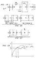
- FIG 19 illustrates a simplified switched-mode current-to-voltage transconverter 50.
- a capacitor C1 has been placed along with two switches, SW1 and SW2, to integrate the current and convert it into a fluctuating voltage that is later filtered by the filter of Figure 18 (formed by L1 and C2).
- the capacitor C1 is used to perform the actual current-to-voltage conversion while the capacitor C2 is part of the LC filter.
- the trans-converter 50 operates the switches, SW1 and SW2, alternately and in complimentary fashion (i.e. when one is on, the other is off). This can be represented as two states as shown in Figure 20.
- the change in voltage by an amount ⁇ V C also represents a change in energy ⁇ E C .
- V E C 1 2 C [( V 1 + ⁇ V C ) 2 - V 1 2 ]
- ⁇ E C represents both the increase in energy in State-2 as well as the decrease in energy in State-1.
- the resistor R L dissipates an energy E R ; and this energy has to come from the capacitor C1 since the source has been disconnected.
- the voltage ripple ⁇ V C can be estimated by considering the Thevenin equivalent circuit as shown by Figure 21, when the capacitor is being charged by the current source I S in State-2.
- An estimate of the ripple ⁇ V C , or the amount by which the capacitor C1 charges up in the interval ⁇ T P can be made by assuming that the capacitor C1 charges from ⁇ 1 at t 1 to ⁇ 2 at t 2 such as illustrated in Figure 22.
- FIG. 23 depicts implementation of a switched-mode current-to-voltage trans-converter.
- the switch S1 is implemented by the transistor M1 and the switch S2 is implemented by the diode D2.
- the diode D2 Whenever the transistor M1 is turned on, the diode D2 will be reverse biased and hence in its off state.
- trans-converter Since most power sources are voltage sources, and because what is needed on the subscriber loop is a constant current source, it is more useful to have a voltage-to-current trans-converter.
- Such a trans-converter can be a dual of the current-to-voltage trans-converter that was described herein before with reference to Figures 18-23. It can easily be ascertained that because of the "duality" principle, all equations and waveforms are similar to that of the current-to-voltage trans-converter.
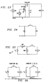
- the trans-converter 60 shown in Figure 25 operates the switches SW1 and SW2 alternately and in complimentary fashion (when one is on, the other is off). This can be represented as two states as shown in Figure 26. There is a build-up of current in the inductor L1 in State-2 and a decrease in the inductor L1 current in State-1.
- the duty cycle can be adjusted (with an error amplifier and a PWM controller well known in the art) so that the current through the load R L remains constant regardless of the value of R L .
- the function of the LC filter shown in Figure 24 is merely to filter out the current ripple of the inductor; and it does not play any role in the current-to-voltage conversion. This is ensured by making the cut-off frequency of the LC filter much smaller than the switching frequency.
- the LC filter is therefore not shown in Figure 26 since it need not be considered in the analysis.
- the inductor supplies the load current I O in State-2. This causes the current through the inductor to droop by an amount ⁇ I L .
- the inductor current builds up by the same amount (assuming a steady-state condition where there is neither a net increase nor a net decrease of energy). Since the current through the inductor represents a stored energy, the change in current through the inductor represents a stored energy.
- the ⁇ E L term represents both and increase in energy in State-1 as well as a decrease in energy in State-2. In State-2, for a duration (1- ⁇ ) T P , the resistor R L dissipate an energy E R that must be provided by the inductor since the source has been disconnected.
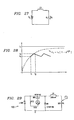
- An estimate of the current ripple ⁇ I L (amount by which the inductor charges up in the interval ⁇ T P ) can be made by assuming that the inductor charges from current I 1 at time t 1 to current I 2 at time t 2 , as shown in Figure 28 that depicts the inductor current waveform caused by charging of the inductor by the voltage source in State-1.
- the present invention presents a significant advancement in the art of switched-mode current feed techniques for subscriber loops employed in telephony applications. Further, this invention has been described in considerable detail in order to provide those skilled in the data communication art with the information needed to apply the novel principles and to construct and use such specialized components as are required. In view of the foregoing descriptions, it should further be apparent that the present invention represents a significant departure from the prior art in construction and operation. However, while particular embodiments of the present invention have been described herein in detail, it is to be understood that various alterations, modifications and substitutions can be made therein without departing in any way from the spirit and scope of the present invention, as defined in the claims which follow.
Landscapes
- Engineering & Computer Science (AREA)
- Power Engineering (AREA)
- Signal Processing (AREA)
- Dc-Dc Converters (AREA)
- Interface Circuits In Exchanges (AREA)
- Telephone Function (AREA)
- Devices For Supply Of Signal Current (AREA)
Abstract
Description
| Savings in power and cost by using a DC-DC converter | |||||
| Cost of wasted power | |||||
| RL | Ploop | Pcon | Pcon(DC-DC) | Psaved | $ Saved |
| 200 | 320 | 1232 | 376 | 856 | 17.11 |
| 225 | 360 | 1232 | 424 | 808 | 16.17 |
| 250 | 400 | 1232 | 471 | 761 | 15.23 |
| 275 | 440 | 1232 | 518 | 714 | 14.29 |
| 300 | 480 | 1232 | 565 | 667 | 13.35 |
| 325 | 520 | 1232 | 612 | 620 | 12.40 |
| 350 | 560 | 1232 | 659 | 573 | 11.46 |
| 375 | 600 | 1232 | 706 | 526 | 10.52 |
| 400 | 640 | 1232 | 753 | 479 | 9.58 |
| 425 | 680 | 1232 | 800 | 432 | 8.64 |
| 450 | 720 | 1232 | 847 | 385 | 7.70 |
| 475 | 760 | 1232 | 894 | 338 | 6.76 |
| 500 | 800 | 1232 | 941 | 291 | 5.82 |
| 525 | 840 | 1232 | 988 | 244 | 4.88 |
| 550 | 880 | 1232 | 1035 | 197 | 3.93 |
I OUT therefore is greater than I IN , which proves the BOOST operation of the current source. Moreover, the magnitude of Δ V C 1 is equal to the magnitude of ΔV C 2, which means
I=C dV / dt or V C (t)= 1 t / C 0 i(t*)dt* is used to convert current into voltage by accumulating
(or integrating) the current flowing into a capacitor. The load needs a constant voltage, and hence, one can insert an LC filter such as shown in Figure 18, before the load to smoothen out any voltage fluctuations. A fluctuating voltage applied across points "A" and "B" in Figure 18 will therefore appear filtered across R LOAD. If a current source is periodically switched onto a capacitor to create a fluctuating voltage, it can then be filtered using an LC filter such as depicted in Figure 18. One such filtered current source is shown in Figure 19 that illustrates a simplified switched-mode current-to-voltage transconverter 50. Here, a capacitor C1 has been placed along with two switches, SW1 and SW2, to integrate the current and convert it into a fluctuating voltage that is later filtered by the filter of Figure 18 (formed by L1 and C2). It can be appreciated that the capacitor C1 is used to perform the actual current-to-voltage conversion while the capacitor C2 is part of the LC filter. The trans-converter 50 operates the switches, SW1 and SW2, alternately and in complimentary fashion (i.e. when one is on, the other is off). This can be represented as two states as shown in Figure 20. There is a build-up of voltage on the capacitor C1 in State-2, and a decrease in voltage on the capacitor C1 in State-1. The duty cycle can be so adjusted (i.e. using an error amplifier and a PWM controller familiar to those skilled in the art) such that the voltage on the load remains constant regardless of the value of R LOAD.



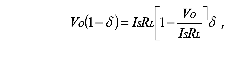
| δ | V0 using Eq (18) | V0 from simulation | Error |
| 0.2 | 1.87 | 1.78 | -5.06% |
| 0.5 | 4.675 | 4.64 | -0.75% |
| 0.7 | 6.55 | 6.57 | 0.30% |
| 0.8 | 7.48 | 7.53 | 0.66% |
| 0.9 | 8.42 | 8.48 | 0.71% |
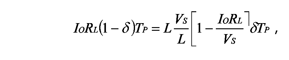
I L = I f [1- e -t /τ], where I f= V S / R L . An estimate of the current ripple Δ I L (amount by which the inductor charges up in the interval δT P ) can be made by assuming that the inductor charges from current I 1 at time t 1 to current I 2 at time t 2, as shown in Figure 28 that depicts the inductor current waveform caused by charging of the inductor by the voltage source in State-1. Using the foregoing assumption, the current ripple ΔI L can now be estimated by recognizing that



| δ | IO (calculated) | IO (simulated) | Error |
| 0.1 | 10 | 11.64 | 16.40% |
| 0.2 | 20 | 20.51 | 2.55% |
| 0.3 | 30 | 30.06 | 0.20% |
| 0.4 | 40 | 39.85 | -0.37% |
| 0.5 | 50 | 49.68 | -0.64% |
| 0.6 | 60 | 59.73 | -0.45% |
| 0.8 | 80 | 79.99 | -0.01% |
| 0.9 | 90 | 90.01 | -0.01% |
Claims (25)
- A subscriber loop interface circuit comprising:an AC current source configured to synthesize a desired impedance termination and further to implement high fidelity speech transmit and receiving functions; anda constant DC current source in parallel with the AC current source and configured to have an efficiency of at least 80% and further to present a high impedance to voice band signals.
- The subscriber loop interface circuit according to claim 1 wherein the DC current source comprises a switched-mode current boost converter.
- The subscriber loop interface circuit according to claim 2 wherein the switched-mode current boost converter comprises a first semiconductor switch and a second semiconductor switch, wherein the first and second semiconductor switches are configured such that when the first semiconductor switch is open, the second semiconductor switch is closed to implement a first state, and further such that when the first semiconductor switch is closed, the second semiconductor switch is open to implement a second state.
- The subscriber loop interface circuit according to claim 3 wherein the switched-mode current boost converter further comprises a capacitor configured to be charged by a current source when the first and second semiconductor switches are in the first state, and further configured to be discharging when the first and second semiconductor switches are in the second state.
- The subscriber loop interface circuit according to claim 4 wherein the switched-mode current boost converter further comprises a series inductor at its output, wherein the inductor is operational to achieve the high impedance in a subscriber line voice band, and further wherein the inductor has an inductance that is sufficient to limit converter output current ripple to less than about one percent.
- The subscriber loop interface circuit according to claim 5 wherein the first semiconductor switch comprises a CMOS transistor that is operational in response to a dynamically time varied input signal to cause the switched-mode current boost converter to switch between its first and second states to maintain a constant output current.
- The subscriber loop interface circuit according to claim 6 wherein the second semiconductor switch comprises a fast response diode that is operational to switch alternately and in complimentary fashion with the CMOS transistor in response to the dynamically time varied input signal.
- The subscriber loop interface circuit according to claim 1 wherein the DC current source comprises a switched-mode voltage-to-current trans-converter.
- The subscriber loop interface circuit according to claim 8 wherein the switched-mode voltage-to-current trans-converter comprises a first semiconductor switch and a second semiconductor switch, wherein the first and second semiconductor switches are configured such that when the first semiconductor switch is open, the second semiconductor switch is closed to implement a first state, and further such that when the first semiconductor switch is closed, the second semiconductor switch is open to implement a second state.
- The subscriber loop interface circuit according to claim 9 wherein the switched-mode voltage-to-current trans-converter converter further comprises a series inductor at its output, wherein the inductor is operational to achieve the high impedance in a subscriber line voice band, and further wherein the inductor has an inductance that is sufficient to limit trans-converter output current ripple to no more than about one percent.
- The subscriber loop interface circuit according to claim 10 wherein the first semiconductor switch comprises a CMOS transistor that is operational in response to a dynamically time varied input signal to cause the switched-mode voltage-to-current trans-converter to switch between its first and second states to maintain a constant output current.
- The subscriber loop interface circuit according to claim 11 wherein the second semiconductor switch comprises a fast response diode that is operational to switch alternately and in complimentary fashion with the CMOS transistor in response to the dynamically time varied input signal.
- A subscriber loop interface circuit comprising:a switched-mode current boost converter configured to provide a constant DC current feed to a subscriber line, wherein the current boost converter includes:at least one capacitor;at least one output series inductor;a first switch; anda second switch, wherein the first and second switches are responsive to a dynamically time varied input signal to switch alternately and in complementary fashion to implement a first state and a second state such that the at least one capacitor is caused to be charged by a current source while in the first state and to be discharging via the at least one output series inductor while in the second state to generate the constant DC current feed.
- The subscriber loop interface circuit according to claim 13 further comprising an AC current source configured to synthesize a subscriber line termination impedance and to implement subscriber line high fidelity speech transmit and receiving functions.
- The subscriber loop interface circuit according to claim 13 wherein the first switch comprises a CMOS transistor that is operational in response to the dynamically time varied input signal to cause the switched-mode current boost converter to switch between its first and second states to maintain a constant DC output current.
- The subscriber loop interface circuit according to claim 15 wherein the second switch comprises a fast response diode that is operational to switch alternately and in complimentary fashion with the CMOS transistor in response to the dynamically time varied input signal.
- The subscriber loop interface circuit according to claim 13 wherein the dynamically time varied input signal is generated via a pulse width modulated controller.
- A subscriber loop interface circuit comprising:a switched-mode voltage-to-current trans-converter configured to provide a constant DC current feed to a subscriber line, wherein the voltge-to-current trans-converter includes:at least one output series inductor;a first switch; anda second switch, wherein the first and second switches are responsive to a dynamically time varied input signal to switch alternately and in complementary fashion to implement a first state and a second state such that the at least one output series inductor is caused to be charged by a voltage source while in the first state and to be discharging via the subscriber line while in the second state to generate the constant DC current feed.
- The subscriber loop interface circuit according to claim 18 further comprising an AC current source configured to synthesize a subscriber line termination impedance and to implement subscriber line high fidelity speech transmit and receiving functions.
- The subscriber loop interface circuit according to claim 18 wherein the first switch comprises a CMOS transistor that is operational in response to the dynamically time varied input signal to cause the switched-mode voltage-to-current trans-converter to switch between its first and second states to maintain a constant DC output current.
- The subscriber loop interface circuit according to claim 20 wherein the second switch comprises a fast response diode that is operational to switch alternately and in complimentary fashion with the CMOS transistor in response to the dynamically time varied input signal.
- The subscriber loop interface circuit according to claim 18 wherein the dynamically time varied input signal is generated via a pulse width modulated controller.
- A method of generating a subscriber line constant DC current feed comprising the steps of:(a) providing a switched-mode current boost converter having a charging/discharging capacitor and further having a series output inductor coupled to the subscriber line;(b) charging the capacitor via a current source for a first time period in response to a dynamically time variable input signal; and(c) discharging the capacitor via the series output inductor for a second time period in response to the dynamically time variable input signal such that there is neither a net increase nor a net decrease of energy in the inductor and the capacitor, and further to generate a constant DC output current to the subscriber line, wherein the DC output current has a magnitude that is greater than the source current that is operative to charge the capacitor.
- A method of generating a subscriber line constant DC current feed comprising the steps of:(a) providing a switched-mode voltage-to- current trans-converter having a series output inductor coupled to the subscriber line;(b) charging the inductor via a voltage source for a first time period in response to a dynamically time variable input signal; and(c) discharging the inductor via the subscriber line for a second time period in response to the dynamically time variable input signal such that there is neither a net increase nor a net decrease of energy in the inductor, and further to generate a constant DC output current to the subscriber line such that the DC output current has a magnitude that remains constant with changing subscriber line impedance.
- A subscriber loop interface circuit comprising:means for synthesizing a subscriber line termination impedance and further for implementing high fidelity speech transmit and receiving functions; andmeans for generating a subscriber line constant DC current and for presenting a high impedance to subscriber line voice band signals, wherein the generating means has an efficiency of at least 80%.
Applications Claiming Priority (2)
| Application Number | Priority Date | Filing Date | Title |
|---|---|---|---|
| US25477900P | 2000-12-11 | 2000-12-11 | |
| US254779 | 2000-12-11 |
Publications (3)
| Publication Number | Publication Date |
|---|---|
| EP1213907A2 true EP1213907A2 (en) | 2002-06-12 |
| EP1213907A3 EP1213907A3 (en) | 2004-12-29 |
| EP1213907B1 EP1213907B1 (en) | 2011-05-18 |
Family
ID=22965557
Family Applications (1)
| Application Number | Title | Priority Date | Filing Date |
|---|---|---|---|
| EP01000734A Expired - Lifetime EP1213907B1 (en) | 2000-12-11 | 2001-12-10 | switched mode current feed methods for telephony subcriber loops |
Country Status (4)
| Country | Link |
|---|---|
| US (1) | US20020110236A1 (en) |
| EP (1) | EP1213907B1 (en) |
| JP (1) | JP4088067B2 (en) |
| AT (1) | ATE510404T1 (en) |
Families Citing this family (7)
| Publication number | Priority date | Publication date | Assignee | Title |
|---|---|---|---|---|
| US6480510B1 (en) | 1998-07-28 | 2002-11-12 | Serconet Ltd. | Local area network of serial intelligent cells |
| US6956826B1 (en) | 1999-07-07 | 2005-10-18 | Serconet Ltd. | Local area network for distributing data communication, sensing and control signals |
| US6690677B1 (en) * | 1999-07-20 | 2004-02-10 | Serconet Ltd. | Network for telephony and data communication |
| US6549616B1 (en) | 2000-03-20 | 2003-04-15 | Serconet Ltd. | Telephone outlet for implementing a local area network over telephone lines and a local area network using such outlets |
| IL154234A (en) | 2003-01-30 | 2010-12-30 | Mosaid Technologies Inc | Method and system for providing dc power on local telephone lines |
| IL159838A0 (en) | 2004-01-13 | 2004-06-20 | Yehuda Binder | Information device |
| JP2011171834A (en) * | 2010-02-16 | 2011-09-01 | Panasonic Electric Works Co Ltd | Communication system and electronic choke circuit |
Family Cites Families (7)
| Publication number | Priority date | Publication date | Assignee | Title |
|---|---|---|---|---|
| GB2071461B (en) * | 1980-02-14 | 1984-01-25 | Standard Telephones Cables Ltd | Telephone line feed |
| DE3171608D1 (en) * | 1981-10-28 | 1985-09-05 | Ibm | Line circuit containing impedance adaptation means |
| US4674119A (en) * | 1984-04-10 | 1987-06-16 | Itt Corporation | Wide-band high voltage amplifier for telephone exchange subscriber line interface utilizing low voltage control circuitry |
| DE69120135T2 (en) * | 1990-04-04 | 1997-01-23 | Seiscor Tech Inc | Interface circuit for subscriber line that supplies regulated electricity |
| JPH0851651A (en) * | 1994-06-24 | 1996-02-20 | Harris Corp | Subscriber line interface circuit, impedance matching method, and hybrid echo cancellation method |
| US6728370B1 (en) * | 1999-03-15 | 2004-04-27 | Legerity, Inc. | Method and apparatus for impedance matching |
| US6668060B1 (en) * | 1999-10-26 | 2003-12-23 | Adtran, Inc. | Tracking switchmode power converter for telephony interface circuit |
-
2001
- 2001-12-10 US US10/016,778 patent/US20020110236A1/en not_active Abandoned
- 2001-12-10 JP JP2001375882A patent/JP4088067B2/en not_active Expired - Fee Related
- 2001-12-10 EP EP01000734A patent/EP1213907B1/en not_active Expired - Lifetime
- 2001-12-10 AT AT01000734T patent/ATE510404T1/en not_active IP Right Cessation
Also Published As
| Publication number | Publication date |
|---|---|
| ATE510404T1 (en) | 2011-06-15 |
| JP4088067B2 (en) | 2008-05-21 |
| JP2002218512A (en) | 2002-08-02 |
| EP1213907A3 (en) | 2004-12-29 |
| US20020110236A1 (en) | 2002-08-15 |
| EP1213907B1 (en) | 2011-05-18 |
Similar Documents
| Publication | Publication Date | Title |
|---|---|---|
| US5103387A (en) | High voltage converter | |
| US6049471A (en) | Controller for pulse width modulation circuit using AC sine wave from DC input signal | |
| US6917681B2 (en) | Peak power management and active decoupling arrangement for span-powered remote terminal access platforms | |
| EP1264382A2 (en) | Ultra-low power switching regulator method and apparatus with adaptively adjustable switching frequency and peak current trip point | |
| GB2029989A (en) | Automatic control converters | |
| EP1331720B1 (en) | Programmable dual mode hysteretic power output controller | |
| EP1213907B1 (en) | switched mode current feed methods for telephony subcriber loops | |
| CN105612683A (en) | Voltage regulator with charge pump for generating second voltage source | |
| US20090243578A1 (en) | Power Supply with Digital Control Loop | |
| US6310953B1 (en) | Subscriber circuit | |
| CA1159975A (en) | Communication system signaling circuit | |
| US20070076455A1 (en) | Voltage regulator with common s-phase signals and phase lock loops | |
| CN1262551A (en) | Dual-output power supply with high voltage stability and high precision | |
| US20090243572A1 (en) | Power Supply with Digital Control Loop | |
| US20060269052A1 (en) | Switched mode current feed methods for telephony subscriber loops | |
| US6307357B1 (en) | Direct current step-up circuit for use with battery powered equipment | |
| US7076055B2 (en) | Tracking switchmode power converter for telephony interface circuit | |
| US20090245504A1 (en) | Power Supply with Digital Control Loop | |
| EP2802135B1 (en) | DC/DC Converter and Subscriber Line Interface Circuit | |
| US11881775B2 (en) | Systems and methods to remove input voltage dependency in a power converter | |
| US9014367B2 (en) | DC/DC converter for a subscriber line interface circuit, system, method and apparatus | |
| US20090243701A1 (en) | Power Supply with Digital Control Loop | |
| JP3078292B2 (en) | Call current supply method | |
| JP5288481B2 (en) | Subscriber line interface device and power supply method thereof | |
| JP4160706B2 (en) | Subscriber circuit power supply system |
Legal Events
| Date | Code | Title | Description |
|---|---|---|---|
| PUAI | Public reference made under article 153(3) epc to a published international application that has entered the european phase |
Free format text: ORIGINAL CODE: 0009012 |
|
| AK | Designated contracting states |
Kind code of ref document: A2 Designated state(s): AT BE CH CY DE DK ES FI FR GB GR IE IT LI LU MC NL PT SE TR |
|
| AX | Request for extension of the european patent |
Free format text: AL;LT;LV;MK;RO;SI |
|
| PUAL | Search report despatched |
Free format text: ORIGINAL CODE: 0009013 |
|
| AK | Designated contracting states |
Kind code of ref document: A3 Designated state(s): AT BE CH CY DE DK ES FI FR GB GR IE IT LI LU MC NL PT SE TR |
|
| AX | Request for extension of the european patent |
Extension state: AL LT LV MK RO SI |
|
| 17P | Request for examination filed |
Effective date: 20050629 |
|
| AKX | Designation fees paid |
Designated state(s): AT BE CH CY DE DK ES FI FR GB GR IE IT LI LU MC NL PT SE TR |
|
| 17Q | First examination report despatched |
Effective date: 20061019 |
|
| GRAP | Despatch of communication of intention to grant a patent |
Free format text: ORIGINAL CODE: EPIDOSNIGR1 |
|
| GRAS | Grant fee paid |
Free format text: ORIGINAL CODE: EPIDOSNIGR3 |
|
| GRAA | (expected) grant |
Free format text: ORIGINAL CODE: 0009210 |
|
| AK | Designated contracting states |
Kind code of ref document: B1 Designated state(s): AT BE CH CY DE DK ES FI FR GB GR IE IT LI LU MC NL PT SE TR |
|
| REG | Reference to a national code |
Ref country code: GB Ref legal event code: FG4D |
|
| REG | Reference to a national code |
Ref country code: CH Ref legal event code: EP |
|
| REG | Reference to a national code |
Ref country code: IE Ref legal event code: FG4D |
|
| REG | Reference to a national code |
Ref country code: DE Ref legal event code: R096 Ref document number: 60144645 Country of ref document: DE Effective date: 20110630 |
|
| REG | Reference to a national code |
Ref country code: NL Ref legal event code: T3 |
|
| PG25 | Lapsed in a contracting state [announced via postgrant information from national office to epo] |
Ref country code: SE Free format text: LAPSE BECAUSE OF FAILURE TO SUBMIT A TRANSLATION OF THE DESCRIPTION OR TO PAY THE FEE WITHIN THE PRESCRIBED TIME-LIMIT Effective date: 20110518 Ref country code: PT Free format text: LAPSE BECAUSE OF FAILURE TO SUBMIT A TRANSLATION OF THE DESCRIPTION OR TO PAY THE FEE WITHIN THE PRESCRIBED TIME-LIMIT Effective date: 20110919 |
|
| PG25 | Lapsed in a contracting state [announced via postgrant information from national office to epo] |
Ref country code: FI Free format text: LAPSE BECAUSE OF FAILURE TO SUBMIT A TRANSLATION OF THE DESCRIPTION OR TO PAY THE FEE WITHIN THE PRESCRIBED TIME-LIMIT Effective date: 20110518 Ref country code: ES Free format text: LAPSE BECAUSE OF FAILURE TO SUBMIT A TRANSLATION OF THE DESCRIPTION OR TO PAY THE FEE WITHIN THE PRESCRIBED TIME-LIMIT Effective date: 20110829 Ref country code: BE Free format text: LAPSE BECAUSE OF FAILURE TO SUBMIT A TRANSLATION OF THE DESCRIPTION OR TO PAY THE FEE WITHIN THE PRESCRIBED TIME-LIMIT Effective date: 20110518 Ref country code: CY Free format text: LAPSE BECAUSE OF FAILURE TO SUBMIT A TRANSLATION OF THE DESCRIPTION OR TO PAY THE FEE WITHIN THE PRESCRIBED TIME-LIMIT Effective date: 20110518 Ref country code: AT Free format text: LAPSE BECAUSE OF FAILURE TO SUBMIT A TRANSLATION OF THE DESCRIPTION OR TO PAY THE FEE WITHIN THE PRESCRIBED TIME-LIMIT Effective date: 20110518 Ref country code: GR Free format text: LAPSE BECAUSE OF FAILURE TO SUBMIT A TRANSLATION OF THE DESCRIPTION OR TO PAY THE FEE WITHIN THE PRESCRIBED TIME-LIMIT Effective date: 20110819 |
|
| PG25 | Lapsed in a contracting state [announced via postgrant information from national office to epo] |
Ref country code: DK Free format text: LAPSE BECAUSE OF FAILURE TO SUBMIT A TRANSLATION OF THE DESCRIPTION OR TO PAY THE FEE WITHIN THE PRESCRIBED TIME-LIMIT Effective date: 20110518 |
|
| PLBE | No opposition filed within time limit |
Free format text: ORIGINAL CODE: 0009261 |
|
| STAA | Information on the status of an ep patent application or granted ep patent |
Free format text: STATUS: NO OPPOSITION FILED WITHIN TIME LIMIT |
|
| 26N | No opposition filed |
Effective date: 20120221 |
|
| PG25 | Lapsed in a contracting state [announced via postgrant information from national office to epo] |
Ref country code: IT Free format text: LAPSE BECAUSE OF FAILURE TO SUBMIT A TRANSLATION OF THE DESCRIPTION OR TO PAY THE FEE WITHIN THE PRESCRIBED TIME-LIMIT Effective date: 20110518 |
|
| REG | Reference to a national code |
Ref country code: DE Ref legal event code: R097 Ref document number: 60144645 Country of ref document: DE Effective date: 20120221 |
|
| PG25 | Lapsed in a contracting state [announced via postgrant information from national office to epo] |
Ref country code: MC Free format text: LAPSE BECAUSE OF NON-PAYMENT OF DUE FEES Effective date: 20111231 |
|
| REG | Reference to a national code |
Ref country code: CH Ref legal event code: PL |
|
| PG25 | Lapsed in a contracting state [announced via postgrant information from national office to epo] |
Ref country code: CH Free format text: LAPSE BECAUSE OF NON-PAYMENT OF DUE FEES Effective date: 20111231 Ref country code: LI Free format text: LAPSE BECAUSE OF NON-PAYMENT OF DUE FEES Effective date: 20111231 |
|
| PG25 | Lapsed in a contracting state [announced via postgrant information from national office to epo] |
Ref country code: LU Free format text: LAPSE BECAUSE OF NON-PAYMENT OF DUE FEES Effective date: 20111210 |
|
| PG25 | Lapsed in a contracting state [announced via postgrant information from national office to epo] |
Ref country code: TR Free format text: LAPSE BECAUSE OF FAILURE TO SUBMIT A TRANSLATION OF THE DESCRIPTION OR TO PAY THE FEE WITHIN THE PRESCRIBED TIME-LIMIT Effective date: 20110518 |
|
| REG | Reference to a national code |
Ref country code: FR Ref legal event code: PLFP Year of fee payment: 15 |
|
| REG | Reference to a national code |
Ref country code: FR Ref legal event code: PLFP Year of fee payment: 16 |
|
| PGFP | Annual fee paid to national office [announced via postgrant information from national office to epo] |
Ref country code: GB Payment date: 20161125 Year of fee payment: 16 Ref country code: NL Payment date: 20161207 Year of fee payment: 16 Ref country code: IE Payment date: 20161125 Year of fee payment: 16 Ref country code: FR Payment date: 20161117 Year of fee payment: 16 |
|
| PGFP | Annual fee paid to national office [announced via postgrant information from national office to epo] |
Ref country code: DE Payment date: 20161220 Year of fee payment: 16 |
|
| REG | Reference to a national code |
Ref country code: DE Ref legal event code: R119 Ref document number: 60144645 Country of ref document: DE |
|
| REG | Reference to a national code |
Ref country code: NL Ref legal event code: MM Effective date: 20180101 |
|
| GBPC | Gb: european patent ceased through non-payment of renewal fee |
Effective date: 20171210 |
|
| REG | Reference to a national code |
Ref country code: IE Ref legal event code: MM4A |
|
| PG25 | Lapsed in a contracting state [announced via postgrant information from national office to epo] |
Ref country code: NL Free format text: LAPSE BECAUSE OF NON-PAYMENT OF DUE FEES Effective date: 20180101 |
|
| REG | Reference to a national code |
Ref country code: FR Ref legal event code: ST Effective date: 20180831 |
|
| PG25 | Lapsed in a contracting state [announced via postgrant information from national office to epo] |
Ref country code: DE Free format text: LAPSE BECAUSE OF NON-PAYMENT OF DUE FEES Effective date: 20180703 Ref country code: IE Free format text: LAPSE BECAUSE OF NON-PAYMENT OF DUE FEES Effective date: 20171210 Ref country code: FR Free format text: LAPSE BECAUSE OF NON-PAYMENT OF DUE FEES Effective date: 20180102 |
|
| PG25 | Lapsed in a contracting state [announced via postgrant information from national office to epo] |
Ref country code: GB Free format text: LAPSE BECAUSE OF NON-PAYMENT OF DUE FEES Effective date: 20171210 |