EP1213758A1 - A method of forming interconnections in semiconductor devices - Google Patents
A method of forming interconnections in semiconductor devices Download PDFInfo
- Publication number
- EP1213758A1 EP1213758A1 EP00830810A EP00830810A EP1213758A1 EP 1213758 A1 EP1213758 A1 EP 1213758A1 EP 00830810 A EP00830810 A EP 00830810A EP 00830810 A EP00830810 A EP 00830810A EP 1213758 A1 EP1213758 A1 EP 1213758A1
- Authority
- EP
- European Patent Office
- Prior art keywords
- layer
- conductive material
- openings
- connection elements
- removable
- Prior art date
- Legal status (The legal status is an assumption and is not a legal conclusion. Google has not performed a legal analysis and makes no representation as to the accuracy of the status listed.)
- Granted
Links
Images


Classifications
-
- H—ELECTRICITY
- H10—SEMICONDUCTOR DEVICES; ELECTRIC SOLID-STATE DEVICES NOT OTHERWISE PROVIDED FOR
- H10W—GENERIC PACKAGES, INTERCONNECTIONS, CONNECTORS OR OTHER CONSTRUCTIONAL DETAILS OF DEVICES COVERED BY CLASS H10
- H10W20/00—Interconnections in chips, wafers or substrates
- H10W20/01—Manufacture or treatment
- H10W20/031—Manufacture or treatment of conductive parts of the interconnections
- H10W20/063—Manufacture or treatment of conductive parts of the interconnections by forming conductive members before forming protective insulating material
Definitions
- the present invention relates to electronic semiconductor devices having electrical interconnection structures on a substrate and, more particularly, to a method of forming these interconnection structures.
- the most usual method of forming interconnections up to now provides for the formation of a dielectric layer having openings for contact with an underlying layer, the deposition of a layer of metal, typically aluminium, on the dielectric layer, and selective etching of the metal layer by photolithographic techniques to form the necessary interconnection elements.
- This method has various disadvantages, that is: a poor ability to cover stepped structures so that the conductive tracks tend to become thinner on the walls of the openings, poor dimensional control when interconnection elements are defined by wet chemical etching, and other problems with dry etching when the nature of the metal permits it (aluminium can easily be etched dry but copper or gold cannot).
- planarizing techniques for example, chemical-mechanical polishing (or CMP), which further complicate the production process and may introduce defects and contamination.
- the main object of the present invention is to provide a method of forming semiconductor devices with high-conductivity interconnections and with insulators having low dielectric constants.
- a substrate 10 of semiconductor material for example, monocrystalline silicon, is treated by the usual processes for the manufacture of integrated circuits to produce a plurality of components, some of which are already interconnected and some of which are to be connected to one another or to external terminals.
- Figure 1 shows two diffused regions 12 having respective areas to be contacted on the substrate surface.
- a layer of insulating material for example, silicon dioxide, is formed on the substrate 10. Openings are formed in the insulating layer, for example, by reactive ion etching (or RIE) through a photoresist mask (not shown).
- a metal for example, tungsten, is applied to the insulating layer and in the openings, for example, by chemical vapour deposition (or CVD).
- the metal is then removed from the surface of the insulating layer, for example, by a chemical-mechanical polishing (CMP) process, to produce an insulating layer 11, for example, 300-2000 nm thick, with a flat surface and with openings 13 filled by conductive connection elements or plugs 14.
- CMP chemical-mechanical polishing
- a barrier layer (not shown) composed of titanium and of titanium nitride, 50-100 nm thick, is formed on the walls and on the base of the openings 13.
- a thin layer 15 (for example 100 nm) of a conductive material, which will be called the barrier layer and the functions of which will be explained below, is then formed ( Figure 2).
- the layer 15 is titanium nitride (TiN) produced by chemical vapour deposition (CVD).
- a layer 16 of a conductive material the main characteristic of which is that it can be removed completely in a final step of the method is deposited on the barrier layer 15.
- This material preferably has the following properties: it has a conductivity of 50 S/cm or more, it can be deposited in a uniform film, it has good adhesion to the materials with which it is in contact in the method, and it can be removed completely by chemical means or by plasma etching.
- a material with these properties is polyaniline (C 6 H 5 NH 3 ) treated so as to be conductive.
- Polyaniline is a polymer which can easily be applied in a uniform layer by the usual method for the deposition of a material in the liquid state on a spinning substrate and subsequent drying.
- Another material usable for the purpose is graphite, preferably applied by cathodic sputtering.
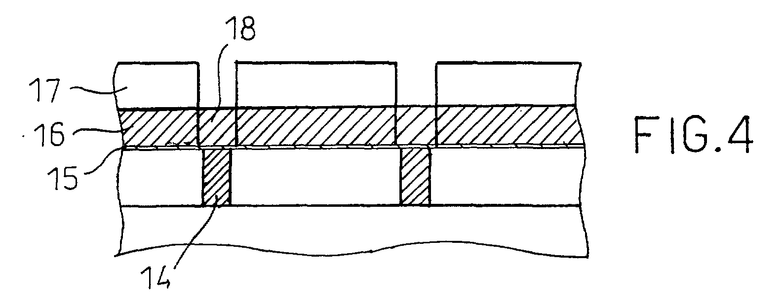
- the thickness of the layer 16 is selected so as to be equal to that of the interconnection elements (18, Figure 4) which are to be formed by the subsequent steps.
- a photoresist layer 17 is deposited and is treated to form a mask which leaves the areas above the tungsten plugs 14 exposed; the exposed conductive layer 16 is removed, for example, by anisotropic plasma etching, if it is polyaniline, to form openings 9 which expose the barrier layer 15, as shown in Figure 3.
- interconnection elements 18 are formed by the electrochemical deposition of a metal having good conductivity, for example, copper.
- a metal having good conductivity for example, copper.
- the process is made possible by the fact that the conductive layers 15 and 16 allow current to flow from the edges of the substrate to the tops of the tungsten plugs 14.
- the copper interconnection elements 18 are shown with exactly the same thickness as the conductive layer 16. This alignment is advisable, but some positive or negative nonalignment can be tolerated; the duration of the electrochemical deposition process is therefore not critical.
- the layer 15 also has the function of preventing copper atoms from diffusing into the insulating layer 11, which is preferably silicon dioxide, or into the insulating material which will be formed during the subsequent steps of the method.
- openings having a high height/width ratio it may be advantageous to limit the growth of the metal to growth purely from the bases of the openings 9. This can be achieved by rendering the layer 16 non-conductive in the vicinity of the walls of the openings 9.
- an alkaline liquid for example, ammonia in aqueous solution (NH 4 OH).
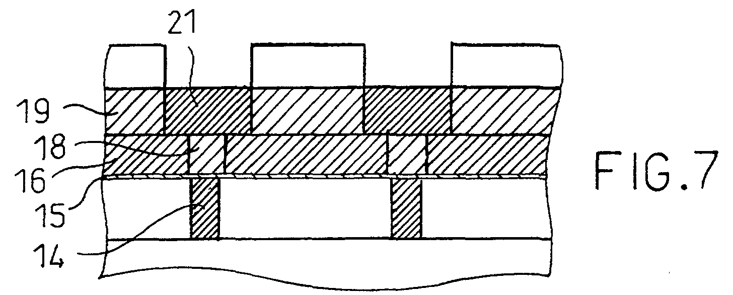
- the method continues with the deposition of a second layer 19 (Figure 5) of removable conductive material, for example, treated polyaniline again, by the opening, in the second layer 19, ( Figure 6) of through channels 20 above the elements 18 to be connected to one another, and/or of vias for connection to external terminals, and by the filling of these channels and/or vias with a second electrochemical deposition of metal, for example, copper again ( Figure 7), to form interconnection tracks and/or vias 21.
- a second layer 19 Figure 5
- removable conductive material for example, treated polyaniline again
- the conductive material of the layers 15, 16 and 19 is removed so as to insulate all of the interconnection tracks and vias from one another as shown in Figure 8.
- the layers 16 and 19 can be removed by chemical means with the usual photoresist-removal baths, or by isotropic etching in oxygen plasma.
- the layer 15 (TiN) can be removed by isotropic etching in plasma, which may possibly be the same as is used to remove the layers 16 and 19.
- the portions of the layer 15 which are disposed between the connection elements 18 and the tungsten plugs 14 are not removed by the isotropic etching, except to a negligible extent at the edges.
- a layer 22 of a dielectric material with a low dielectric constant is then formed and fills all of the spaces between the insulating layer 11 and the interconnection elements 18, 21.
- an aerogel is used, that is, a porous siliceous material the pores of which have diameters of a few nanometres and which has a very low dielectric constant, typically less than half of that of dense silica.
- the aerogel layer 22 is formed with the use of materials and techniques known to persons skilled in the art, for example, as described in Chapter V of the Enichem publication of 11 Nov. 1991, by Cerofolini, Mininni and Schwarz, entitled "Chemistry for innovative materials".
- an interconnection structure with a so-called single metallization level is produced. If an interconnection structure with several levels is to be produced, some of the steps described above, that is, substantially those described with reference to Figures 5 to 7, are repeated. More particularly, after the formation of the first level, that is, of the connection elements 21 ( Figure 7), a further layer of removable conductive material, for example, treated polyaniline again, is formed. Through-channels are opened in the further layer, above the elements 21 to be connected to one another, and vias are opened for connection to external terminals. These channels and vias are then filled by a further electrochemical deposition of metal, for example, copper again, to form tracks of a second metallization level and vias for interconnection with the first level. The same series of steps is repeated a number of times equal to the number of metallization levels required. After the formation of the connections of the last metallization level, the method continues with the steps described with reference to Figures 8 to 10.
- connection elements 18 and 21 any other metal which can be deposited by an electrochemical process may be used instead of copper; the material of the barrier layer 15 may also be other than titanium nitride; for example, if platinum is used, it may be titanium oxide.
Landscapes
- Internal Circuitry In Semiconductor Integrated Circuit Devices (AREA)
Abstract
Description
- The present invention relates to electronic semiconductor devices having electrical interconnection structures on a substrate and, more particularly, to a method of forming these interconnection structures.
- The continual tendency to reduce the geometry and to increase the speed of operation of integrated circuits requires the use, on the one hand, of conductors with high conductivity to reduce the cross-sections of the conductive tracks and, on the other hand, of dielectrics with low dielectric constants to improve the insulation between adjacent conductive tracks.
- The most usual method of forming interconnections up to now provides for the formation of a dielectric layer having openings for contact with an underlying layer, the deposition of a layer of metal, typically aluminium, on the dielectric layer, and selective etching of the metal layer by photolithographic techniques to form the necessary interconnection elements.
- This method has various disadvantages, that is: a poor ability to cover stepped structures so that the conductive tracks tend to become thinner on the walls of the openings, poor dimensional control when interconnection elements are defined by wet chemical etching, and other problems with dry etching when the nature of the metal permits it (aluminium can easily be etched dry but copper or gold cannot). Moreover, with this method, to produce a dielectric layer for covering the interconnection elements, which has a flat surface, it is necessary to use planarizing techniques, for example, chemical-mechanical polishing (or CMP), which further complicate the production process and may introduce defects and contamination.
- Various alternative methods have been proposed for overcoming the limitations of this known technique. Amongst these are the known methods which provide for the formation of interconnection elements in a dielectric layer by the hollowing-out of thin channels, the filling of the channels with a metal and the planarization of the surface. This technique is similar to the old technique for decorating metal surfaces known by the name of "damascening" and is defined by the same name in this application to the technology of semiconductor devices. The single damascening technique produces conductive openings or vias through a dielectric layer whilst maintaining optimal planarity. By applying the same technique twice (a double damascening technique), it is possible to produce complete interconnections formed by conductive vias through a dielectric layer and interconnection elements formed on the dielectric layer. With this technique, it is possible to use metals such as copper, which have better conductivity than aluminium, which is used predominantly for interconnections according to the conventional technique, and interconnection tracks of smaller cross-section can therefore be produced. However, this technique uses conventional dielectrics and does not therefore permit the production of devices with improved performance with regard to the insulation of the conductive tracks from the semiconductor substrate, or of the tracks from one another.
- The main object of the present invention is to provide a method of forming semiconductor devices with high-conductivity interconnections and with insulators having low dielectric constants.
- This object is achieved by the implementation of the method defined in general in Claim 1.
- The invention and the advantages resulting therefrom will be understood further from the following detailed description of an embodiment of the invention, given by way of non-limiting example with reference to the appended drawings, in which:
- Figures 1 to 10 show, in section, a portion of a semiconductor device in various stages of its processing by a method according to the invention.
-
- A
substrate 10 of semiconductor material, for example, monocrystalline silicon, is treated by the usual processes for the manufacture of integrated circuits to produce a plurality of components, some of which are already interconnected and some of which are to be connected to one another or to external terminals. - Figure 1 shows two diffused
regions 12 having respective areas to be contacted on the substrate surface. To produce the structure shown in Figure 1, a layer of insulating material, for example, silicon dioxide, is formed on thesubstrate 10. Openings are formed in the insulating layer, for example, by reactive ion etching (or RIE) through a photoresist mask (not shown). A metal, for example, tungsten, is applied to the insulating layer and in the openings, for example, by chemical vapour deposition (or CVD). The metal is then removed from the surface of the insulating layer, for example, by a chemical-mechanical polishing (CMP) process, to produce aninsulating layer 11, for example, 300-2000 nm thick, with a flat surface and withopenings 13 filled by conductive connection elements orplugs 14. As is known to persons skilled in the art, if tungsten is used, before its deposition, a barrier layer (not shown) composed of titanium and of titanium nitride, 50-100 nm thick, is formed on the walls and on the base of theopenings 13. - A thin layer 15 (for example 100 nm) of a conductive material, which will be called the barrier layer and the functions of which will be explained below, is then formed (Figure 2). In this embodiment, the
layer 15 is titanium nitride (TiN) produced by chemical vapour deposition (CVD). - A
layer 16 of a conductive material the main characteristic of which is that it can be removed completely in a final step of the method is deposited on thebarrier layer 15. This material preferably has the following properties: it has a conductivity of 50 S/cm or more, it can be deposited in a uniform film, it has good adhesion to the materials with which it is in contact in the method, and it can be removed completely by chemical means or by plasma etching. A material with these properties is polyaniline (C6H5NH3) treated so as to be conductive. Polyaniline is a polymer which can easily be applied in a uniform layer by the usual method for the deposition of a material in the liquid state on a spinning substrate and subsequent drying. Another material usable for the purpose is graphite, preferably applied by cathodic sputtering. The thickness of thelayer 16 is selected so as to be equal to that of the interconnection elements (18, Figure 4) which are to be formed by the subsequent steps. - A
photoresist layer 17 is deposited and is treated to form a mask which leaves the areas above thetungsten plugs 14 exposed; the exposedconductive layer 16 is removed, for example, by anisotropic plasma etching, if it is polyaniline, to form openings 9 which expose thebarrier layer 15, as shown in Figure 3. - With the
photoresist layer 17 kept in position, interconnection elements 18 (Figure 4) are formed by the electrochemical deposition of a metal having good conductivity, for example, copper. The process is made possible by the fact that theconductive layers tungsten plugs 14. In Figure 4, thecopper interconnection elements 18 are shown with exactly the same thickness as theconductive layer 16. This alignment is advisable, but some positive or negative nonalignment can be tolerated; the duration of the electrochemical deposition process is therefore not critical. In addition to its function as an electrical conductor, which was explained above, thelayer 15 also has the function of preventing copper atoms from diffusing into theinsulating layer 11, which is preferably silicon dioxide, or into the insulating material which will be formed during the subsequent steps of the method. - For very narrow openings 9, more precisely, openings having a high height/width ratio (a high aspect ratio) it may be advantageous to limit the growth of the metal to growth purely from the bases of the openings 9. This can be achieved by rendering the
layer 16 non-conductive in the vicinity of the walls of the openings 9. If polyaniline is used, this is possible with a bath of an alkaline liquid, for example, ammonia in aqueous solution (NH4OH). - The method continues with the deposition of a second layer 19 (Figure 5) of removable conductive material, for example, treated polyaniline again, by the opening, in the
second layer 19, (Figure 6) of throughchannels 20 above theelements 18 to be connected to one another, and/or of vias for connection to external terminals, and by the filling of these channels and/or vias with a second electrochemical deposition of metal, for example, copper again (Figure 7), to form interconnection tracks and/orvias 21. - If a single level suffices for the interconnection tracks, the conductive material of the
layers layers layers layer 15 which are disposed between theconnection elements 18 and thetungsten plugs 14 are not removed by the isotropic etching, except to a negligible extent at the edges. - A
layer 22 of a dielectric material with a low dielectric constant is then formed and fills all of the spaces between theinsulating layer 11 and theinterconnection elements aerogel layer 22 is formed with the use of materials and techniques known to persons skilled in the art, for example, as described in Chapter V of the Enichem publication of 11 Nov. 1991, by Cerofolini, Mininni and Schwarz, entitled "Chemistry for innovative materials". - The usual steps then follow for final passivation by the deposition of a
layer 23 of silicon dioxide, for the opening of the contact areas (Figure 10), and for the formation of the metal terminals (not shown) of the device. - With the method described above, an interconnection structure with a so-called single metallization level is produced. If an interconnection structure with several levels is to be produced, some of the steps described above, that is, substantially those described with reference to Figures 5 to 7, are repeated. More particularly, after the formation of the first level, that is, of the connection elements 21 (Figure 7), a further layer of removable conductive material, for example, treated polyaniline again, is formed. Through-channels are opened in the further layer, above the
elements 21 to be connected to one another, and vias are opened for connection to external terminals. These channels and vias are then filled by a further electrochemical deposition of metal, for example, copper again, to form tracks of a second metallization level and vias for interconnection with the first level. The same series of steps is repeated a number of times equal to the number of metallization levels required. After the formation of the connections of the last metallization level, the method continues with the steps described with reference to Figures 8 to 10. - As should be clear from the foregoing, none of the steps of the method according to the invention will alter the planarity of the structure being processed so that planarizing treatments are not required; moreover, the use of removable conductive material instead of the usual dielectric material for separating the conductive layers has two advantageous effects: it allows high-conductivity connection elements to be formed by electrochemical means and it enables a material with a low dielectric constant, formed by a single operation in the last stages of the method, to be used as the insulating material between the various metallization levels. With the method of the invention, the final manufacturing output is higher than that which can be achieved with known methods because the damage which results from the planarizing treatments and the damage to the insulating layers resulting from the repeated treatments, including plasma etching, are entirely avoided.
- Although only one embodiment of the present invention has been described and illustrated, clearly many variants are possible within the scope of the same inventive concept. For example, in order to form the
connection elements barrier layer 15 may also be other than titanium nitride; for example, if platinum is used, it may be titanium oxide.
Claims (9)
- A method of forming conductive interconnections in electronic semiconductor devices by the following steps in succession:a) - forming a layer of insulating material (11) on a substrate of semiconductor material (10) having contact regions (12),b) - forming first openings (13) in the layer of insulating material (11), above the contact regions (12),c) - filling the first openings (13) with conductive material to form first connection elements (14), through the layer of insulating material (11),d) - forming a barrier layer (15) of removable conductive material on the layer of insulating material (11) and on the first connection elements (14),e) - forming a first layer (16) of removable conductive material on the barrier layer (15),f) - forming second openings (9) in the first layer (16) of removable conductive material to expose areas of the barrier layer (15) disposed above the first connection elements (14),g) - filling the second openings (9) with conductive material by electrochemical deposition so as to form second connection elements (18),h) - forming a second layer (19) of removable conductive material on the first layer (16) of removable conductive material,i) - forming third openings (20) in the second layer (19) of removable conductive material to expose the second connection elements (18),j) - filling the third openings (20) with conductive material by electrochemical deposition so as to form third connection elements (21),k) - removing the removable conductive material to expose the surface of the layer (11) of insulating material which is not occupied by connection elements (18), andl) - filling with dielectric material the spaces left free by the removable conductive material removed.
- A method according to Claim 1 in which the following steps are performed at least once between steps j) and k) :e') - forming a further layer of removable conductive material on the last-formed layer of removable conductive material (19) and on the last-formed connection elements (21),f') - forming openings in the further layer of removable conductive material to expose the last-formed connection elements (21), andg') - filling the openings with conductive material by electrochemical deposition to form further connection elements.
- A method according to Claim 1 in which, between steps f) and g) and between steps i) and j), a treatment is performed to render non-conductive the walls of the second openings (9) and of the third openings (20), respectively.
- A method according to Claim 2 in which, between steps f') and g'), a treatment is performed to render non-conductive the walls of the openings formed in the further layer of conductive material removed.
- A method according to Claim 1 in which the removable conductive material of the first layer (16) and of the second layer (19) of removable conductive material comprises a conductive polymer.
- A method according to Claim 5 in which the conductive polymer comprises polyaniline.
- A method according to Claim 2 in which the removable conductive material of the further layer of removable conductive material comprises a conductive polymer.
- A method according to Claim 7 in which the conductive polymer comprises polyaniline.
- A method according to any one of the preceding claims in which the dielectric material used in step l) comprises an aerogel
Priority Applications (3)
| Application Number | Priority Date | Filing Date | Title |
|---|---|---|---|
| DE60037255T DE60037255D1 (en) | 2000-12-11 | 2000-12-11 | Process for the preparation of interconnects in semiconductor devices |
| EP00830810A EP1213758B1 (en) | 2000-12-11 | 2000-12-11 | A method of forming interconnections in semiconductor devices |
| US10/014,921 US6475898B2 (en) | 2000-12-11 | 2001-12-11 | Method of forming interconnectings in semiconductor devices |
Applications Claiming Priority (1)
| Application Number | Priority Date | Filing Date | Title |
|---|---|---|---|
| EP00830810A EP1213758B1 (en) | 2000-12-11 | 2000-12-11 | A method of forming interconnections in semiconductor devices |
Publications (2)
| Publication Number | Publication Date |
|---|---|
| EP1213758A1 true EP1213758A1 (en) | 2002-06-12 |
| EP1213758B1 EP1213758B1 (en) | 2007-11-28 |
Family
ID=8175584
Family Applications (1)
| Application Number | Title | Priority Date | Filing Date |
|---|---|---|---|
| EP00830810A Expired - Lifetime EP1213758B1 (en) | 2000-12-11 | 2000-12-11 | A method of forming interconnections in semiconductor devices |
Country Status (3)
| Country | Link |
|---|---|
| US (1) | US6475898B2 (en) |
| EP (1) | EP1213758B1 (en) |
| DE (1) | DE60037255D1 (en) |
Families Citing this family (1)
| Publication number | Priority date | Publication date | Assignee | Title |
|---|---|---|---|---|
| US6965165B2 (en) | 1998-12-21 | 2005-11-15 | Mou-Shiung Lin | Top layers of metal for high performance IC's |
Citations (4)
| Publication number | Priority date | Publication date | Assignee | Title |
|---|---|---|---|---|
| US4624749A (en) * | 1985-09-03 | 1986-11-25 | Harris Corporation | Electrodeposition of submicrometer metallic interconnect for integrated circuits |
| US5145571A (en) * | 1990-08-03 | 1992-09-08 | Bipolar Integrated Technology, Inc. | Gold interconnect with sidewall-spacers |
| DE19716044A1 (en) * | 1997-04-17 | 1998-10-22 | Univ Dresden Tech | Selective solder electrodeposition on circuit board pads |
| US6020261A (en) * | 1999-06-01 | 2000-02-01 | Motorola, Inc. | Process for forming high aspect ratio circuit features |
Family Cites Families (8)
| Publication number | Priority date | Publication date | Assignee | Title |
|---|---|---|---|---|
| US5461003A (en) * | 1994-05-27 | 1995-10-24 | Texas Instruments Incorporated | Multilevel interconnect structure with air gaps formed between metal leads |
| US5900668A (en) * | 1995-11-30 | 1999-05-04 | Advanced Micro Devices, Inc. | Low capacitance interconnection |
| US6309956B1 (en) * | 1997-09-30 | 2001-10-30 | Intel Corporation | Fabricating low K dielectric interconnect systems by using dummy structures to enhance process |
| US6100194A (en) * | 1998-06-22 | 2000-08-08 | Stmicroelectronics, Inc. | Silver metallization by damascene method |
| US6187672B1 (en) * | 1998-09-22 | 2001-02-13 | Conexant Systems, Inc. | Interconnect with low dielectric constant insulators for semiconductor integrated circuit manufacturing |
| US6251789B1 (en) * | 1998-12-16 | 2001-06-26 | Texas Instruments Incorporated | Selective slurries for the formation of conductive structures |
| US6218282B1 (en) * | 1999-02-18 | 2001-04-17 | Advanced Micro Devices, Inc. | Method of forming low dielectric tungsten lined interconnection system |
| US6245658B1 (en) * | 1999-02-18 | 2001-06-12 | Advanced Micro Devices, Inc. | Method of forming low dielectric semiconductor device with rigid, metal silicide lined interconnection system |
-
2000
- 2000-12-11 DE DE60037255T patent/DE60037255D1/en not_active Expired - Lifetime
- 2000-12-11 EP EP00830810A patent/EP1213758B1/en not_active Expired - Lifetime
-
2001
- 2001-12-11 US US10/014,921 patent/US6475898B2/en not_active Expired - Lifetime
Patent Citations (4)
| Publication number | Priority date | Publication date | Assignee | Title |
|---|---|---|---|---|
| US4624749A (en) * | 1985-09-03 | 1986-11-25 | Harris Corporation | Electrodeposition of submicrometer metallic interconnect for integrated circuits |
| US5145571A (en) * | 1990-08-03 | 1992-09-08 | Bipolar Integrated Technology, Inc. | Gold interconnect with sidewall-spacers |
| DE19716044A1 (en) * | 1997-04-17 | 1998-10-22 | Univ Dresden Tech | Selective solder electrodeposition on circuit board pads |
| US6020261A (en) * | 1999-06-01 | 2000-02-01 | Motorola, Inc. | Process for forming high aspect ratio circuit features |
Also Published As
| Publication number | Publication date |
|---|---|
| US6475898B2 (en) | 2002-11-05 |
| EP1213758B1 (en) | 2007-11-28 |
| US20020090810A1 (en) | 2002-07-11 |
| DE60037255D1 (en) | 2008-01-10 |
Similar Documents
| Publication | Publication Date | Title |
|---|---|---|
| US6562732B2 (en) | Method of manufacturing a semiconductor device | |
| KR100419272B1 (en) | Semiconductor device and method for fabricating the same | |
| KR100337580B1 (en) | Semiconductor device and its manufacturing method | |
| TW441015B (en) | Dual-damascene interconnect structures and methods for fabricating same | |
| KR900004968B1 (en) | Method for semiconductor device | |
| US6331481B1 (en) | Damascene etchback for low ε dielectric | |
| US6566283B1 (en) | Silane treatment of low dielectric constant materials in semiconductor device manufacturing | |
| US6383913B1 (en) | Method for improving surface wettability of low k material | |
| US11876050B2 (en) | Method for fabricating interconnection using graphene | |
| US6753249B1 (en) | Multilayer interface in copper CMP for low K dielectric | |
| KR100675722B1 (en) | Semiconductor Wafer Device and Manufacturing Method Thereof | |
| US6384481B1 (en) | Single step electroplating process for interconnect via fill and metal line patterning | |
| KR19980064089A (en) | Porous Dielectric Metallization Method | |
| CN109804463B (en) | Method for forming dual damascene interconnect structure | |
| US6239017B1 (en) | Dual damascene CMP process with BPSG reflowed contact hole | |
| US6037250A (en) | Process for forming multilevel interconnection structure | |
| US8497208B2 (en) | Semiconductor device and method for manufacturing the same | |
| US5597764A (en) | Method of contact formation and planarization for semiconductor processes | |
| EP1213758B1 (en) | A method of forming interconnections in semiconductor devices | |
| US20020173079A1 (en) | Dual damascene integration scheme using a bilayer interlevel dielectric | |
| US6204096B1 (en) | Method for reducing critical dimension of dual damascene process using spin-on-glass process | |
| KR0176195B1 (en) | Wiring Formation Method of Semiconductor Device | |
| KR0171316B1 (en) | Method of forming flat interlayer insulator of semiconductor device | |
| JP4064595B2 (en) | Manufacturing method of semiconductor device | |
| KR19980029400A (en) | Method of forming semiconductor device metal wiring |
Legal Events
| Date | Code | Title | Description |
|---|---|---|---|
| PUAI | Public reference made under article 153(3) epc to a published international application that has entered the european phase |
Free format text: ORIGINAL CODE: 0009012 |
|
| AK | Designated contracting states |
Kind code of ref document: A1 Designated state(s): AT BE CH CY DE DK ES FI FR GB GR IE IT LI LU MC NL PT SE TR |
|
| AX | Request for extension of the european patent |
Free format text: AL;LT;LV;MK;RO;SI |
|
| 17P | Request for examination filed |
Effective date: 20021021 |
|
| AKX | Designation fees paid |
Designated state(s): DE FR GB IT |
|
| 17Q | First examination report despatched |
Effective date: 20061103 |
|
| GRAP | Despatch of communication of intention to grant a patent |
Free format text: ORIGINAL CODE: EPIDOSNIGR1 |
|
| GRAS | Grant fee paid |
Free format text: ORIGINAL CODE: EPIDOSNIGR3 |
|
| GRAA | (expected) grant |
Free format text: ORIGINAL CODE: 0009210 |
|
| AK | Designated contracting states |
Kind code of ref document: B1 Designated state(s): DE FR GB IT |
|
| REF | Corresponds to: |
Ref document number: 60037255 Country of ref document: DE Date of ref document: 20080110 Kind code of ref document: P |
|
| PGFP | Annual fee paid to national office [announced via postgrant information from national office to epo] |
Ref country code: IT Payment date: 20071220 Year of fee payment: 8 |
|
| PG25 | Lapsed in a contracting state [announced via postgrant information from national office to epo] |
Ref country code: DE Free format text: LAPSE BECAUSE OF FAILURE TO SUBMIT A TRANSLATION OF THE DESCRIPTION OR TO PAY THE FEE WITHIN THE PRESCRIBED TIME-LIMIT Effective date: 20080229 |
|
| PGFP | Annual fee paid to national office [announced via postgrant information from national office to epo] |
Ref country code: FR Payment date: 20071228 Year of fee payment: 8 |
|
| ET | Fr: translation filed | ||
| PLBE | No opposition filed within time limit |
Free format text: ORIGINAL CODE: 0009261 |
|
| STAA | Information on the status of an ep patent application or granted ep patent |
Free format text: STATUS: NO OPPOSITION FILED WITHIN TIME LIMIT |
|
| GBPC | Gb: european patent ceased through non-payment of renewal fee |
Effective date: 20080228 |
|
| 26N | No opposition filed |
Effective date: 20080829 |
|
| PG25 | Lapsed in a contracting state [announced via postgrant information from national office to epo] |
Ref country code: GB Free format text: LAPSE BECAUSE OF NON-PAYMENT OF DUE FEES Effective date: 20080228 |
|
| PG25 | Lapsed in a contracting state [announced via postgrant information from national office to epo] |
Ref country code: FR Free format text: LAPSE BECAUSE OF NON-PAYMENT OF DUE FEES Effective date: 20081231 |
|
| REG | Reference to a national code |
Ref country code: FR Ref legal event code: ST Effective date: 20111202 |
|
| PG25 | Lapsed in a contracting state [announced via postgrant information from national office to epo] |
Ref country code: IT Free format text: LAPSE BECAUSE OF NON-PAYMENT OF DUE FEES Effective date: 20081211 |