EP1213716A2 - Apparatus for recording and reading data and method of recording and reading data using contact resistance measurement thereof - Google Patents
Apparatus for recording and reading data and method of recording and reading data using contact resistance measurement thereof Download PDFInfo
- Publication number
- EP1213716A2 EP1213716A2 EP01124829A EP01124829A EP1213716A2 EP 1213716 A2 EP1213716 A2 EP 1213716A2 EP 01124829 A EP01124829 A EP 01124829A EP 01124829 A EP01124829 A EP 01124829A EP 1213716 A2 EP1213716 A2 EP 1213716A2
- Authority
- EP
- European Patent Office
- Prior art keywords
- data
- recording
- storage medium
- probe
- tip
- Prior art date
- Legal status (The legal status is an assumption and is not a legal conclusion. Google has not performed a legal analysis and makes no representation as to the accuracy of the status listed.)
- Ceased
Links
Images



Classifications
-
- G—PHYSICS
- G11—INFORMATION STORAGE
- G11B—INFORMATION STORAGE BASED ON RELATIVE MOVEMENT BETWEEN RECORD CARRIER AND TRANSDUCER
- G11B9/00—Recording or reproducing using a method not covered by one of the main groups G11B3/00 - G11B7/00; Record carriers therefor
- G11B9/12—Recording or reproducing using a method not covered by one of the main groups G11B3/00 - G11B7/00; Record carriers therefor using near-field interactions; Record carriers therefor
- G11B9/14—Recording or reproducing using a method not covered by one of the main groups G11B3/00 - G11B7/00; Record carriers therefor using near-field interactions; Record carriers therefor using microscopic probe means, i.e. recording or reproducing by means directly associated with the tip of a microscopic electrical probe as used in Scanning Tunneling Microscopy [STM] or Atomic Force Microscopy [AFM] for inducing physical or electrical perturbations in a recording medium; Record carriers or media specially adapted for such transducing of information
- G11B9/1463—Record carriers for recording or reproduction involving the use of microscopic probe means
-
- B—PERFORMING OPERATIONS; TRANSPORTING
- B82—NANOTECHNOLOGY
- B82Y—SPECIFIC USES OR APPLICATIONS OF NANOSTRUCTURES; MEASUREMENT OR ANALYSIS OF NANOSTRUCTURES; MANUFACTURE OR TREATMENT OF NANOSTRUCTURES
- B82Y10/00—Nanotechnology for information processing, storage or transmission, e.g. quantum computing or single electron logic
-
- G—PHYSICS
- G11—INFORMATION STORAGE
- G11B—INFORMATION STORAGE BASED ON RELATIVE MOVEMENT BETWEEN RECORD CARRIER AND TRANSDUCER
- G11B9/00—Recording or reproducing using a method not covered by one of the main groups G11B3/00 - G11B7/00; Record carriers therefor
- G11B9/12—Recording or reproducing using a method not covered by one of the main groups G11B3/00 - G11B7/00; Record carriers therefor using near-field interactions; Record carriers therefor
- G11B9/14—Recording or reproducing using a method not covered by one of the main groups G11B3/00 - G11B7/00; Record carriers therefor using near-field interactions; Record carriers therefor using microscopic probe means, i.e. recording or reproducing by means directly associated with the tip of a microscopic electrical probe as used in Scanning Tunneling Microscopy [STM] or Atomic Force Microscopy [AFM] for inducing physical or electrical perturbations in a recording medium; Record carriers or media specially adapted for such transducing of information
-
- G—PHYSICS
- G11—INFORMATION STORAGE
- G11B—INFORMATION STORAGE BASED ON RELATIVE MOVEMENT BETWEEN RECORD CARRIER AND TRANSDUCER
- G11B9/00—Recording or reproducing using a method not covered by one of the main groups G11B3/00 - G11B7/00; Record carriers therefor
- G11B9/04—Recording or reproducing using a method not covered by one of the main groups G11B3/00 - G11B7/00; Record carriers therefor using record carriers having variable electric resistance; Record carriers therefor
Definitions
- the present invention relates to an apparatus for recording and reading data and a method for recording and reading data thereof, and more particularly, to an apparatus for recording and reading data by measuring output voltage variations introduced by contact resistance between a data storage medium and a probe tip.
- FIGS. 1A and 1B illustrate the data recording and reading mechanisms of an apparatus for recording and reading data using a conventional polymer medium.
- a tip is heated by current I applied through a cantilever 12 and then, polymer 13 which is a medium is melted by the tip, so that a bit 15 as the unit of data can be written on the polymer 13.
- the polymer 13 becomes thinner, it is possible to write a bit having a smaller size on the polymer 13.
- the tip 11 is also heated by current applied through the cantilever 12 and the heated tip 11 scans the surface of the polymer 13.
- the temperature of the tip 11 is maintained to such an extent that the polymer 13 does not melt.
- the probe reads data by sensing the difference in temperature. In other words, the probe detects a difference in temperature in the case of sensing the polymer 13 and the bit 15.
- the bit 15 recorded on the polymer 13 has a greater depth, it is possible to obtain a higher signal-to-noise ratio in reproducing data.
- the polymer 13 in order to record bits having a smaller size on the polymer 13, the polymer 13 must be formed to be thinner. However, if the polymer 13 is too thin, problems with sensing sensitivity and signal-to-noise ratio may arise. According to the prior art, it is preferable that the thickness of the polymer 13 is about 40 nm, however, in a case where polymer 13 having such a thickness is used, an amplification circuit is needed to read weak signals comprised of finely sized bits.
- the data read speed is related to the natural oscillation frequency of a probe.
- a thermal time constant may also have an influence on the data read speed.
- FIGS. 2A and 2B it is difficult to obtain clean images.
- an object of the present invention to provide an apparatus for recording and reading data which is capable of reducing the size of a bit, enhancing the data read speed, and obtaining a high signal-to-noise ratio and a method for recording and reading data thereof.
- an apparatus for recording and reading data comprising: a storage medium on which data is recorded; and a probe which is installed to face the storage medium and is used for recording data on the storage medium and reading the data recorded on the storage medium, wherein the storage medium comprises a substrate; a conductive layer which is formed on the substrate; and a dielectric layer which is formed on the conductive layer.
- holes are formed on predetermined portions of the dielectric layer so as to expose the top surface of the conductive layer.
- the dielectric layer is formed of one among the group consisting of a organic material, a polymer, a wax and a liquid crystal
- the conductive layer is formed of one among the group consisting of metal and semiconductor.
- the substrate is one of a silicon substrate, a glass substrate, and a metal substrate.
- the probe comprises a cantilever and a tip fixed on the cantilever.
- the cantilever is formed of one of Si, SiN and dielectric material
- the tip is formed of silicon and the surface of the tip is coated with a metal layer.
- the probe operates a predetermined distance apart from the storage medium or in contact with the storage medium.
- the probe further comprises a first contact pad and a second contact pad which are connected to short lines of the cantilever, the short line connected to the first contact pad is in contact with the probe tip and the short line connected to the second contact pad is not in contact with the probe tip.
- a method for recording and reading data in an apparatus for recording and reading data comprising a storage medium which comprises a substrate, a conductive layer formed on the substrate and a dielectric layer formed on the conductive layer; and a probe which is installed to face the storage medium and is used for recording data on the storage medium and reading the data recorded on the storage medium, comprising: recording data by forming a hole on a predetermined portion of the dielectric layer to expose the surface of the conductive layer; and reading data by scanning the surface of the storage medium with the probe and sensing the variation of output value caused by contact between the probe and the storage medium.
- the probe comprises a cantilever and a tip fixed on the cantilever.
- the hole is formed by applying current to the probe to heat the tip and melting the dielectric layer with the heated tip.
- Variations in output voltage is caused by a short circuit between the tip and the surface of the conductive layer exposed by the hole in scanning the dielectric layer with the tip and is measured by a voltmeter included in the apparatus for recording and reading data.
- a method for recording and reading data in an apparatus for recording and reading data comprising a storage medium which comprises a substrate and a conductive layer formed on the substrate; and a probe which is installed to face the storage medium and is used for recording data on the storage medium and reading the data recorded on the storage medium, comprising: recording data by forming a hole on a predetermined portion of the conductive layer to expose the surface of the conductive layer; and reading data by scanning the surface of the storage medium with the probe and sensing variations in the output value caused by contact between the probe and the storage medium.
- the hole is formed by applying current to the probe to heat the tip and melting the dielectric layer with the heated tip. If the tip encounters the hole during scanning of the conductive layer, at which the tip and the conductive layer are shorted by each other, output voltage is reduced to 0 V around the hole and variations in output voltage is measured by a voltmeter included in the apparatus for recording and reading data.
- a conductive layer 34 is formed on a substrate 35.
- the conductive layer 34 is formed of a metal layer or a semiconductor layer.
- a dielectric layer 33 is formed on the conductive layer 34.
- the apparatus for recording and reading data in FIG. 3A is different from the prior art shown in FIG. 1 in that the conductive layer 34 exists between the substrate 35 and the dielectric layer 33.
- the substrate 35 may be a silicon substrate, a glass substrate, or a metal substrate.
- the conductive layer 34 is preferably formed of a metal layer or a semiconductor layer and it may be formed of material that does not oxidize easily, such as gold (Au).
- the dielectric layer 33 acts as a protector for preventing short circuits between a tip 31 and the conductive layer 34 and is formed of an organic material, a polymer, wax or a liquid crystal.
- the data storage medium includes the substrate 35, the conductive layer 34 formed on the substrate 35 and the dielectric layer 33 formed on the conductive layer.
- a metal electrode of the cantilever 32 To record data on the data storage medium, current is applied to a metal electrode of the cantilever 32 and then, a silicon tip 31 having a relatively high resistance is heated. Desired portions of the dielectric layer 33, that is, polymer are heated using the heated silicon tip 31 and then, the heated portions on the dielectric layer 33 are melted. As a result, a hole 38 which exposes the surface of the conductive layer 34 is formed at the melted portions on the dielectric layer 33. The hole 38 is used as one data bit.
- the data reading process of the apparatus for recording and reading data is as follows.
- the silicon tip 31 coated with a metal layer scans the surface of the dielectric layer 33, that is, polymer. If the silicon tip 31 encounters the hole 38 formed at a predetermined portion on scanning the surface of the dielectric layer 33, the silicon tip 31 falls into the hole 38. At this time, a short circuit occurs between the tip 31 and the conductive layer 34 formed of either metal or semiconductor. As illustrated in FIG. 3A, there is an outer resistor 36. In this case, due to the short circuit occurred between the tip 31 and the conductive layer 34, the output voltage varies significantly and the variation in output voltage is read by an outer voltmeter 37, thereby reading a data bit of several nanometers.
- this method of reading data uses an output voltage value which varies depending on portions to be scanned by the tip 31, that is, a difference between an output voltage value obtained in the case of scanning the surface of the dielectric layer 33, that is, polymer and an output voltage value obtained in the case of contacting the tip 31 with the conductive layer 34 in the hole 38.
- the dielectric layer 33 is only needed to prevent a short circuit between the tip 31 of the probe and the conductive layer 34.
- the conductive layer 34 is formed of a material having a conductivity different from that of the dielectric layer 33, for example, metal or semiconductor.
- the conductive layer 34 is preferably formed of a material that does not oxidize easily.
- FIG. 3B An apparatus for recording and reading data according to a second embodiment of the present invention will be described with reference to FIG. 3B.
- the apparatus for recording and reading data illustrated in FIG. 3A when a probe encounters a hole while scanning the surface of dielectric polymer, a short circuit occurs between a conductive layer under the polymer and the probe. At this time, the apparatus for recording and reading data reads voltage applied to an outer resistor, thereby reproducing data.
- the step in which a short circuit between the conductive layer and the probe occurs is omitted and thus, the data read speed becomes fast.
- a conductive layer 33' for example, a conductive polymer layer is formed on the substrate 35.
- the apparatus for recording and reading data of FIG. 3A is different from that of FIG. 3B in that the former includes a dielectric polymer layer 33 and a conductive layer 34 inserted between the dielectric polymer layer 33 and the substrate 35.
- the data recording and reading processes of the apparatus for recording and reading data according to the second embodiment of the present invention are as follows.
- the data recording process of the apparatus for recording and reading data of FIG. 3B is the same as that of the apparatus for recording and reading data of FIG. 3A.
- current is applied to a metal electrode of the cantilever 32 and then, the silicon tip 31 having a relatively high resistance is heated. Desired portions of the conductive polymer layer 33' are heated using the heated silicon tip 31 and as a result the heated portions on the conductive polymer layer 33' melt.
- the hole 38 exposing the surface of the conductive layer 34 is formed at the melted portions on the conductive polymer layer 33'.
- the hole 38 is used as one data bit.
- the apparatus for recording and reading data shown in FIGS. 3A and 3B have a different data reading process.
- the tip 31 of the probe scans the surface of the substrate 35 and then, a short circuit occurs between the conductive polymer layer 33' and the tip 31 of the probe.
- a uniform output voltage value is recorded in the voltmeter 37.
- the output voltage falls to 0V or very close thereto.
- the apparatus for recording and reading data shown in FIG. 3B only one layer, that is, the conductive polymer layer 33' is formed on the substrate 35.
- the tip 31 of the probe does not have to get into the hole 38.
- the data read speed becomes fast and abrasion of the tip 31 is reduced.
- the probe of the apparatus for recording and reading data according to the present invention nearly has the same structure as typical probes.
- the probe of the present invention consists of the cantilever 32 and the tip 31.
- An electrode of two lines for applying current to the tip 31 and performing processes of recording and reading data is formed on the cantilever 32.
- the cantilever 42 shown in FIG. 4B includes interconnections which are formed on one plate and thus, it is capable of shorting two lines at the same time.
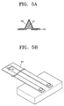
- the cantilever 52 shown in FIG. 5B itself, acts as interconnections for applying current to a tip and reading signals. Any cantilever that can apply current to the tip and read variations in current value between the tip and a storage medium can be used.
- the cantilevers 42 and 52 are formed of SiN or a dielectric material having a low stress.
- Cone-shaped tips 41 and 51 are formed at the end of the probe in a direction perpendicular to the dielectric layer 33 shown in FIGS. 3A and 3B.
- the tips 41 and 51 are formed of silicon or lightly-doped silicon.
- Each of the tips 41 and 51 is connected to a metal electrode for applying heat to the tip through each of the cantilevers 42 and 52 with two lines.
- the tips 41 and 51 are preferably coated with metal layers 44 and 53, respectively, in the case of reading data.
- FIG. 6 is a diagram of another probe according to the present invention.
- an interconnection for heating and an interconnection for measuring contact resistance are separately manufactured.
- the probe of FIG. 6 is formed to carry out the two functions, that is, heating and measuring contact resistance, at the same time.
- a first contact pad 62 and a second contact pad 63 are connected to short lines of a cantilever and the line connected to the first contact pad 62 is in contact with a tip 61 of the probe.
- the line connected to the second contact pad 63 is not in contact with the tip 61 of the probe.
- the data recording and reading principles of an apparatus for recording and reading data having the probe shown in FIG. 6 are as follows.
- recording data current is applied through the first contact pad 62 and then, heat is generated at the second contact pad 63 having a high resistance. Accordingly, it is possible to record a bit which is a data unit on a storage medium formed of polymer and placed on a substrate by melting the polymer with the heat.
- reading data the variation of contact resistance between the polymer and the tip is measured using only the first contact pad 62.
- it is not necessary to prepare each separate line for different purposes such as data recording and data reading.
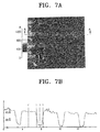
- FIG. 7A is an AFM image showing the surface of a data storage medium on which data bits are recorded using a typical probe and following the data storage mechanism of the present invention.
- FIG. 7B is a graph showing the heights of portions on the surface of the data storage medium of FIG. 7A.
- the AFM image shows a dielectric layer on which holes are formed.
- the size of the holes that is, the size of data bits depends on the size of the tip of the probe.
- FIG. 7B is a graph showing the relative height of each portion on the dielectric layer, taken along the line A - A' of FIG. 7A. As shown in this graph, the holes are formed at predetermined positions on the dielectric layer.
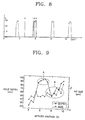
- FIG. 8 is a graph illustrating the results of applying the data reading mechanism of the present invention to the data storage medium shown in FIGS. 7A and 7B.
- a voltage of 3V is applied.
- an output voltage of 3V is measured.
- the same results as described above with reference to FIG. 8 can be achieved by applying the data recording and reading mechanisms of the present invention to a typical probe.
- FIG. 9 shows graphical results of performing a rewritable test on an apparatus for recording and reading data according to the present invention.
- the X-axis indicates voltage applied to a probe
- the left Y-axis indicates the depth of the hole
- the right Y-axis indicates the size of a pit formed by the heated probe.
- a dielectric layer that is, polymer
- the dielectric layer only acts as a passivation layer for preventing a short circuit occurring between the probe tip and metal or semiconductor and thus, the thickness of the polymer layer can be reduced to 40 nm or less. Accordingly, the size of a hole exposing the surface of the conductive layer (the metal or semiconductor layer) can be reduced significantly and the size of a data bit can be decreased, thereby enhancing the density of data recordable on a data storage medium.
- data can be read by sensing variations in temperature.
- data is read by sensing variations in the output voltage value caused by contact between the probe tip and the dielectric layer or the conductive layer, that is, sensing electric signals.
- the data read speed is only influenced by the oscillation frequency of the probe.
- the output voltage can be measured as the ratio of outer resistance to contact resistance.
- the present invention it is possible to obtain a considerable amount of output voltage without adding an amplification circuit and it is also possible to obtain a signal-to-noise ratio even higher than that of the prior art.
- the present invention does not cause the problems of the prior art in which images becomes blurred depending on distribution of temperatures.
- the present invention it is possible to solve the problems concerning data retention, a superparamagnetic limit, a signal-to-noise ratio which have been at issue in developing data storage media with the use of a conventional SPM technique. Therefore, the reliability of a subminiature storage storage device can be significantly enhanced and the structure of measurement circuits used in the storage device can be simplified, thereby reducing the cost of production.
Landscapes
- Engineering & Computer Science (AREA)
- Chemical & Material Sciences (AREA)
- Nanotechnology (AREA)
- Physics & Mathematics (AREA)
- Mathematical Physics (AREA)
- Theoretical Computer Science (AREA)
- Crystallography & Structural Chemistry (AREA)
- Semiconductor Memories (AREA)
- Length Measuring Devices With Unspecified Measuring Means (AREA)
- Measurement Of Resistance Or Impedance (AREA)
- Measuring Leads Or Probes (AREA)
Abstract
Description
Claims (16)
- An apparatus for recording and reading data comprising:characterized in that the storage medium comprises:a storage medium on which data is recorded; anda probe which is installed to face the storage medium and is used for recording data on the storage medium and reading the data recorded on the storage medium;a conductive layer (34); anda dielectric layer (33) which is formed on the conductive layer and is selectively removable to represent recorded data.
- The apparatus of claim 1, wherein holes are formed on predetermined portions of the dielectric layer so as to expose the top surface of the conductive layer.
- The apparatus of claim 1 or 2, wherein the dielectric layer is formed of one among the group consisting of a organic material, a polymer, a wax and a liquid crystal, and/or the conductive layer is formed of one among the group consisting of metal and semiconductor.
- The apparatus of any one of claims 1 to 3, further comprising a substrate (35) on which said conductive layer is formed, wherein the substrate is one of a silicon substrate, a glass substrate, and a metal substrate.
- An apparatus for recording and reading data comprising:characterized in that the storage medium further comprises:a storage medium on which data is recorded including a substrate (35); anda probe which is installed to face the storage medium and is used for recording data on the storage medium and reading data recorded on the storage medium;a conductive layer (33') which is formed on the substrate and is selectively removable to represent recorded data.
- The apparatus of claim 5, wherein the conductive layer is formed of conductive polymer.
- The apparatus of any one of claims 1 to 6, wherein the probe comprises a cantilever and a tip fixed on the cantilever.
- The apparatus of claim 7, wherein the cantilever is formed of one among the group consisting of Si, SiN and dielectric material, and/or the tip is formed of silicon and/or the surface of the tip is coated with a metal layer.
- The apparatus of claim 7 or 8, wherein the probe operates a predetermined distance apart from the storage medium or in contact with the storage medium.
- The apparatus of any one of claims 7 to 9, wherein the probe further comprises a first contact pad and a second contact pad which are connected to short lines of the cantilever, the short line connected to the first contact pad is in contact with the probe tip and the short line connected to the second contact pad is not in contact with the probe tip.
- A method for recording and reading data in an apparatus having the features of any one of claims 1 to 4 and 7 to 10,
characterized by the steps of
recording data by forming a hole on a predetermined portion of the dielectric layer to expose the surface of the conductive layer; and
reading data by scanning the surface of the storage medium with the probe and sensing the variation of output value caused by contact between the probe and the storage medium. - The method of claim 11, wherein the hole is formed by applying current to the probe to heat the tip and melting the dielectric layer with the heated tip.
- The method of claim 11 or 12, wherein variations in output voltage are caused by a short circuit between the tip and the surface of the conductive layer exposed by the hole in scanning the dielectric layer with the tip and is measured by a voltmeter included in the apparatus for recording and reading data.
- A method for recording and reading data in an apparatus having the features of any one of claims 5 to 10,
characterized by the steps of
recording data by forming a hole on a predetermined portion of the conductive layer to expose the surface of the substrate; and
reading data by scanning the surface of the storage medium with the probe and sensing variations in the output value caused by contact between the probe and the storage medium. - The method of claim 14, wherein the hole is formed by applying current to the probe to heat the tip and melting the conductive layer with the heated tip.
- The method of claim 14 or 15, wherein, if the tip encounters the hole during scanning of the conductive layer, at which the tip and the conductive layer are shorted by each other, output voltage is reduced to 0 V around the hole and variations in output voltage is measured by a voltmeter included in the apparatus for recording and reading data.
Applications Claiming Priority (2)
| Application Number | Priority Date | Filing Date | Title |
|---|---|---|---|
| KR2000072596 | 2000-12-01 | ||
| KR10-2000-0072596A KR100389903B1 (en) | 2000-12-01 | 2000-12-01 | Mass data storage and the method of writing and reading therof by contact resitance measurement |
Publications (2)
| Publication Number | Publication Date |
|---|---|
| EP1213716A2 true EP1213716A2 (en) | 2002-06-12 |
| EP1213716A3 EP1213716A3 (en) | 2004-10-13 |
Family
ID=19702579
Family Applications (1)
| Application Number | Title | Priority Date | Filing Date |
|---|---|---|---|
| EP01124829A Ceased EP1213716A3 (en) | 2000-12-01 | 2001-10-18 | Apparatus for recording and reading data and method of recording and reading data using contact resistance measurement thereof |
Country Status (4)
| Country | Link |
|---|---|
| US (1) | US6762402B2 (en) |
| EP (1) | EP1213716A3 (en) |
| JP (1) | JP3860735B2 (en) |
| KR (1) | KR100389903B1 (en) |
Cited By (3)
| Publication number | Priority date | Publication date | Assignee | Title |
|---|---|---|---|---|
| WO2004049323A1 (en) * | 2002-11-26 | 2004-06-10 | Griffith University | Nano-fabricated data storage device and operation and production methods therefor |
| EP1550846A1 (en) * | 2003-12-17 | 2005-07-06 | Hewlett-Packard Development Company, L.P. | Contact probe storage FET sensor |
| WO2006002115A2 (en) | 2004-06-17 | 2006-01-05 | Hewlett-Packard Development Company L.P. | Semiconductor storage device |
Families Citing this family (40)
| Publication number | Priority date | Publication date | Assignee | Title |
|---|---|---|---|---|
| US7260051B1 (en) | 1998-12-18 | 2007-08-21 | Nanochip, Inc. | Molecular memory medium and molecular memory integrated circuit |
| JP4771324B2 (en) * | 2001-09-10 | 2011-09-14 | パイオニア株式会社 | Dielectric information apparatus, tape-shaped medium recording / reproducing apparatus, and disk-shaped medium recording / reproducing apparatus |
| US7218600B2 (en) * | 2001-09-10 | 2007-05-15 | Pioneer Corporation | Dielectric constant measuring apparatus, dielectric constant measuring method, and information recording/reproducing apparatus |
| JP4141745B2 (en) * | 2002-06-06 | 2008-08-27 | 康雄 長 | Dielectric recording / reproducing head, dielectric recording medium unit, and dielectric recording / reproducing apparatus |
| JP3954456B2 (en) * | 2002-07-09 | 2007-08-08 | パイオニア株式会社 | Pickup device |
| JP4017104B2 (en) * | 2002-07-09 | 2007-12-05 | パイオニア株式会社 | Dielectric recording / reproducing head and tracking method |
| JP4082947B2 (en) * | 2002-07-09 | 2008-04-30 | パイオニア株式会社 | Recording / reproducing head and manufacturing method thereof |
| US7409488B2 (en) * | 2002-07-23 | 2008-08-05 | International Business Machines Inc | Data processing system |
| JP4098689B2 (en) | 2002-09-11 | 2008-06-11 | 康雄 長 | Dielectric reproducing apparatus, dielectric recording apparatus, and dielectric recording / reproducing apparatus |
| JP3701268B2 (en) * | 2002-09-11 | 2005-09-28 | 康雄 長 | Dielectric recording apparatus, dielectric reproducing apparatus, and dielectric recording / reproducing apparatus |
| US6944114B2 (en) | 2002-12-17 | 2005-09-13 | Hewlett-Packard Development Company, L.P. | Contact probe storage device including conductive readout medium |
| US6886395B2 (en) * | 2003-01-16 | 2005-05-03 | Veeco Instruments Inc. | Method of fabricating a surface probing device and probing device produced thereby |
| US20070014047A1 (en) * | 2003-05-01 | 2007-01-18 | Yasuo Cho | Recording/reproduction head and recording/reproduction device |
| JP2005004890A (en) * | 2003-06-12 | 2005-01-06 | Yasuo Cho | Data recording/reproducing device using needle-like member, and data recording/reproducing method |
| US7315505B2 (en) * | 2003-07-14 | 2008-01-01 | Hewlett-Packard Development Company, L.P. | Storage device having a probe with plural tips |
| US7215633B2 (en) * | 2003-08-13 | 2007-05-08 | Hewlett-Packard Development Company, L.P. | Storage device having a probe with a tip to form a groove in a storage medium |
| US7173314B2 (en) * | 2003-08-13 | 2007-02-06 | Hewlett-Packard Development Company, L.P. | Storage device having a probe and a storage cell with moveable parts |
| CN100379688C (en) * | 2003-08-22 | 2008-04-09 | Fmc福瑞特股份有限公司 | Method, device and reagent for wastewater purification |
| JP4326007B2 (en) | 2003-08-25 | 2009-09-02 | 康雄 長 | Signal detecting method and apparatus, and information reproducing apparatus and method |
| US7329361B2 (en) * | 2003-10-29 | 2008-02-12 | International Business Machines Corporation | Method and apparatus for fabricating or altering microstructures using local chemical alterations |
| US7391706B2 (en) * | 2003-10-31 | 2008-06-24 | Samsung Electronics Co., Ltd. | Data storage device including conductive probe and ferroelectric storage medium |
| JP4145773B2 (en) * | 2003-11-06 | 2008-09-03 | パイオニア株式会社 | Information recording / reproducing apparatus and recording medium |
| EP1544859A1 (en) * | 2003-12-17 | 2005-06-22 | Hewlett-Packard Development Company, L.P. | Read/write arrangements for probes |
| US7460462B2 (en) * | 2003-12-17 | 2008-12-02 | Hewlett-Packard Development Company, L.P. | Contact probe storage fet sensor and write heater arrangements |
| KR20050065902A (en) * | 2003-12-26 | 2005-06-30 | 한국전자통신연구원 | Method for fabricating nano pore |
| US6999403B2 (en) * | 2004-04-02 | 2006-02-14 | Hewlett-Packard Development Company, L.P. | Storage device having a probe to cooperate with a storage medium to provide a variable resistance |
| DE602005024312D1 (en) * | 2004-08-18 | 2010-12-02 | Us Gov Navy Naval Res Lab | HEAT CONTROL OF DEPOSITION IN DPN (DIP-PEN-NANOLITHOGRAPHY) |
| US7463573B2 (en) | 2005-06-24 | 2008-12-09 | Nanochip, Inc. | Patterned media for a high density data storage device |
| US20070041238A1 (en) * | 2005-07-08 | 2007-02-22 | Nanochip, Inc. | High density data storage devices with read/write probes with hollow or reinforced tips |
| KR100648041B1 (en) * | 2005-07-14 | 2006-11-23 | 전자부품연구원 | Data storage device using scanning probe microscope |
| US20080074792A1 (en) * | 2006-09-21 | 2008-03-27 | Nanochip, Inc. | Control scheme for a memory device |
| US7913544B1 (en) | 2006-11-15 | 2011-03-29 | Applied Nanostructures, Inc. | Scanning probe devices and methods for fabricating same |
| US7928343B2 (en) * | 2007-12-04 | 2011-04-19 | The Board Of Trustees Of The University Of Illinois | Microcantilever heater-thermometer with integrated temperature-compensated strain sensor |
| WO2009097487A1 (en) * | 2008-01-31 | 2009-08-06 | The Board Of Trustees Of The University Of Illinois | Temperature-dependent nanoscale contact potential measurement technique and device |
| US8931950B2 (en) | 2008-08-20 | 2015-01-13 | The Board Of Trustees Of The University Of Illinois | Device for calorimetric measurement |
| US8387443B2 (en) * | 2009-09-11 | 2013-03-05 | The Board Of Trustees Of The University Of Illinois | Microcantilever with reduced second harmonic while in contact with a surface and nano scale infrared spectrometer |
| US8533861B2 (en) | 2011-08-15 | 2013-09-10 | The Board Of Trustees Of The University Of Illinois | Magnetic actuation and thermal cantilevers for temperature and frequency dependent atomic force microscopy |
| US8914911B2 (en) | 2011-08-15 | 2014-12-16 | The Board Of Trustees Of The University Of Illinois | Magnetic actuation and thermal cantilevers for temperature and frequency dependent atomic force microscopy |
| CN104094349B (en) * | 2011-12-05 | 2016-08-24 | 瓦里安半导体设备公司 | Write head, magnetic storage device and method for recording data in magnetic storage device |
| US11994545B2 (en) | 2021-05-11 | 2024-05-28 | National Instruments Corporation | DC resistance measurement contact checking via alternating current high frequency injection |
Family Cites Families (19)
| Publication number | Priority date | Publication date | Assignee | Title |
|---|---|---|---|---|
| GB1088117A (en) * | 1965-11-10 | 1967-10-25 | Standard Telephones Cables Ltd | Recording on a moving medium |
| JP2756254B2 (en) * | 1988-03-25 | 1998-05-25 | キヤノン株式会社 | Recording device and playback device |
| US5138174A (en) * | 1991-07-16 | 1992-08-11 | E. I. Du Pont De Nemours And Company | Nanometer-scale structures and lithography |
| JP3060143B2 (en) * | 1992-07-31 | 2000-07-10 | キヤノン株式会社 | Recording medium and information processing apparatus using the same |
| FR2695384B1 (en) * | 1992-09-04 | 1994-12-09 | Corning Inc | Method for improving the fixing using a fiber optic adhesive to a glass substrate, and integrated optical component treated by this method. |
| US5323377A (en) * | 1992-11-27 | 1994-06-21 | Chen Zhi Q | Electrical data recording and retrieval based on impedance variation |
| EP0615235B9 (en) * | 1993-03-09 | 2003-11-12 | Canon Kabushiki Kaisha | Information recording method and information recording apparatus |
| JPH08212604A (en) * | 1994-01-31 | 1996-08-20 | Matsushita Electric Ind Co Ltd | Information recording / reproducing apparatus and information recording / reproducing method |
| KR950024146A (en) * | 1994-01-31 | 1995-08-21 | 모리시타 요이찌 | Information recording and reproducing apparatus and information recording and reproducing method |
| US5751683A (en) * | 1995-07-24 | 1998-05-12 | General Nanotechnology, L.L.C. | Nanometer scale data storage device and associated positioning system |
| JPH0862230A (en) * | 1994-08-24 | 1996-03-08 | Olympus Optical Co Ltd | Integration type spm sensor |
| JPH08297870A (en) * | 1995-04-26 | 1996-11-12 | Canon Inc | Information processing apparatus and information processing method |
| JPH08315434A (en) * | 1995-05-18 | 1996-11-29 | Canon Inc | Information processing device |
| JP3576644B2 (en) * | 1995-06-19 | 2004-10-13 | キヤノン株式会社 | Probe and recording medium of information recording apparatus, and information recording method using these |
| JPH1040599A (en) * | 1996-07-25 | 1998-02-13 | Tdk Corp | Recording medium and recording reproducing method |
| JPH10106053A (en) * | 1996-10-02 | 1998-04-24 | Matsushita Electric Ind Co Ltd | Information recording medium, method of manufacturing the same, information recording method and information recording apparatus using the same |
| WO2004074765A1 (en) * | 1997-07-17 | 2004-09-02 | Gerd Karl Binnig | Method of forming ultrasmall structures and apparatus therefor |
| US6477132B1 (en) * | 1998-08-19 | 2002-11-05 | Canon Kabushiki Kaisha | Probe and information recording/reproduction apparatus using the same |
| US6181097B1 (en) * | 1999-02-11 | 2001-01-30 | Institute Of Materials Research And Engineering | High precision three-dimensional alignment system for lithography, fabrication and inspection |
-
2000
- 2000-12-01 KR KR10-2000-0072596A patent/KR100389903B1/en not_active Expired - Fee Related
-
2001
- 2001-10-11 US US09/973,869 patent/US6762402B2/en not_active Expired - Fee Related
- 2001-10-15 JP JP2001316332A patent/JP3860735B2/en not_active Expired - Fee Related
- 2001-10-18 EP EP01124829A patent/EP1213716A3/en not_active Ceased
Cited By (4)
| Publication number | Priority date | Publication date | Assignee | Title |
|---|---|---|---|---|
| WO2004049323A1 (en) * | 2002-11-26 | 2004-06-10 | Griffith University | Nano-fabricated data storage device and operation and production methods therefor |
| EP1550846A1 (en) * | 2003-12-17 | 2005-07-06 | Hewlett-Packard Development Company, L.P. | Contact probe storage FET sensor |
| WO2006002115A2 (en) | 2004-06-17 | 2006-01-05 | Hewlett-Packard Development Company L.P. | Semiconductor storage device |
| WO2006002115A3 (en) * | 2004-06-17 | 2006-03-23 | Hewlett Packard Development Co | Semiconductor storage device |
Also Published As
| Publication number | Publication date |
|---|---|
| US6762402B2 (en) | 2004-07-13 |
| JP2002184051A (en) | 2002-06-28 |
| EP1213716A3 (en) | 2004-10-13 |
| KR100389903B1 (en) | 2003-07-04 |
| US20020066855A1 (en) | 2002-06-06 |
| KR20020043119A (en) | 2002-06-08 |
| JP3860735B2 (en) | 2006-12-20 |
Similar Documents
| Publication | Publication Date | Title |
|---|---|---|
| US6762402B2 (en) | Apparatus for recording and reading data and method of recording and reading data using contact resistance measurement thereof | |
| US5856672A (en) | Single-crystal silicon cantilever with integral in-plane tip for use in atomic force microscope system | |
| JP4192146B2 (en) | A semiconductor probe having a resistive chip and a manufacturing method thereof, an information recording device, an information reproducing device and an information measuring device having the same. | |
| JP3073616B2 (en) | Information processing device with multiple probes | |
| US6665258B1 (en) | Method and apparatus for recording, storing and reproducing information | |
| US5729026A (en) | Atomic force microscope system with angled cantilever having integral in-plane tip | |
| KR20050083759A (en) | Phase change media for high density data storage | |
| US7233517B2 (en) | Atomic probes and media for high density data storage | |
| US7167435B2 (en) | Storage device having a probe with plural tips | |
| JP2008021407A (en) | Data storage method and data storage device | |
| JP4642236B2 (en) | Information medium writing and reading method, and recording medium | |
| JP2006078485A (en) | Semiconductor probe with resistive tip and method for manufacturing the same | |
| CN100517479C (en) | Contact probe storage device including conductive readout medium | |
| CN100587853C (en) | Method of making semiconductor probe with resistive tip | |
| US7539119B2 (en) | Data storage apparatus using current switching in metal oxide layer | |
| JP2000348397A (en) | Information medium, information reproducing method and information reproducing device | |
| KR100499125B1 (en) | Apparatus and method for reproducing data using capacitance vatiation | |
| US8374071B2 (en) | Data storage device | |
| KR100634552B1 (en) | Field sensing probe with separated sensor and information storage device with same | |
| KR20070108026A (en) | Scanning probe microscopy information storage device and manufacturing method thereof | |
| KR100519221B1 (en) | Cantilever of variable conductivity type and manufacturing method thereof, for use in nano data storage device | |
| KR100746769B1 (en) | Cantilever for storing information, information storage device having same, and manufacturing method | |
| JPH07110969A (en) | Face alignment method, position control mechanism and information processor with the mechanism | |
| JP2001184751A (en) | Recording / reproducing method, optical recording / reproducing device, and optical recording medium | |
| US20080025191A1 (en) | Data storage device |
Legal Events
| Date | Code | Title | Description |
|---|---|---|---|
| PUAI | Public reference made under article 153(3) epc to a published international application that has entered the european phase |
Free format text: ORIGINAL CODE: 0009012 |
|
| AK | Designated contracting states |
Kind code of ref document: A2 Designated state(s): AT BE CH CY DE DK ES FI FR GB GR IE IT LI LU MC NL PT SE TR |
|
| AX | Request for extension of the european patent |
Free format text: AL;LT;LV;MK;RO;SI |
|
| PUAL | Search report despatched |
Free format text: ORIGINAL CODE: 0009013 |
|
| AK | Designated contracting states |
Kind code of ref document: A3 Designated state(s): AT BE CH CY DE DK ES FI FR GB GR IE IT LI LU MC NL PT SE TR |
|
| AX | Request for extension of the european patent |
Extension state: AL LT LV MK RO SI |
|
| 17P | Request for examination filed |
Effective date: 20050314 |
|
| AKX | Designation fees paid |
Designated state(s): CH DE LI |
|
| 17Q | First examination report despatched |
Effective date: 20070829 |
|
| RAP1 | Party data changed (applicant data changed or rights of an application transferred) |
Owner name: SAMSUNG ELECTRONICS CO., LTD. |
|
| STAA | Information on the status of an ep patent application or granted ep patent |
Free format text: STATUS: THE APPLICATION HAS BEEN REFUSED |
|
| 18R | Application refused |
Effective date: 20141105 |