EP1213682A2 - Print image enhancement in LED array xerographic printing - Google Patents
Print image enhancement in LED array xerographic printing Download PDFInfo
- Publication number
- EP1213682A2 EP1213682A2 EP01128420A EP01128420A EP1213682A2 EP 1213682 A2 EP1213682 A2 EP 1213682A2 EP 01128420 A EP01128420 A EP 01128420A EP 01128420 A EP01128420 A EP 01128420A EP 1213682 A2 EP1213682 A2 EP 1213682A2
- Authority
- EP
- European Patent Office
- Prior art keywords
- image
- pixels
- photoreceptor
- exposure
- pixel
- Prior art date
- Legal status (The legal status is an assumption and is not a legal conclusion. Google has not performed a legal analysis and makes no representation as to the accuracy of the status listed.)
- Granted
Links
Images


Classifications
-
- G—PHYSICS
- G06—COMPUTING OR CALCULATING; COUNTING
- G06K—GRAPHICAL DATA READING; PRESENTATION OF DATA; RECORD CARRIERS; HANDLING RECORD CARRIERS
- G06K15/00—Arrangements for producing a permanent visual presentation of the output data, e.g. computer output printers
- G06K15/02—Arrangements for producing a permanent visual presentation of the output data, e.g. computer output printers using printers
- G06K15/12—Arrangements for producing a permanent visual presentation of the output data, e.g. computer output printers using printers by photographic printing, e.g. by laser printers
- G06K15/1238—Arrangements for producing a permanent visual presentation of the output data, e.g. computer output printers using printers by photographic printing, e.g. by laser printers simultaneously exposing more than one point
- G06K15/1242—Arrangements for producing a permanent visual presentation of the output data, e.g. computer output printers using printers by photographic printing, e.g. by laser printers simultaneously exposing more than one point on one main scanning line
- G06K15/1247—Arrangements for producing a permanent visual presentation of the output data, e.g. computer output printers using printers by photographic printing, e.g. by laser printers simultaneously exposing more than one point on one main scanning line using an array of light sources, e.g. a linear array
Definitions
- Some xerographic printers operate in a "write black” mode to optically expose the image foreground for printing by means of an "exposed area development” process, while others operate in a “write white” mode to expose the image background for printing by means of a “charged area development” process.
- the converting includes illuminating a portion of the charge retentive surface with: a first spot size for data assigned with the altered exposure value, and a second spot size smaller than the first spot size for data assigned with other than the altered exposure value.
- One advantage of the present invention resides in the identification, in real time, of image characteristics which are enhanced from selective altered exposure.
- the LED array 38 is disposed across the photoreceptor 36 in the fast scan direction.
- the photoreceptor 36 is advanced (by means not shown) simultaneously in an orthogonal, process direction at a substantially constant linear velocity, as indicated by the arrow 42 , so the array of beams 32 exposes the photoreceptor 36 in successive raster-like scan lines.
- the photoreceptor 36 is coated on a rotating drum, but it will be apparent that it also could be carried by a belt or any other suitable substrate.
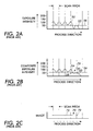
- each of the line-like exposure profiles that the image bar 38 prints on the photoreceptor 36 is composed of multiple, superpositioned, discrete exposures that have contrast levels which vary in accordance with the output intensities of the respective LED's by which they were printed.
- LED bars typically comprise projection optics 40 which cause the center-to-center spacing of these superpositioned exposures to be substantially greater than the effective diameter of the individual print spots that are produced by the LEDs.
- the optical aperture of the LED array 38 is sufficiently large to avoid excessive truncation of the light beam 32 because the beam 32 then comes to a generally circular or elliptical focus with a gaussian intensity profile.
- the broader aspects of this invention are not limited to any specific scan spot geometry or intensity profile. Accepted design principles indicate that the spatial frequency power spectrum of the scan spot profile should not have significant spatial frequency components outside the spatial frequency passband of the imaging system, but the scan spot can otherwise be tailored to satisfy a variety of system requirements.
- the processor 20 hence the light beam 32 variably exposes the photoreceptor 36 .
- amplitude, duty cycle, pulse width, number and location of high addressable bits and/or timing of illumination, as well as combinations of the preceding are modulated (collectively referred to herein as "variably exposed” or a variant thereof) in accordance with successive multi-bit digital data values and particularly in response to surrounding pixels and identified image characteristics.
- These data values are optionally clocked out of rendering processor 20 serially or in parallel in response to data clock pulses which are time synchronized.
- rendering processor 20 or other means may preprocess the data for the printing of halftoned pixels, contone pixels, negative signals, text, line art and/or other corrections.
- the fast scan pixel positioning precision of the print engine 10 can be enhanced, if desired, by means of systems such as those described in the following commonly assigned United States Patents (hereby incorporated by reference): D. N. Curry U.S. Pat. No. 4,622,593 which issued Nov. 11, 1986 on “Polygon Signature Correction”; D. N. Curry U.S. Pat. No. 4,639,789 which issued Jan. 27, 1987 on “Raster Scanner Variable-Frequency Clock Circuit”; D. N. Curry et al. U. S. Pat. No. 4,766,560 which issued Aug. 23, 1988 on “Parallel/Pipelined Arithmetic Variable Clock Frequency Synthesizer”; D. N. Curry U.
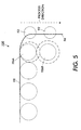
- Figure 5 illustrates an exemplary solution to the above described deficiency.
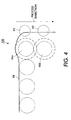
- the overexposed "pre-boundary" pixels 106A , 106B border the "boundary" scan pixels 92 to define the vertical edge 96 offset in the fast-scan direction.
- pixel 106A is determined to occupy the corner and special variable exposure processing is applied. In this case, pixel 106A is imaged temporally offset or delayed, and is thus spatially displaced with respect to the photodetector 36 and other pixels in the scan-line.
Landscapes
- Physics & Mathematics (AREA)
- Engineering & Computer Science (AREA)
- Optics & Photonics (AREA)
- General Engineering & Computer Science (AREA)
- General Physics & Mathematics (AREA)
- Theoretical Computer Science (AREA)
- Printers Or Recording Devices Using Electromagnetic And Radiation Means (AREA)
- Fax Reproducing Arrangements (AREA)
- Color, Gradation (AREA)
- Exposure Or Original Feeding In Electrophotography (AREA)
- Control Or Security For Electrophotography (AREA)
Abstract
Description
Claims (10)
- A method of xerographic digital imaging where an LED bar selectively exposes an area of a photoreceptor in response to an input, the method comprising:receiving a plurality of pixels, representing an input pixel; andvarying an exposure on the photoreceptor of a selected pixel based on surrounding pixels, the selected pixel exposing an area on the photoreceptor different than other pixels.
- The method of imaging as set forth in claim 1, further comprising parsing the plurality of input pixels for a determined image characteristic.
- The method of imaging as set forth in claim 2, where the parsing comprises template matching the plurality of image pixels.
- The method of imaging as set forth in claim 2, where a set of the image pixels are exposed at a reference level, the varying step comprising:based on the parsing, selecting a pixel comprising the determined image characteristic for varied exposure; andvariably exposing the selected pixel relative to the reference level.
- The method of imaging as set forth in claim 1, the varying step comprising:delaying exposing of the photoreceptor for the selected pixel.
- The method of imaging as set forth in claim 1, the varying step comprising:ceasing exposing the photoreceptor for the selected pixel prior to other pixels.
- The method of imaging as set forth in claim 1, where the varying step comprises altering the exposure of the photoreceptor for selected pixels comprising identifiable image structures.
- An xerographic printing apparatus comprising:an input which receives digital pixels representing an input image;a processor which processes the pixel and directs signals to an LED bar which selectively exposes areas of a photoreceptor to produce a latent image, the processor controlling exposure of the photoreceptor by variably exposing a selected pixel based on surrounding pixels; and,an image output which converts the latent image on the photoreceptor to an image on an output media.
- The imaging apparatus as set forth in claim 8, where the processor comprises:an image structure parser which examines the pixels to determine an image structure beneficially adaptable to varied exposure;an image pixel selector which analyzes pixels comprising the determined image structure and selects a pixel for varied exposure; and,an exposure calculator which determines a variable exposure relative to a reference for at least the selected pixel.
- A method of digital imaging where a digital image is processed and output on a printing device including an image bar disposed across a charge retentive surface, the method comprising:parsing an input data sequence representative of the digital image until a determined condition is encountered; andassigning a varied exposure value to a datum in the input sequence based on adjacency to the determined condition.
Applications Claiming Priority (2)
| Application Number | Priority Date | Filing Date | Title |
|---|---|---|---|
| US09/731,120 US6985627B2 (en) | 2000-12-06 | 2000-12-06 | LED bar array high addressable imaging in 2-dimensions |
| US731120 | 2000-12-06 |
Publications (3)
| Publication Number | Publication Date |
|---|---|
| EP1213682A2 true EP1213682A2 (en) | 2002-06-12 |
| EP1213682A3 EP1213682A3 (en) | 2004-01-07 |
| EP1213682B1 EP1213682B1 (en) | 2010-03-03 |
Family
ID=24938145
Family Applications (1)
| Application Number | Title | Priority Date | Filing Date |
|---|---|---|---|
| EP01128420A Expired - Lifetime EP1213682B1 (en) | 2000-12-06 | 2001-12-04 | Print image enhancement in LED array xerographic printing |
Country Status (4)
| Country | Link |
|---|---|
| US (1) | US6985627B2 (en) |
| EP (1) | EP1213682B1 (en) |
| JP (1) | JP2002234208A (en) |
| DE (1) | DE60141447D1 (en) |
Families Citing this family (8)
| Publication number | Priority date | Publication date | Assignee | Title |
|---|---|---|---|---|
| US7236272B2 (en) * | 2001-08-03 | 2007-06-26 | Transpacific Ip, Ltd. | Compensation apparatus for image scan |
| US7957007B2 (en) * | 2006-05-17 | 2011-06-07 | Mitsubishi Electric Research Laboratories, Inc. | Apparatus and method for illuminating a scene with multiplexed illumination for motion capture |
| US9347642B2 (en) | 2011-09-07 | 2016-05-24 | Terralux, Inc. | Faceted optics for illumination devices |
| US9470406B2 (en) | 2012-09-24 | 2016-10-18 | Terralux, Inc. | Variable-beam light source and related methods |
| WO2015006478A1 (en) | 2013-07-09 | 2015-01-15 | Terralux, Inc. | Variable-beam light source and related methods |
| US10072819B2 (en) | 2014-10-02 | 2018-09-11 | Ledvance Llc | Light source for uniform illumination of a surface |
| US10036535B2 (en) | 2014-11-03 | 2018-07-31 | Ledvance Llc | Illumination device with adjustable curved reflector portions |
| US10405388B2 (en) | 2014-12-11 | 2019-09-03 | Ledvance Llc | Variable-beam light source with mixing chamber |
Family Cites Families (22)
| Publication number | Priority date | Publication date | Assignee | Title |
|---|---|---|---|---|
| US5027158A (en) * | 1987-12-18 | 1991-06-25 | Colorocs Corporation | Vertical print engine for electrophotographic apparatus |
| JP2568713B2 (en) * | 1987-12-23 | 1997-01-08 | 松下電器産業株式会社 | Electrophotographic forming method |
| US5131053A (en) * | 1988-08-10 | 1992-07-14 | Caere Corporation | Optical character recognition method and apparatus |
| US4970554A (en) * | 1988-10-24 | 1990-11-13 | Xerox Corporation | Job processing system for high speed electronic copying/printing machines |
| US5053818A (en) * | 1990-12-19 | 1991-10-01 | Xerox Corporation | Method and apparatus for copying semi-transparent originals using a black backing member |
| JP2866758B2 (en) | 1991-07-05 | 1999-03-08 | 沖電気工業株式会社 | Non-impact printer |
| US5430472A (en) | 1991-07-29 | 1995-07-04 | Xerox Corporation | Method and apparatus for eliminating distortion via overscanned illumination for optical printers and the like having high gamma photosensitive recording media and high addressability |
| US5367381A (en) | 1991-07-29 | 1994-11-22 | Xerox Corporation | Method and apparatus for enhanced resolution and contrast via super intensity controlled overscanned illumination in a two dimensional high addressability printer |
| US5274472A (en) | 1992-05-21 | 1993-12-28 | Xerox Corporation | High addressability image generator using pseudo interpolation of video and screen data |
| US5455681A (en) | 1992-11-16 | 1995-10-03 | Eastman Kodak Company | Low resolution grey level printing method from high resolution binary input file |
| US5327524A (en) | 1992-12-28 | 1994-07-05 | Eastman Kodak Company | Electrophotographic recording with multiple-bit grey level LED printhead with enhanced addressability |
| JPH0789128A (en) | 1993-07-30 | 1995-04-04 | Kyocera Corp | High-density image forming method in LED printer |
| US5774165A (en) | 1994-09-22 | 1998-06-30 | Oki Electric Industry Co., Ltd. | Light emission intensity width compensating method of LED print head and apparatus thereof |
| US5623714A (en) * | 1994-11-23 | 1997-04-22 | Xerox Corporation | Automatic exposure correction using current sensing technology |
| US5606648A (en) | 1994-12-08 | 1997-02-25 | Xerox Corporation | Apparatus and method for modulating image signals in a high addressability printing machine |
| US5900901A (en) * | 1995-06-05 | 1999-05-04 | Xerox Corporation | Method and apparatus for compensating for raster position errors in output scanners |
| JP3082645B2 (en) | 1995-10-20 | 2000-08-28 | 富士ゼロックス株式会社 | Image forming device |
| US5659399A (en) * | 1995-11-30 | 1997-08-19 | Xerox Corporation | Method for controlling compact dot growth |
| US5748330A (en) * | 1997-05-05 | 1998-05-05 | Xerox Corporation | Method of calibrating a digital printer using component test patches and the yule-nielsen equation |
| US5920683A (en) | 1997-06-27 | 1999-07-06 | Xerox Corporation | Image enhancement system for high addressability printing |
| US6452696B1 (en) * | 1998-05-01 | 2002-09-17 | Zbe Incorporated | Method and apparatus for controlling multiple light sources in a digital printer |
| US6538677B1 (en) * | 2000-05-17 | 2003-03-25 | Heidelberger Druckmaschinen Ag | Apparatus and method for gray level printing |
-
2000
- 2000-12-06 US US09/731,120 patent/US6985627B2/en not_active Expired - Fee Related
-
2001
- 2001-11-29 JP JP2001363651A patent/JP2002234208A/en active Pending
- 2001-12-04 DE DE60141447T patent/DE60141447D1/en not_active Expired - Lifetime
- 2001-12-04 EP EP01128420A patent/EP1213682B1/en not_active Expired - Lifetime
Also Published As
| Publication number | Publication date |
|---|---|
| US20020067512A1 (en) | 2002-06-06 |
| EP1213682B1 (en) | 2010-03-03 |
| US6985627B2 (en) | 2006-01-10 |
| EP1213682A3 (en) | 2004-01-07 |
| DE60141447D1 (en) | 2010-04-15 |
| JP2002234208A (en) | 2002-08-20 |
Similar Documents
| Publication | Publication Date | Title |
|---|---|---|
| EP0526000B1 (en) | Microaddressability via overscanned illumination for optical printers and the like having high gamma photosensitive recording media | |
| EP0768792B1 (en) | Method and apparatus for the resolution enhancement of gray scale images that include text and line art | |
| EP0549314B1 (en) | Enhanced fidelity reproduction of images by hierarchical template matching | |
| US5383036A (en) | Enhancement of multiple color images without color separation error by inverse symmetrical template matching | |
| US5430472A (en) | Method and apparatus for eliminating distortion via overscanned illumination for optical printers and the like having high gamma photosensitive recording media and high addressability | |
| US6332044B1 (en) | System and method for enhancement of image contour fidelity | |
| JP2000032266A (en) | Half-tone hybrid screen generating device | |
| EP0585043B1 (en) | Method and system for enhanced fidelity reproduction of images | |
| US6816269B1 (en) | Method and apparatus for electronic registration in a binary image path | |
| US6608701B1 (en) | Compact high addressability rendering | |
| US6985627B2 (en) | LED bar array high addressable imaging in 2-dimensions | |
| EP0893780B1 (en) | Method for resolution conversion of print data for a printer | |
| JPH09174931A (en) | Method for increasing dot of image | |
| US7292372B2 (en) | Image processing apparatus and image forming apparatus which adaptively switches image processing methods between a dot image portion and a non-dot image portion | |
| US5367381A (en) | Method and apparatus for enhanced resolution and contrast via super intensity controlled overscanned illumination in a two dimensional high addressability printer | |
| EP0676714B1 (en) | Exposure controlling method and apparatus in a laser printer | |
| US5321433A (en) | Electrophotographic printing apparatus with enhanced printed image capability | |
| US5818504A (en) | Adjustment of dot size for laser imagers | |
| JPH0691930A (en) | Method and device for improving resolution and contrast of optical printer | |
| JPH032773A (en) | Image forming device |
Legal Events
| Date | Code | Title | Description |
|---|---|---|---|
| PUAI | Public reference made under article 153(3) epc to a published international application that has entered the european phase |
Free format text: ORIGINAL CODE: 0009012 |
|
| AK | Designated contracting states |
Kind code of ref document: A2 Designated state(s): AT BE CH CY DE DK ES FI FR GB GR IE IT LI LU MC NL PT SE TR |
|
| AX | Request for extension of the european patent |
Free format text: AL;LT;LV;MK;RO;SI |
|
| PUAL | Search report despatched |
Free format text: ORIGINAL CODE: 0009013 |
|
| AK | Designated contracting states |
Kind code of ref document: A3 Designated state(s): AT BE CH CY DE DK ES FI FR GB GR IE IT LI LU MC NL PT SE TR |
|
| AX | Request for extension of the european patent |
Extension state: AL LT LV MK RO SI |
|
| 17P | Request for examination filed |
Effective date: 20040707 |
|
| AKX | Designation fees paid |
Designated state(s): DE FR GB |
|
| 17Q | First examination report despatched |
Effective date: 20071227 |
|
| GRAP | Despatch of communication of intention to grant a patent |
Free format text: ORIGINAL CODE: EPIDOSNIGR1 |
|
| GRAS | Grant fee paid |
Free format text: ORIGINAL CODE: EPIDOSNIGR3 |
|
| GRAA | (expected) grant |
Free format text: ORIGINAL CODE: 0009210 |
|
| AK | Designated contracting states |
Kind code of ref document: B1 Designated state(s): DE FR GB |
|
| REG | Reference to a national code |
Ref country code: GB Ref legal event code: FG4D |
|
| REF | Corresponds to: |
Ref document number: 60141447 Country of ref document: DE Date of ref document: 20100415 Kind code of ref document: P |
|
| PLBE | No opposition filed within time limit |
Free format text: ORIGINAL CODE: 0009261 |
|
| STAA | Information on the status of an ep patent application or granted ep patent |
Free format text: STATUS: NO OPPOSITION FILED WITHIN TIME LIMIT |
|
| 26N | No opposition filed |
Effective date: 20101206 |
|
| PGFP | Annual fee paid to national office [announced via postgrant information from national office to epo] |
Ref country code: DE Payment date: 20131121 Year of fee payment: 13 Ref country code: GB Payment date: 20131125 Year of fee payment: 13 |
|
| PGFP | Annual fee paid to national office [announced via postgrant information from national office to epo] |
Ref country code: FR Payment date: 20131219 Year of fee payment: 13 |
|
| REG | Reference to a national code |
Ref country code: DE Ref legal event code: R119 Ref document number: 60141447 Country of ref document: DE |
|
| GBPC | Gb: european patent ceased through non-payment of renewal fee |
Effective date: 20141204 |
|
| REG | Reference to a national code |
Ref country code: FR Ref legal event code: ST Effective date: 20150831 |
|
| PG25 | Lapsed in a contracting state [announced via postgrant information from national office to epo] |
Ref country code: DE Free format text: LAPSE BECAUSE OF NON-PAYMENT OF DUE FEES Effective date: 20150701 Ref country code: GB Free format text: LAPSE BECAUSE OF NON-PAYMENT OF DUE FEES Effective date: 20141204 |
|
| PG25 | Lapsed in a contracting state [announced via postgrant information from national office to epo] |
Ref country code: FR Free format text: LAPSE BECAUSE OF NON-PAYMENT OF DUE FEES Effective date: 20141231 |