EP1211723A2 - Optimized metal fuse process in semiconductor device - Google Patents
Optimized metal fuse process in semiconductor device Download PDFInfo
- Publication number
- EP1211723A2 EP1211723A2 EP01000649A EP01000649A EP1211723A2 EP 1211723 A2 EP1211723 A2 EP 1211723A2 EP 01000649 A EP01000649 A EP 01000649A EP 01000649 A EP01000649 A EP 01000649A EP 1211723 A2 EP1211723 A2 EP 1211723A2
- Authority
- EP
- European Patent Office
- Prior art keywords
- oxide layer
- fuses
- depositing
- oxide
- over
- Prior art date
- Legal status (The legal status is an assumption and is not a legal conclusion. Google has not performed a legal analysis and makes no representation as to the accuracy of the status listed.)
- Granted
Links
Images

Classifications
-
- H—ELECTRICITY
- H10—SEMICONDUCTOR DEVICES; ELECTRIC SOLID-STATE DEVICES NOT OTHERWISE PROVIDED FOR
- H10W—GENERIC PACKAGES, INTERCONNECTIONS, CONNECTORS OR OTHER CONSTRUCTIONAL DETAILS OF DEVICES COVERED BY CLASS H10
- H10W20/00—Interconnections in chips, wafers or substrates
- H10W20/40—Interconnections external to wafers or substrates, e.g. back-end-of-line [BEOL] metallisations or vias connecting to gate electrodes
- H10W20/49—Adaptable interconnections, e.g. fuses or antifuses
- H10W20/493—Fuses, i.e. interconnections changeable from conductive to non-conductive
- H10W20/494—Fuses, i.e. interconnections changeable from conductive to non-conductive changeable by the use of an external beam, e.g. laser beam or ion beam
-
- Y—GENERAL TAGGING OF NEW TECHNOLOGICAL DEVELOPMENTS; GENERAL TAGGING OF CROSS-SECTIONAL TECHNOLOGIES SPANNING OVER SEVERAL SECTIONS OF THE IPC; TECHNICAL SUBJECTS COVERED BY FORMER USPC CROSS-REFERENCE ART COLLECTIONS [XRACs] AND DIGESTS
- Y10—TECHNICAL SUBJECTS COVERED BY FORMER USPC
- Y10T—TECHNICAL SUBJECTS COVERED BY FORMER US CLASSIFICATION
- Y10T29/00—Metal working
- Y10T29/49—Method of mechanical manufacture
- Y10T29/49002—Electrical device making
- Y10T29/49107—Fuse making
-
- Y—GENERAL TAGGING OF NEW TECHNOLOGICAL DEVELOPMENTS; GENERAL TAGGING OF CROSS-SECTIONAL TECHNOLOGIES SPANNING OVER SEVERAL SECTIONS OF THE IPC; TECHNICAL SUBJECTS COVERED BY FORMER USPC CROSS-REFERENCE ART COLLECTIONS [XRACs] AND DIGESTS
- Y10—TECHNICAL SUBJECTS COVERED BY FORMER USPC
- Y10T—TECHNICAL SUBJECTS COVERED BY FORMER US CLASSIFICATION
- Y10T29/00—Metal working
- Y10T29/49—Method of mechanical manufacture
- Y10T29/49002—Electrical device making
- Y10T29/49117—Conductor or circuit manufacturing
- Y10T29/49124—On flat or curved insulated base, e.g., printed circuit, etc.
- Y10T29/49155—Manufacturing circuit on or in base
- Y10T29/49156—Manufacturing circuit on or in base with selective destruction of conductive paths
Definitions
- the invention is generally related to the field of semiconductor processing and more specifically to a metal fuse process.
- alternate interconnect paths are created to increase yield.
- the functionality of the device is measured.
- Defective interconnect paths are severed and replaced with alternative interconnect paths.
- the defective interconnect paths are severed by "blowing" a fuse.
- a high power laser is directed at fuses that need to be removed.
- the fuse is for the most part, vaporized by the high power laser pulse.
- a wet etch is then used to remove any remaining fuse material from the blown fuse link as well as material from the fuse that may have been redeposited on the surface during the blowing process.
- FIGs. 1A-1D One prior art fuse process is shown in FIGs. 1A-1D.
- the top metal interconnect layer is used to form both fuses, like fuse 30 and probe pads, like probe pad 40.
- the top metal interconnect comprises aluminum 42 with an overlying TiN barrier layer 44.
- 8000 ⁇ of oxide 52 are deposited using a high-density plasma (HDP) process.
- a resist pattern 54 is formed exposing the areas of oxide 52 over both the fuses and the probe pads, as shown in FIG. 1A.
- a single etch is then used to expose the fuses 30 and probe pads 40, as shown in FIG. 1B.
- An etch chemistry is used that etches both oxide and TiN. As a result of the etch and overetch required to ensure that all desired areas across the wafer are cleared, the fuse links 30 are degraded.
- circuits are then probed to determine which fuse links should be blown to fix defective circuits.
- a 3000 ⁇ conformal oxide layer 56 is deposited over the structure, as shown in FIG. 1C.
- Layer 56 completely covers the exposed fuses 30 and provides protection for the exposed aluminum of the probe pads 40.
- a laser pulse is then directed towards the fuses that need to be removed.
- the fuse 30 cracks or breaks off at the weakest point, as shown in FIG. 1D.
- a wet etch is then used to wash away any remaining broken fuses and debris and dissolve fuse links that may be still attached through cracks in the conformal oxide.
- the invention provides a metal fuse process that uses a thinner (e.g., 6000 ⁇ ) oxide over the top interconnect. Because the oxide is thin at the upper corners of the fuse, the oxide cracks over the fuse during a laser pulse. A wet etch is then used to dissolve the exposed fuses.
- thinner oxide e.g., 6000 ⁇
- An advantage of the invention is providing a metal fuse process the offers improved yield by avoiding over etching of fuses.
- the invention uses a thinner oxide over the top interconnect.
- a thinner oxide causes weak points to be formed at the upper corners of the fuse. These weak point crack and may break off when a laser pulse is applied.
- the fuse is then exposed, either entirely or through the cracks, to a wet etch that removes the fuse. Using this process, fuses may be removed without jeopardizing adjacent fuses even when minimum design rule spacings are used.
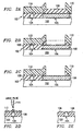
- FIGs 2A - 2D show a fuse etch and probe pad open process according to an embodiment of the invention.
- a semiconductor body 100 is processed though the top metal interconnect 102.
- Semiconductor body 100 is typically a silicon substrate having transistors, isolation structures, and other elements such as capacitors formed therein and/or thereon. Multiple metal interconnect layers are typically formed over the substrate.
- Metal interconnect 102 is the uppermost interconnect layer.
- Metal interconnect 102 comprises a metal, such as aluminum, with appropriate upper and lower barrier layers. Some appropriate barriers include, Ti, TiN, combinations of Ti and TiN, and TaN. In the preferred embodiment, metal interconnect 102 comprises aluminum with an upper barrier layer of TiN.
- Metal interconnect 102 may be used to form a variety of fuses 104 and probe pads 106. Fuses are used to increase yield. For example, in SRAM circuits, after the last interconnect level is formed, the functionality of the device is measured. Probe pads 106 are used to communicate with the device to determine the functionality. Defective interconnect paths are severed by blowing (removing) a fuse. The defective paths are later replaced with alternative interconnect paths.
- fuses An alternative use for fuses is for identifying individual die. Selected fuses are blown, not to eliminate defective paths, but for forming a Die ID. Die Ids are used for tracking and later identifying individual die. These blown fuses are not later replaced with alternative interconnect paths.
- An oxide layer 108 is formed over the top interconnect 102.
- Oxide layer 108 is deposited to a thickness such that the corners of the fuse 104 are just barely covered or just barely exposed.
- the thickness of the oxide 108 above the corners of the fuse is in the range of 0 ⁇ to 1500 ⁇ .
- a thickness of 6000 ⁇ may be used for the oxide layer 108.
- a thicker oxide of approximately 8000 ⁇ was used in the prior art for the same top interconnect height
- an HDP process is used to form oxide layer 108.
- An HDP process has the effect of forming a "top hat” portion over the fuse 106.
- the "top hat” forms as a result of the simultaneous deposition and etch components of an HDP process.
- Using an HDP process has the added advantage of forming material thinner at the corners than over the center of the fuse. The thinner material at the corners provides a known weak point, so the break points during a laser pulse are more predicable.
- Pattern 110 is formed over the oxide layer 108.
- Pattern 110 is typically a photoresist pattern. Pattern 110 covers oxide layer 108 except where probe pads 104 are located. Fuses 106 are covered by pattern 110. This is different from the prior art in which both the probe pads and fuses were exposed.
- pattern 110 the exposed portion of oxide layer 108 over the probe pads 104 is removed, as shown in FIG. 2B.
- an etch chemistry is used that allows for etching of both oxide and TiN.
- the etch clears the oxide 108 and is continued to also remove the upper barrier of top interconnect 102, as shown in FIG. 2C. Suitable etches or combinations of etches are known in the art for etching the oxide and upper barrier layer material. Pattern 110 is then removed.
- the device may be probed to determine functionality using probe pads 106. Defective paths are located and the associated fuses 104 are identified. These associated fuses 104 are the fuses that will be "blown" or removed.
- a conformal oxide layer 112 is deposited over the structure.
- Conformal oxide layer 112 is used to protect the probe pads from the fuse etch process. The fuses that are not going to be removed are also protected by conformal oxide 112. This is important when fuse corners are exposed by oxide 108.
- a thickness of approximately 800 ⁇ to1200 ⁇ may be used for conformal oxide layer 112.
- a plasma enhanced tetraethyoxysilane (PETEOS) process may be used to deposed the conformal oxide layer 112.
- a laser pulse 114 is directed at the fuses 104 to be removed.
- the laser pulse 114 causes cracking at the weakest point.
- the weakest point is typically the upper corners when a HDP process is used to form oxide layer 108. Cracking at the upper corners typically causes the portion of oxide layers 108 and 112 over the fuse 104 to break off as shown in FIG. 2E.
- the prior art processing causes cracking to occur at the lower corners of the fuse through a thicker oxide.
- large cracks could occur that extended to adjacent fuses resulting a loss of the adjacent fuses.
- Only small cracks around the blown fuse sites were found to occur using the process of the invention. Accordingly, the present process may be used with minimum design rule spacings for the fuses without jeopardizing adjacent fuses.
- a wet etch is then used to dissolve the exposed fuses and wash away all debris. Even if the portions of oxide layer 108 and 112 do not break off, sufficient cracks are formed above the fuse to enable the wet etch to dissolve the fuses.
- Suitable wet etch chemistries are known in the art. For example, an etch chemistry of 90sec Surf + 660sec SC1 + 15sec HF may be used.
- Processing then continues to form the alternate interconnect paths, protective overcoat, and packaging.
Landscapes
- Design And Manufacture Of Integrated Circuits (AREA)
Abstract
Description
Claims (12)
- A method for fabricating an integrated circuit comprising:forming a metal interconnect layer over a semiconductor body, said metal interconnect layer comprising a plurality of fuses and a plurality of probe pads;depositing a first oxide layer over the metal interconnect layer, said first oxide layer having a thickness above corners of said plurality of fuses that is less than above centers of said plurality of fuses;conformally depositing a second oxide layer over said first oxide layer and said plurality of probe pads;directing a laser pulse toward a selected subset of said plurality of fuses to form cracks in at least said second oxide layer;wet etching to remove said selected subset of fuses.
- The method of claim 1, wherein depositing said first oxide layer comprises depositing a first oxide layer having a thickness above corners of said plurality of fuses in the range of 0Å to 1500 Å.
- The method of any of claims 1 or claim 2, wherein depositing said first oxide layer comprises depositing a first oxide layer having a thickness of approximately 6000Å at least over said centers of said plurality of fuses.
- The method of claim 3, wherein depositing said first oxide layer comprises depositing said first oxide layer such that corners of the plurality of fuses are exposed.
- The method of any of claims 1-4, wherein depositing said first oxide layer comprises a high density plasma (HDP) oxide deposition such that said first oxide layer is thinner at said corners of each of said fuses than at a center of each of said fuses.
- The method of any of claims 1-5, further comprising:forming a pattern over said first oxide layer, said pattern covering said plurality of fuses and exposing a portion of said first oxide layer over said plurality of probe pads; andremoving said exposed portion of said first oxide layer prior to conformally depositing the second oxide.
- The method of claim 6, wherein removing said exposed portion of said first oxide layer also comprises removing an upper barrier layer of said top interconnect over said probe pads.
- The method of any of claims 1-7, wherein directing a laser pulse comprises directing a laser pulse to thereby cause a portion of said first and second oxide layers over said selected subset of fuses to break off.
- The method of any of claims 1-8, wherein depositing said first oxide layer comprises depositing a first oxide layer to a thickness of approximately the metal layer thickness plus 500 Å.
- The method of any of claims 1-9, wherein depositing said second conformal oxide layer comprises depositing a second conformal oxide layer to a thickness of approximately 800Å to 1200Å.
- The method of any of claims 1-10, further comprising:causing cracks to be formed in said first oxide layer.
- The method of any of claims 1-11, wherein depositing said second oxide layer comprises depositing a second oxide layer having a thickness of approximately 1000Å.
Applications Claiming Priority (2)
| Application Number | Priority Date | Filing Date | Title |
|---|---|---|---|
| US25032400P | 2000-11-30 | 2000-11-30 | |
| US250324 | 2000-11-30 |
Publications (3)
| Publication Number | Publication Date |
|---|---|
| EP1211723A2 true EP1211723A2 (en) | 2002-06-05 |
| EP1211723A3 EP1211723A3 (en) | 2006-04-05 |
| EP1211723B1 EP1211723B1 (en) | 2009-09-09 |
Family
ID=22947265
Family Applications (1)
| Application Number | Title | Priority Date | Filing Date |
|---|---|---|---|
| EP01000649A Expired - Lifetime EP1211723B1 (en) | 2000-11-30 | 2001-11-21 | Optimized metal fuse process in semiconductor device |
Country Status (5)
| Country | Link |
|---|---|
| US (1) | US6687973B2 (en) |
| EP (1) | EP1211723B1 (en) |
| JP (1) | JP4118044B2 (en) |
| AT (1) | ATE442666T1 (en) |
| DE (1) | DE60139850D1 (en) |
Cited By (1)
| Publication number | Priority date | Publication date | Assignee | Title |
|---|---|---|---|---|
| US7799583B2 (en) | 2006-10-02 | 2010-09-21 | Infineon Technologies Ag | System for separation of an electrically conductive connection |
Families Citing this family (6)
| Publication number | Priority date | Publication date | Assignee | Title |
|---|---|---|---|---|
| JP2004055876A (en) * | 2002-07-22 | 2004-02-19 | Renesas Technology Corp | Semiconductor device and method of manufacturing semiconductor device |
| US6835642B2 (en) * | 2002-12-18 | 2004-12-28 | Taiwan Semiconductor Manufacturing Co., Ltd | Method of forming a metal fuse on semiconductor devices |
| JP2004311638A (en) | 2003-04-04 | 2004-11-04 | Renesas Technology Corp | Semiconductor device |
| US20050285222A1 (en) | 2004-06-29 | 2005-12-29 | Kong-Beng Thei | New fuse structure |
| US20100117190A1 (en) * | 2008-11-13 | 2010-05-13 | Harry Chuang | Fuse structure for intergrated circuit devices |
| US10504700B2 (en) | 2015-08-27 | 2019-12-10 | Applied Materials, Inc. | Plasma etching systems and methods with secondary plasma injection |
Family Cites Families (8)
| Publication number | Priority date | Publication date | Assignee | Title |
|---|---|---|---|---|
| JPS57202778A (en) * | 1981-06-08 | 1982-12-11 | Nippon Telegr & Teleph Corp <Ntt> | Substrate for semiconductor integrated circuit and manufacture thereof |
| TW299897U (en) * | 1993-11-05 | 1997-03-01 | Semiconductor Energy Lab | A semiconductor integrated circuit |
| US5521116A (en) * | 1995-04-24 | 1996-05-28 | Texas Instruments Incorporated | Sidewall formation process for a top lead fuse |
| US5747868A (en) * | 1995-06-26 | 1998-05-05 | Alliance Semiconductor Corporation | Laser fusible link structure for semiconductor devices |
| US6100118A (en) * | 1998-06-11 | 2000-08-08 | Taiwan Semiconductor Manufacturing Company, Ltd. | Fabrication of metal fuse design for redundancy technology having a guard ring |
| US6261873B1 (en) * | 1999-04-29 | 2001-07-17 | International Business Machines Corporation | Pedestal fuse |
| US6214681B1 (en) * | 2000-01-26 | 2001-04-10 | Advanced Micro Devices, Inc. | Process for forming polysilicon/germanium thin films without germanium outgassing |
| JP3851752B2 (en) * | 2000-03-27 | 2006-11-29 | 株式会社東芝 | Manufacturing method of semiconductor device |
-
2001
- 2001-11-21 DE DE60139850T patent/DE60139850D1/en not_active Expired - Lifetime
- 2001-11-21 AT AT01000649T patent/ATE442666T1/en not_active IP Right Cessation
- 2001-11-21 EP EP01000649A patent/EP1211723B1/en not_active Expired - Lifetime
- 2001-11-29 JP JP2001364479A patent/JP4118044B2/en not_active Expired - Fee Related
- 2001-11-30 US US09/997,980 patent/US6687973B2/en not_active Expired - Lifetime
Cited By (1)
| Publication number | Priority date | Publication date | Assignee | Title |
|---|---|---|---|---|
| US7799583B2 (en) | 2006-10-02 | 2010-09-21 | Infineon Technologies Ag | System for separation of an electrically conductive connection |
Also Published As
| Publication number | Publication date |
|---|---|
| JP2002203902A (en) | 2002-07-19 |
| DE60139850D1 (en) | 2009-10-22 |
| ATE442666T1 (en) | 2009-09-15 |
| EP1211723B1 (en) | 2009-09-09 |
| US20020062549A1 (en) | 2002-05-30 |
| JP4118044B2 (en) | 2008-07-16 |
| US6687973B2 (en) | 2004-02-10 |
| EP1211723A3 (en) | 2006-04-05 |
Similar Documents
| Publication | Publication Date | Title |
|---|---|---|
| US7977232B2 (en) | Semiconductor wafer including cracking stopper structure and method of forming the same | |
| EP0523856A2 (en) | Method of via formation for multilevel interconnect integrated circuits | |
| JPH0646648B2 (en) | Solid-state circuit with laser fusing link | |
| US6518643B2 (en) | Tri-layer dielectric fuse cap for laser deletion | |
| US6455914B2 (en) | Pedestal fuse | |
| US6355576B1 (en) | Method for cleaning integrated circuit bonding pads | |
| US5066998A (en) | Severable conductive path in an integrated-circuit device | |
| EP1211723B1 (en) | Optimized metal fuse process in semiconductor device | |
| JP2003060036A (en) | Semiconductor device and method of manufacturing the same | |
| US6194318B1 (en) | Manufacturing multiple layered structures of large scale integrated semiconductor devices | |
| US7026233B2 (en) | Method for reducing defects in post passivation interconnect process | |
| US7115512B2 (en) | Methods of forming semiconductor constructions | |
| US6096579A (en) | Method for controlling the thickness of a passivation layer on a semiconductor device | |
| CN105575880B (en) | A kind of production method of semiconductor devices | |
| US7682957B2 (en) | Method of forming pad and fuse in semiconductor device | |
| US20090026585A1 (en) | Semiconductor Device and Method for Manufacturing the same | |
| US7371678B2 (en) | Semiconductor device with a metal line and method of forming the same | |
| JP2766912B2 (en) | Manufacturing method of integrated circuit device | |
| US7022614B2 (en) | Method of etching back of semiconductor wafer | |
| JP2004342922A (en) | Semiconductor device and method of manufacturing semiconductor device | |
| KR100579863B1 (en) | A semiconductor device comprising a method of forming a fuse part on a semiconductor device and a fuse part | |
| JP2006140184A (en) | Semiconductor device manufacturing method and semiconductor device | |
| KR100833588B1 (en) | Manufacturing method of semiconductor device | |
| JP2005101287A (en) | Semiconductor device manufacturing method and semiconductor device | |
| KR19980030827A (en) | Guard ring formation method of semiconductor device |
Legal Events
| Date | Code | Title | Description |
|---|---|---|---|
| PUAI | Public reference made under article 153(3) epc to a published international application that has entered the european phase |
Free format text: ORIGINAL CODE: 0009012 |
|
| AK | Designated contracting states |
Kind code of ref document: A2 Designated state(s): AT BE CH CY DE DK ES FI FR GB GR IE IT LI LU MC NL PT SE TR |
|
| AX | Request for extension of the european patent |
Free format text: AL;LT;LV;MK;RO;SI |
|
| RIN1 | Information on inventor provided before grant (corrected) |
Inventor name: SINGH, ABHA Inventor name: JACKSON, RICKY A. Inventor name: HEWSON, MELISSA M. Inventor name: TRAN, TOAN Inventor name: TIGELAAR, HOWARD |
|
| PUAL | Search report despatched |
Free format text: ORIGINAL CODE: 0009013 |
|
| AK | Designated contracting states |
Kind code of ref document: A3 Designated state(s): AT BE CH CY DE DK ES FI FR GB GR IE IT LI LU MC NL PT SE TR |
|
| AX | Request for extension of the european patent |
Extension state: AL LT LV MK RO SI |
|
| 17P | Request for examination filed |
Effective date: 20061005 |
|
| AKX | Designation fees paid |
Designated state(s): AT BE CH CY DE DK ES FI FR GB GR IE IT LI LU MC NL PT SE TR |
|
| GRAP | Despatch of communication of intention to grant a patent |
Free format text: ORIGINAL CODE: EPIDOSNIGR1 |
|
| GRAS | Grant fee paid |
Free format text: ORIGINAL CODE: EPIDOSNIGR3 |
|
| GRAA | (expected) grant |
Free format text: ORIGINAL CODE: 0009210 |
|
| AK | Designated contracting states |
Kind code of ref document: B1 Designated state(s): AT BE CH CY DE DK ES FI FR GB GR IE IT LI LU MC NL PT SE TR |
|
| REG | Reference to a national code |
Ref country code: GB Ref legal event code: FG4D |
|
| REG | Reference to a national code |
Ref country code: CH Ref legal event code: EP |
|
| REG | Reference to a national code |
Ref country code: IE Ref legal event code: FG4D |
|
| REF | Corresponds to: |
Ref document number: 60139850 Country of ref document: DE Date of ref document: 20091022 Kind code of ref document: P |
|
| PG25 | Lapsed in a contracting state [announced via postgrant information from national office to epo] |
Ref country code: SE Free format text: LAPSE BECAUSE OF FAILURE TO SUBMIT A TRANSLATION OF THE DESCRIPTION OR TO PAY THE FEE WITHIN THE PRESCRIBED TIME-LIMIT Effective date: 20090909 Ref country code: FI Free format text: LAPSE BECAUSE OF FAILURE TO SUBMIT A TRANSLATION OF THE DESCRIPTION OR TO PAY THE FEE WITHIN THE PRESCRIBED TIME-LIMIT Effective date: 20090909 |
|
| PG25 | Lapsed in a contracting state [announced via postgrant information from national office to epo] |
Ref country code: CY Free format text: LAPSE BECAUSE OF FAILURE TO SUBMIT A TRANSLATION OF THE DESCRIPTION OR TO PAY THE FEE WITHIN THE PRESCRIBED TIME-LIMIT Effective date: 20090909 |
|
| PG25 | Lapsed in a contracting state [announced via postgrant information from national office to epo] |
Ref country code: ES Free format text: LAPSE BECAUSE OF FAILURE TO SUBMIT A TRANSLATION OF THE DESCRIPTION OR TO PAY THE FEE WITHIN THE PRESCRIBED TIME-LIMIT Effective date: 20091220 Ref country code: PT Free format text: LAPSE BECAUSE OF FAILURE TO SUBMIT A TRANSLATION OF THE DESCRIPTION OR TO PAY THE FEE WITHIN THE PRESCRIBED TIME-LIMIT Effective date: 20100111 |
|
| PG25 | Lapsed in a contracting state [announced via postgrant information from national office to epo] |
Ref country code: AT Free format text: LAPSE BECAUSE OF FAILURE TO SUBMIT A TRANSLATION OF THE DESCRIPTION OR TO PAY THE FEE WITHIN THE PRESCRIBED TIME-LIMIT Effective date: 20090909 Ref country code: BE Free format text: LAPSE BECAUSE OF FAILURE TO SUBMIT A TRANSLATION OF THE DESCRIPTION OR TO PAY THE FEE WITHIN THE PRESCRIBED TIME-LIMIT Effective date: 20090909 Ref country code: MC Free format text: LAPSE BECAUSE OF NON-PAYMENT OF DUE FEES Effective date: 20091130 |
|
| REG | Reference to a national code |
Ref country code: CH Ref legal event code: PL |
|
| PLBE | No opposition filed within time limit |
Free format text: ORIGINAL CODE: 0009261 |
|
| STAA | Information on the status of an ep patent application or granted ep patent |
Free format text: STATUS: NO OPPOSITION FILED WITHIN TIME LIMIT |
|
| PG25 | Lapsed in a contracting state [announced via postgrant information from national office to epo] |
Ref country code: DK Free format text: LAPSE BECAUSE OF FAILURE TO SUBMIT A TRANSLATION OF THE DESCRIPTION OR TO PAY THE FEE WITHIN THE PRESCRIBED TIME-LIMIT Effective date: 20090909 |
|
| 26N | No opposition filed |
Effective date: 20100610 |
|
| PG25 | Lapsed in a contracting state [announced via postgrant information from national office to epo] |
Ref country code: LI Free format text: LAPSE BECAUSE OF NON-PAYMENT OF DUE FEES Effective date: 20091130 Ref country code: GR Free format text: LAPSE BECAUSE OF FAILURE TO SUBMIT A TRANSLATION OF THE DESCRIPTION OR TO PAY THE FEE WITHIN THE PRESCRIBED TIME-LIMIT Effective date: 20091210 Ref country code: CH Free format text: LAPSE BECAUSE OF NON-PAYMENT OF DUE FEES Effective date: 20091130 Ref country code: IE Free format text: LAPSE BECAUSE OF NON-PAYMENT OF DUE FEES Effective date: 20091121 |
|
| PG25 | Lapsed in a contracting state [announced via postgrant information from national office to epo] |
Ref country code: IT Free format text: LAPSE BECAUSE OF FAILURE TO SUBMIT A TRANSLATION OF THE DESCRIPTION OR TO PAY THE FEE WITHIN THE PRESCRIBED TIME-LIMIT Effective date: 20090909 |
|
| PG25 | Lapsed in a contracting state [announced via postgrant information from national office to epo] |
Ref country code: LU Free format text: LAPSE BECAUSE OF NON-PAYMENT OF DUE FEES Effective date: 20091121 |
|
| PG25 | Lapsed in a contracting state [announced via postgrant information from national office to epo] |
Ref country code: TR Free format text: LAPSE BECAUSE OF FAILURE TO SUBMIT A TRANSLATION OF THE DESCRIPTION OR TO PAY THE FEE WITHIN THE PRESCRIBED TIME-LIMIT Effective date: 20090909 |
|
| REG | Reference to a national code |
Ref country code: FR Ref legal event code: PLFP Year of fee payment: 15 |
|
| REG | Reference to a national code |
Ref country code: FR Ref legal event code: PLFP Year of fee payment: 16 |
|
| PGFP | Annual fee paid to national office [announced via postgrant information from national office to epo] |
Ref country code: DE Payment date: 20161130 Year of fee payment: 16 Ref country code: GB Payment date: 20161026 Year of fee payment: 16 Ref country code: FR Payment date: 20161017 Year of fee payment: 16 Ref country code: NL Payment date: 20161107 Year of fee payment: 16 |
|
| REG | Reference to a national code |
Ref country code: DE Ref legal event code: R119 Ref document number: 60139850 Country of ref document: DE |
|
| REG | Reference to a national code |
Ref country code: NL Ref legal event code: MM Effective date: 20171201 |
|
| GBPC | Gb: european patent ceased through non-payment of renewal fee |
Effective date: 20171121 |
|
| REG | Reference to a national code |
Ref country code: FR Ref legal event code: ST Effective date: 20180731 |
|
| PG25 | Lapsed in a contracting state [announced via postgrant information from national office to epo] |
Ref country code: DE Free format text: LAPSE BECAUSE OF NON-PAYMENT OF DUE FEES Effective date: 20180602 Ref country code: NL Free format text: LAPSE BECAUSE OF NON-PAYMENT OF DUE FEES Effective date: 20171201 Ref country code: FR Free format text: LAPSE BECAUSE OF NON-PAYMENT OF DUE FEES Effective date: 20171130 |
|
| PG25 | Lapsed in a contracting state [announced via postgrant information from national office to epo] |
Ref country code: GB Free format text: LAPSE BECAUSE OF NON-PAYMENT OF DUE FEES Effective date: 20171121 |