EP1209730A2 - High temperature electrode and barrier structure for FRAM and DRAM applications - Google Patents
High temperature electrode and barrier structure for FRAM and DRAM applications Download PDFInfo
- Publication number
- EP1209730A2 EP1209730A2 EP01309533A EP01309533A EP1209730A2 EP 1209730 A2 EP1209730 A2 EP 1209730A2 EP 01309533 A EP01309533 A EP 01309533A EP 01309533 A EP01309533 A EP 01309533A EP 1209730 A2 EP1209730 A2 EP 1209730A2
- Authority
- EP
- European Patent Office
- Prior art keywords
- layer
- ruo
- electrode
- depositing
- group
- Prior art date
- Legal status (The legal status is an assumption and is not a legal conclusion. Google has not performed a legal analysis and makes no representation as to the accuracy of the status listed.)
- Withdrawn
Links
Images


Classifications
-
- H—ELECTRICITY
- H10—SEMICONDUCTOR DEVICES; ELECTRIC SOLID-STATE DEVICES NOT OTHERWISE PROVIDED FOR
- H10D—INORGANIC ELECTRIC SEMICONDUCTOR DEVICES
- H10D64/00—Electrodes of devices having potential barriers
- H10D64/01—Manufacture or treatment
- H10D64/013—Manufacture or treatment of electrodes having a conductor capacitively coupled to a semiconductor by an insulator
- H10D64/01302—Manufacture or treatment of electrodes having a conductor capacitively coupled to a semiconductor by an insulator the insulator being formed after the semiconductor body, the semiconductor being silicon
- H10D64/01304—Manufacture or treatment of electrodes having a conductor capacitively coupled to a semiconductor by an insulator the insulator being formed after the semiconductor body, the semiconductor being silicon characterised by the conductor
- H10D64/01318—Manufacture or treatment of electrodes having a conductor capacitively coupled to a semiconductor by an insulator the insulator being formed after the semiconductor body, the semiconductor being silicon characterised by the conductor the conductor comprising a layer of alloy material, compound material or organic material contacting the insulator, e.g. TiN
-
- H—ELECTRICITY
- H10—SEMICONDUCTOR DEVICES; ELECTRIC SOLID-STATE DEVICES NOT OTHERWISE PROVIDED FOR
- H10P—GENERIC PROCESSES OR APPARATUS FOR THE MANUFACTURE OR TREATMENT OF DEVICES COVERED BY CLASS H10
- H10P14/00—Formation of materials, e.g. in the shape of layers or pillars
- H10P14/40—Formation of materials, e.g. in the shape of layers or pillars of conductive or resistive materials
-
- H—ELECTRICITY
- H10—SEMICONDUCTOR DEVICES; ELECTRIC SOLID-STATE DEVICES NOT OTHERWISE PROVIDED FOR
- H10D—INORGANIC ELECTRIC SEMICONDUCTOR DEVICES
- H10D64/00—Electrodes of devices having potential barriers
- H10D64/01—Manufacture or treatment
- H10D64/013—Manufacture or treatment of electrodes having a conductor capacitively coupled to a semiconductor by an insulator
- H10D64/01302—Manufacture or treatment of electrodes having a conductor capacitively coupled to a semiconductor by an insulator the insulator being formed after the semiconductor body, the semiconductor being silicon
- H10D64/01332—Making the insulator
- H10D64/01336—Making the insulator on single crystalline silicon, e.g. chemical oxidation using a liquid
- H10D64/01338—Making the insulator on single crystalline silicon, e.g. chemical oxidation using a liquid with a treatment, e.g. annealing, after the formation of the conductor
-
- H—ELECTRICITY
- H10—SEMICONDUCTOR DEVICES; ELECTRIC SOLID-STATE DEVICES NOT OTHERWISE PROVIDED FOR
- H10D—INORGANIC ELECTRIC SEMICONDUCTOR DEVICES
- H10D64/00—Electrodes of devices having potential barriers
- H10D64/01—Manufacture or treatment
- H10D64/031—Manufacture or treatment of data-storage electrodes
- H10D64/033—Manufacture or treatment of data-storage electrodes comprising ferroelectric layers
-
- H—ELECTRICITY
- H10—SEMICONDUCTOR DEVICES; ELECTRIC SOLID-STATE DEVICES NOT OTHERWISE PROVIDED FOR
- H10D—INORGANIC ELECTRIC SEMICONDUCTOR DEVICES
- H10D64/00—Electrodes of devices having potential barriers
- H10D64/60—Electrodes characterised by their materials
- H10D64/66—Electrodes having a conductor capacitively coupled to a semiconductor by an insulator, e.g. MIS electrodes
- H10D64/667—Electrodes having a conductor capacitively coupled to a semiconductor by an insulator, e.g. MIS electrodes the conductor comprising a layer of alloy material, compound material or organic material contacting the insulator, e.g. TiN workfunction layers
-
- H—ELECTRICITY
- H10—SEMICONDUCTOR DEVICES; ELECTRIC SOLID-STATE DEVICES NOT OTHERWISE PROVIDED FOR
- H10B—ELECTRONIC MEMORY DEVICES
- H10B12/00—Dynamic random access memory [DRAM] devices
- H10B12/01—Manufacture or treatment
- H10B12/02—Manufacture or treatment for one transistor one-capacitor [1T-1C] memory cells
- H10B12/05—Making the transistor
Definitions
- This invention relates to FeRAM and DRAM semiconductors, and specifically to the use of barrier layers and electrodes which remain stable during and after high-temperature annealing.
- FeRAM and DRAM semiconductors are susceptible to breakdown of intermediate layers during manufacturing, and particularly during high-temperature annealing steps which must occur to diffuse implanted ions within active regions. Further, when completed, semiconductors are subjected to high-temperature environments, such as in the aerospace industry, FeRAM and DRAM semiconductors constructed by conventional methods may fail. Previous work in this field has been conducted and reported in the following publications:
- a semiconductor structure includes a substrate taken from the group of substrates consisting of silicon, polysilicon, silicon dioxide and silicon germanium; and an electrode, located above the substrate, which includes a layer of composition Ir-M-O, wherein M is taken from the group of metals consisting of Ta, Ti, Nb, Al, Hf, Zr and V; wherein the semiconductor structure is constructed and arranged to withstand annealing at a temperature greater than or equal to 600°C without losing conductivity and integrity:
- a method of forming a semiconductor structure includes preparing a substrate taken from the group of substrates consisting of silicon, polysilicon, silicon dioxide and silicon germanium; depositing successive layers of materials including depositing an electrode layer of composition Ir-M-O, wherein M is taken from the group of metals consisting of Ta, Ti, Nb, Al,Hf, Zr and V; and annealing the semiconductor structure at a temperature greater than or equal to 600°C.
- An object of the invention is to provide a bottom electrode or barrier structure on a substrate in a non-volatile memory application wherein the structure can tolerate high-temperature annealing, i . e ., above 600°C, without losing conductivity and integrity.
- Another object of the invention is to provide a Ir-M-O layer as an electrode or barrier structure, where M is a metal.
- Another object of the invention is to prevent oxidation of a Ta barrier layer by providing a thin metal layer as a second barrier layer between a layer comprised of Ir-Ta-O and a layer of Ta.
- a further object of the invention is to prevent oxidation of an Ir-Ta-O electrode by depositing a layer containing Ir, IrO 2 , Pt, Ru, or RuO 2 on top of a Ir-Ta-O electrode
- Yet another object of the invention is to provide an Ir-Ta-O layer on a substrate taken from the group of substrates consisting of Si, SiO 2 , SiGe and polysilicon.
- Iridium-Metal-Oxygen/Metal (Ir-M-O/M) layer as a bottom electrode or barrier structure in non-volatile memory applications has the advantage of being able to withstand temperatures above 600°C, up to 1000°C, without losing its conductivity or integrity, where the metal is taken from the group of metals including tantalum (Ta), titanium (Ti), niobium (Nb), hafnium (Hf), aluminum (Al), zirconium (Zr) and vanadium (V). Further, such a structure is capable of withstanding high operating temperatures once the semiconductor is completed and installed in a real-world system.
- the oxidation of a M barrier layer may be prevented by inserting a thin M* barrier layer between an Ir-M-O layer and a M layer, e . g ., M may be Ta and M* may be Ir.
- An Ir-M-O/MO layer where MO represents the metal oxides, including Ta 2 O 5 , TiO 2 , Nb 2 O 5 , HfO 2 , Al 2 O 3 , ZrO 2 and V 2 O 5 , is suitable as a bottom electrode for metal-ferro-insulator-silicon (MFIS) applications.
- Oxidation of an Ir-M-O electrode may be prevented by depositing a metal layer, such as Ir, IrO 2 , Ru, or RuO 2 , on top of an Ir-M-O electrode.
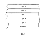
- the embodiments of the invention include multi-layer structures which are formed on a substrate layer, wherein the substrate may be silicon, polysilicon or silicon-germanium.
- a MOS structure may be formed on a silicon oxide substrate.
- the structure includes at least one barrier layer located between the substrate and a Ir-M-O electrode.
- a first, or bottom, barrier layer, Layer A is formed on the substrate.
- Layer A may include Ti or TiN, and provides a conductive layer between the substrate and electrode.
- a second barrier layer, Layer B is an optional layer, and may include Ta, TaN, TaSiN, Nb, NbN, AlN, Al-Ti, Al-Ti-N, Hf, HfN, Zr, ZrN, V or VN.
- the first and the second barrier layers may be deposited on the substrate by CVD, PVD, MOCVD or other thin film deposition methods.
- Layer A including Ti
- the second barrier layer may be deposited by DC sputtering in pure Ar, or by any other state of the art deposition technique, at a temperature of between room temperature and about 600°C.
- the second barrier layer may be deposited by DC sputtering in pure Ar when using Ta, Nb, Zr, Hf or Al-Ti as the metal, or, the second barrier layer may be deposited by reactive sputtering in an Ar-N 2 atmosphere at ambient temperature when using TaN, TaSiN, NbN, AIN, HfN, ZrN or VN as the metal.
- the total thickness of the first and second barrier layer is preferably between about 10nm and 200nm.
- a third, or middle, barrier layer, Layer C may include Ir, IrO 2 , Pt, Ru or RuO 2 , or may be formed as a double layer structure of IrO 2 /Ir, IrO 2 /Pt, RuO 2 /Ir, RuO 2 /Pt or RuO 2 /Ru, having an arrangement of a metal layer on top of a metal oxide layer, or a metal oxide layer on top of a metal layer, on Layer B.
- Layer C may be deposited by PVD or CVD, MOCVD or other thin film deposition method, and has a thickness of between about 10nm to 300nm.
- An electrode layer, Layer D has the composition Ir-M-O, where M is a metal from the group including Ta, Ti, Nb, Al, Hf, Zr and V, and is formed on the uppermost of barrier Layers A, B or C.
- Layer D may be formed by PVD, CVD, MOCVD or other thin film deposition methods. The thickness of Layer D is between about 10nm to 500nm.
- Electrode layer D may be formed by co-sputtering Ir and the metal target at 300W, for four inch diameter targets, on each target at a chamber pressure of about 10mTorr., in an Ar/O 2 flow having a rate of 1:1.
- An optional fourth,'or top, barrier layer, Layer E may include Ir, IrO 2 , ruthenium (Ru), RuO 2 , or platinum (Pt), or may be formed as a double layer structure of IrO 2 /Ir, IrO 2 /Pt, RuO 2 /Ir, RuO 2 /Pt or RuO 2 /Ru, with the metal layer either above or below the metal oxide layer, on electrode Layer D.
- Layer E is formed of a low resistivity metal or metal oxide, and may be deposited by PVD, CVD, MOCVD or other thin film deposition methods, with a thickness of between about 10nm to 200nm.
- a post deposition annealing in an O 2 ambient atmosphere is done at a temperature in a range of between about 600°C and 900°C to stabilize the structure.
- the structures described herein may be used as conductive bottom electrode and/or barrier structures on silicon, polysilicon, and silicon germanium substrates in nonvolatile memories, such as MFMS, MFMOS, MFIS, MIFS, and MFS memories, DRAM, capacitors, pyroelectric infrared sensors, optical displays, optical switches, piezoelectric transducers and surface acoustic wave devices.
- nonvolatile memories such as MFMS, MFMOS, MFIS, MIFS, and MFS memories, DRAM, capacitors, pyroelectric infrared sensors, optical displays, optical switches, piezoelectric transducers and surface acoustic wave devices.
- the structures may be formed on silicon oxide substrates to form MOS type devices, such as MFMOS devices.
- the conductivity of the electrode layers may be varied by changing the relative metal composition ratio.
- an annealing step in an O 2 atmosphere is necessary to lower the resistance of the Ir-M-O film, and to stabilize the structure's thickness.
- This annealing step may also be performed by annealing in other atmospheres, such as N 2 , Ar, or in a vacuum, at temperatures above 600 ° C.
- the as-deposited Ir-Ta-O Layer D may obtain its lowest resistance by post deposition annealing at 800°C to 900°C in O 2 ambient for between about one to thirty minutes.
- the thickness of the structure can be stabilized by annealing at a temperature above 600°C.
- the second embodiment of the invention uses only four layers, wherein Layers A and B are not used, and includes structures which have an Ir-M-O electrode layer, Layer D, where M is again taken from the group of metals consisting of Ta, Ti, Nb, Al, Hf, Zr and V, and which may be formed without a barrier layer directly on a silicon, polysilicon or silicon-germanium substrate, by CVD, PVD, MOCVD, or any other thin film deposition technique.
- Layer D has a thickness of between about 10nm and 500nm, when used in FeRAM and DRAM applications.
- the structure may be formed on a silicon oxide substrate to form a MOS structure.
- Ir-M-O bottom electrode Because a low contact resistance is required between an Ir-M-O bottom electrode and silicon or polysilicon substrates, it is necessary to provide a structure which can maintain low contact resistance during high temperature ambient oxygen annealing processes.
- the use of an Ir-M-O layer as an electrode on Si, polysilicon and SiGe substrates for FeRAM and DRAM applications provides such a low contact resistance.
- An optional barrier layer, Layer C may include an Ir, IrO 2 , Ru, RuO 2 , or Pt layer; or may be formed as a double layer structure of IrO 2 /Ir, IrO 2 /Pt, RuO 2 /Ir, RuO 2 /Pt or RuO 2 /Ru, with the metal layer either above or below the metal oxide layer, and may be deposited on the substrate first before electrode Layer D.
- Layer C has a preferable thickness of between about 10nm to 300nm, and may be deposited by PVD, CVD, MOCVD, or any other thin film deposition method.
- An optional top barrier layer, Layer E may include Ir, IrO 2 , Pt, Ru or RuO 2 , or may be formed as a double layer structure of IrO 2 /Ir, IrO 2 /Pt, RuO 2 /Ir, RuO 2 /Pt or RuO 2 /Ru, with the metal either above or below the metal oxide, and may be deposited on top of the electrode, having a total thickness of between about 10nm to 300nm.
- the top barrier layer may be deposited by PVD or CVD, MOCVD or other thin film deposition methods.
- the function of barrier Layer E is to prevent the oxygen diffusion to the substrate. This structure may be used in capacitors, sensors, displays and transducer applications.
- the conductivity of the Ir-M-O electrode layers may be varied by changing the relative composition ratio of metal.
- Post annealing in O 2 is provided to lower the sheet resistivity and to stabilize the thickness of the structure.
- Post annealing may be performed by annealing in other gases, such as N 2 , Ar, or in a vacuum, at temperatures above 600 ° C.
- an as-deposited Ir-Ta-O layer obtains its lowest resistance by post deposition annealing at 800°C to 900°C in an O 2 ambient atmosphere for one to thirty minutes.
- MOS 10 is constructed by directly depositing Ir-Ta-O electrodes on a gate oxide layer having thickness of 20 ⁇ or 35 ⁇ .
- An electrode layer of Ir-Ta-O was formed by cosputtering Ir and Ta four-inch diameter targets at 300W with a chamber pressure of 10 mTorr. in a Ar/O 2 atmosphere at a flow rate ratio of 1:1.
- a post deposition annealing in O 2 ambient was done at 800°C for ten minutes in order to characterize the thermal stability of these structures.
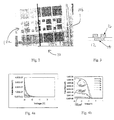
- Fig. 2 depicts the Ir-Ta-O/gate oxide/Si structure 10 before (10a) and after (10b) O 2 ambient annealing at 800°C for ten minutes. It can be seen from Fig. 2 that the Ir-Ta-O/gate oxide/Si structure is very stable even after the high-temperature anneal. Hillock and/or peeling were not observed. However, the as-deposited Ir-Ta-O/gate oxide/Si structures with 20 ⁇ and 35 ⁇ gate oxides were both very leaky. After 800°C oxygen ambient annealing for ten minutes, good C-V characteristics were obtained as shown in Figs. 4b and 6b. The leakage current was significantly reduced. This is due to the interface between Ir-Ta-O and gate oxide was further oxidized during oxygen ambient annealing. The equivalent oxide thickness after annealing is around 40 ⁇ to 50 ⁇ .
- Fig. 3 is a cross-section of MOS structure 10 of Fig. 2, depicting substrate 12, a gate oxide layer 14 and an Ir-Ta-O electrode layer 16.
- Fig. 4a depicts the C-V of as-deposited Ir-Ta-O/gate oxide/Si structure of three sizes of capacitors: 400 ⁇ m 2 , 200 ⁇ m 2 and 100 ⁇ m 2 , having a 20 ⁇ gate oxide;
- Fig. 4b depicts the C-V of the three structures after annealing at 800°C in O 2 for ten minutes (dashed lines), then annealing in Forming gas at 450°C for fifteen minutes (solid lines).
- Fig. 5a depicts the I-V of as-deposited Ir-Ta-O/gate oxide/Si structure of a 100 ⁇ m 2 capacitor having a 20 ⁇ gate oxide
- Fig. 5b depicts the I-V of the structure after annealing at 800°C in O 2 for ten minutes, then annealing in Forming gas at 450°C for fifteen minutes
- Fig. 6a depicts the C-V of as-deposited Ir-Ta-O/gate oxide/Si structure of three sizes of capacitors: 400 ⁇ m 2 , 200 ⁇ m 2 and 100 ⁇ m 2 , having a 35 ⁇ gate oxide
- Fig. 6b depicts the C-V of the three structures after annealing at 800°C in O 2 for ten minutes (dashed lines), then annealing in Forming gas at 450°C for fifteen minutes (solid lines).
- Fig. 7a depicts the I-V of as-deposited Ir-Ta-O/gate oxide/Si structure of a 100 ⁇ m 2 capacitor having a 35 ⁇ gate oxide
- Fig. 7b depicts the I-V of the structure after annealing at 800°C in O 2 for ten minutes; then annealing in Forming gas at 450°C for fifteen minutes.
- the C-V characteristics of Figs. 4 and 6 include three sizes of capacitors at: 400 ⁇ m 2 , 200 ⁇ m 2 and 100 ⁇ m 2 .
- the I-V characteristics of Figs 5 and 7 only include 100 ⁇ m 2 capacitors.
- the first barrier layer or the second barrier layer, or both may be applied if further oxidation between a Ir-Ta-O layer and gate oxide layer needs to be minimized. Good contact resistance may be maintained for the Ir-Ta-O/silicon, polysilicon, or silicon germanium structure if the first barrier layer, or the second barrier layer, or both, are used.
- the first barrier layer and the second barrier layer is a layer of Ir, IrO 2 , Ru, RuO 2 and Pt, or a double layer of IrO 2 /Ir , IrO 2 /Pt, RuO 2 /Ir, RuO 2 /Pt or RuO 2 /Ru, with a metal layer on top of or under a metal oxide layer.
Landscapes
- Semiconductor Memories (AREA)
- Electrodes Of Semiconductors (AREA)
Abstract
Description
The steps in the formation process may be summarized as follows:
Fig. 6a depicts the C-V of as-deposited Ir-Ta-O/gate oxide/Si structure of three sizes of capacitors: 400 µm2, 200µm2 and 100µm2, having a 35Å gate oxide; Fig. 6b depicts the C-V of the three structures after annealing at 800°C in O2 for ten minutes (dashed lines), then annealing in Forming gas at 450°C for fifteen minutes (solid lines).
Claims (21)
- A semiconductor structure comprising:a substrate taken from the group of substrates consisting of silicon, polysilicon, silicon dioxide and silicon germanium; andan electrode, located above said substrate, which includes a layer of composition Ir-M-O, wherein M is take from the group of metals consisting of Ta, Ti, Nb, Al, Hf, Zr and V;wherein the semiconductor structure is constructed and arranged to withstand annealing at a temperature greater than or equal to 600 °C without losing conductivity and integrity.
- The semiconductor structure of claim 1 which further includes a bottom barrier layer located between said electrode and said substrate, including a layer of material taken from the group of materials consisting of Ti and TiN.
- The semiconductor structure of claim 1 which further includes a second barrier layer formed between said electrode and said substrate, including a layer of material taken from the group of materials consisting of Ta, TaN, TaSiN, Nb, NbN, AlN, Zr, ZrN, Hf, HfN, Al-Ti and Al-Ti-N.
- The semiconductor structure of claim 1 which further includes a third barrier layer formed between said electrode and said substrate, including a layer of material taken from the group of materials consisting of IrO2/Ir, IrO2/Pt, RuO2/Ir, RuO2/Pt and RuO2/Ru, wherein the third barrier layer comprises a metal oxide layer formed on a metal layer.
- The semiconductor structure of claim 1 which further includes a third barrier layer formed between said electrode and said substrate, including a layer of material taken from the group of materials consisting of IrO2/Ir, IrO2/Pt, RuO2/Ir, RuO2/Pt and RuO2/Ru, wherein the third barrier layer comprises a metal layer formed on a metal oxide layer.
- The semiconductor structure of claim 1 which further includes a third barrier layer formed between said electrode and said substrate, including a layer of material taken from the group of materials consisting of Ir, IrO2, Pt, Ru and RuO2.
- The semiconductor structure of claim 1 which further includes a top barrier layer formed above said electrode, including a layer of material taken from the group of materials consisting of IrO2/Ir, IrO2/Pt, RuO2/Ir, RuO2/Pt and RuO2/Ru, wherein the top barrier layer comprises a metal oxide layer formed on a metal layer.
- The semiconductor structure of claim 1 which further includes a top barrier layer formed above said electrode, including a layer of material taken from the group of materials consisting of IrO2/Ir, IrO2/Pt, RuO2/Ir, RuO2/Pt and RuO2/Ru, wherein the top barrier layer comprises a metal layer formed on a metal oxide layer.
- The semiconductor structure of claim 1 which further includes a top barrier layer formed above said electrode, including a layer of material taken from the group of materials consisting of Ir, IrO2, Pt, Ru and RuO2.
- The semiconductor structure of claim 1 which includes a layer of oxide located between said electrode and said substrate.
- The semiconductor structure of claim 1 which includes a conductive layer located between said electrode and said substrate.
- A method of forming a semiconductor structure comprising:preparing a substrate taken from the group of substrates consisting of silicon, polysilicon, silicon dioxide and silicon germanium;depositing successive layers of materials including depositing an electrode layer of composition Ir-M-O, wherein M is taken from the group of metals consisting of Ta, Ti, Nb, Hf, Zr and V; andannealing the semiconductor structure at a temperature greater than or equal to 600°C.
- The method claim 12 wherein said depositing includes depositing a first barrier layer of materials taken from the group of materials consisting of Ti and TiN.
- The method of claim 13 wherein said depositing further includes depositing a second barrier layer between the substrate and the electrode including a layer of material taken from the group of materials consisting of Ta, TaN, TaSiN, Nb, NbN, AlN, Zr, ZrN, Hf, HfN, Al-Ti and Al-Ti-N.
- The method of claim 14 wherein said depositing includes depositing the first barrier layer and the second barrier layer to a combined thickness in a range of between about 10nm to 200nm.
- The method of claim 12 wherein said depositing further includes depositing a third barrier layer below the electrode, including depositing a layer of material taken from the group of materials consisting of IrO2/Ir, IrO2/Pt, RuO2/Ir, RuO2/Pt and RuO2/Ru, wherein the third barrier layer has an arrangement taken from the group of arrangements consisting of forming a metal oxide layer on a metal layer and forming a metal layer on a metal oxide layer.
- The method of claim 12 wherein said depositing further includes depositing a third barrier layer below the electrode, including depositing a layer of material taken from the group of materials consisting of Ir, IrO2, Pt, Ru and RuO.
- The method of claim 12 wherein said depositing further includes depositing a top barrier layer above the electrode, including depositing a layer of material taken from the group of materials consisting of IrO2/Ir, IrO2/Pt, RuO2/Ir, RuO2/Pt and RuO2/Ru, wherein the top barrier layer has an arrangement taken from the group of arrangements consisting of forming a metal oxide layer on a metal layer and forming a metal layer on a metal oxide layer.
- The method of claim 12 wherein said depositing further includes depositing a top barrier layer above the electrode, including depositing a layer of material taken from the group of materials consisting of Ir, IrO2, Pt, Ru and RuO.
- The method of claim 10 wherein said depositing includes depositing an electrode layer and simultaneously forming an oxide layer between the electrode and the substrate.
- The method of claim 10 wherein said depositing includes depositing a conductive layer on said substrate.
Applications Claiming Priority (2)
| Application Number | Priority Date | Filing Date | Title |
|---|---|---|---|
| US72180000A | 2000-11-22 | 2000-11-22 | |
| US721800 | 2000-11-22 |
Publications (2)
| Publication Number | Publication Date |
|---|---|
| EP1209730A2 true EP1209730A2 (en) | 2002-05-29 |
| EP1209730A3 EP1209730A3 (en) | 2004-05-19 |
Family
ID=24899347
Family Applications (1)
| Application Number | Title | Priority Date | Filing Date |
|---|---|---|---|
| EP01309533A Withdrawn EP1209730A3 (en) | 2000-11-22 | 2001-11-12 | High temperature electrode and barrier structure for FRAM and DRAM applications |
Country Status (4)
| Country | Link |
|---|---|
| EP (1) | EP1209730A3 (en) |
| JP (1) | JP2002198324A (en) |
| KR (1) | KR100437071B1 (en) |
| TW (1) | TW518748B (en) |
Cited By (1)
| Publication number | Priority date | Publication date | Assignee | Title |
|---|---|---|---|---|
| WO2020210263A1 (en) * | 2019-04-08 | 2020-10-15 | Kepler Computing Inc. | Doped polar layers and semiconductor device incorporating same |
Families Citing this family (1)
| Publication number | Priority date | Publication date | Assignee | Title |
|---|---|---|---|---|
| KR102247015B1 (en) | 2014-10-14 | 2021-05-03 | 삼성전자주식회사 | Semiconductor device including a capacitor and method of fabricating the same |
Citations (1)
| Publication number | Priority date | Publication date | Assignee | Title |
|---|---|---|---|---|
| EP1054440A2 (en) * | 1999-05-21 | 2000-11-22 | Sharp Kabushiki Kaisha | Composite iridium barrier structure with oxidized refractory metal companion barrier and method for its fabrication |
Family Cites Families (4)
| Publication number | Priority date | Publication date | Assignee | Title |
|---|---|---|---|---|
| JP3454058B2 (en) * | 1996-12-11 | 2003-10-06 | 富士通株式会社 | Semiconductor memory and manufacturing method thereof |
| US6011284A (en) * | 1996-12-26 | 2000-01-04 | Sony Corporation | Electronic material, its manufacturing method, dielectric capacitor, nonvolatile memory and semiconductor device |
| JP2000223666A (en) * | 1999-01-28 | 2000-08-11 | Sharp Corp | Method for manufacturing semiconductor memory device |
| US6236113B1 (en) * | 1999-03-05 | 2001-05-22 | Sharp Laboratories Of America, Inc. | Iridium composite barrier structure and method for same |
-
2001
- 2001-11-05 JP JP2001339963A patent/JP2002198324A/en active Pending
- 2001-11-09 TW TW090127883A patent/TW518748B/en not_active IP Right Cessation
- 2001-11-12 EP EP01309533A patent/EP1209730A3/en not_active Withdrawn
- 2001-11-15 KR KR10-2001-0071075A patent/KR100437071B1/en not_active Expired - Fee Related
Patent Citations (1)
| Publication number | Priority date | Publication date | Assignee | Title |
|---|---|---|---|---|
| EP1054440A2 (en) * | 1999-05-21 | 2000-11-22 | Sharp Kabushiki Kaisha | Composite iridium barrier structure with oxidized refractory metal companion barrier and method for its fabrication |
Cited By (24)
| Publication number | Priority date | Publication date | Assignee | Title |
|---|---|---|---|---|
| WO2020210263A1 (en) * | 2019-04-08 | 2020-10-15 | Kepler Computing Inc. | Doped polar layers and semiconductor device incorporating same |
| US11164976B2 (en) | 2019-04-08 | 2021-11-02 | Kepler Computing Inc. | Doped polar layers and semiconductor device incorporating same |
| US11289608B2 (en) | 2019-04-08 | 2022-03-29 | Kepler Computing Inc. | Doped polar layers and semiconductor device incorporating same |
| US11289607B2 (en) | 2019-04-08 | 2022-03-29 | Kepler Computing Inc. | Doped polar layers and semiconductor device incorporating same |
| US11296228B2 (en) | 2019-04-08 | 2022-04-05 | Kepler Computing Inc. | Doped polar layers and semiconductor device incorporating same |
| US11349031B2 (en) | 2019-04-08 | 2022-05-31 | Kepler Computing Inc. | Doped polar layers and semiconductor device incorporating same |
| US11355643B2 (en) | 2019-04-08 | 2022-06-07 | Kepler Computing Inc. | Doped polar layers and semiconductor device incorporating same |
| US11398570B2 (en) | 2019-04-08 | 2022-07-26 | Kepler Computing Inc. | Doped polar layers and semiconductor device incorporating same |
| US11411116B2 (en) | 2019-04-08 | 2022-08-09 | Kepler Computing Inc. | Doped polar layers and semiconductor device incorporating same |
| US11417768B2 (en) | 2019-04-08 | 2022-08-16 | Kepler Computing Inc. | Doped polar layers and semiconductor device incorporating same |
| US11444203B2 (en) | 2019-04-08 | 2022-09-13 | Kepler Computing Inc. | Doped polar layers and semiconductor device incorporating same |
| US11469327B2 (en) | 2019-04-08 | 2022-10-11 | Kepler Computing Inc. | Doped polar layers and semiconductor device incorporating same |
| US11757043B2 (en) | 2019-04-08 | 2023-09-12 | Kepler Computing Inc. | Doped polar layers and semiconductor device incorporating same |
| US11837664B2 (en) | 2019-04-08 | 2023-12-05 | Kepler Computing Inc. | Doped polar layers and semiconductor device incorporating same |
| US11848386B2 (en) | 2019-04-08 | 2023-12-19 | Kepler Computing Inc. | B-site doped perovskite layers and semiconductor device incorporating same |
| US11888067B2 (en) | 2019-04-08 | 2024-01-30 | Kepler Computing Inc. | B-site doped perovskite layers and semiconductor device incorporating same |
| US11888066B2 (en) | 2019-04-08 | 2024-01-30 | Kepler Computing Inc. | Doped polar layers and semiconductor device incorporating same |
| US11908943B2 (en) | 2019-04-08 | 2024-02-20 | Kepler Computing Inc. | Manganese-doped perovskite layers and semiconductor device incorporating same |
| US11916149B2 (en) | 2019-04-08 | 2024-02-27 | Kepler Computing Inc. | Doped polar layers and semiconductor device incorporating same |
| US11949017B2 (en) | 2019-04-08 | 2024-04-02 | Kepler Computing Inc. | Doped polar layers and semiconductor device incorporating same |
| US11949018B2 (en) | 2019-04-08 | 2024-04-02 | Kepler Computing Inc. | Doped polar layers and semiconductor device incorporating same |
| US12294029B2 (en) | 2019-04-08 | 2025-05-06 | Kepler Computing Inc. | Doped polar layers and semiconductor device incorporating same |
| US12369351B2 (en) | 2019-04-08 | 2025-07-22 | Kepler Computing Inc. | Doped polar layers and semiconductor device incorporating same |
| US12501656B2 (en) | 2019-04-08 | 2025-12-16 | Kepler Computing Inc. | Doped polar layers and semiconductor device incorporating same |
Also Published As
| Publication number | Publication date |
|---|---|
| TW518748B (en) | 2003-01-21 |
| KR20020040559A (en) | 2002-05-30 |
| EP1209730A3 (en) | 2004-05-19 |
| JP2002198324A (en) | 2002-07-12 |
| KR100437071B1 (en) | 2004-06-23 |
Similar Documents
| Publication | Publication Date | Title |
|---|---|---|
| US6441417B1 (en) | Single c-axis PGO thin film on ZrO2 for non-volatile memory applications and methods of making the same | |
| US6288420B1 (en) | Composite iridium-metal-oxygen barrier structure with refractory metal companion barrier | |
| US5489548A (en) | Method of forming high-dielectric-constant material electrodes comprising sidewall spacers | |
| US6566753B2 (en) | Composite iridium barrier structure with oxidized refractory metal companion barrier | |
| US5965942A (en) | Semiconductor memory device with amorphous diffusion barrier between capacitor and plug | |
| US6759250B2 (en) | Deposition method for lead germanate ferroelectric structure with multi-layered electrode | |
| JPH10189881A (en) | Capacitor with high-temperature electrode barrier and method of manufacturing the same | |
| US6479304B1 (en) | Iridium composite barrier structure and method for same | |
| JPH09246490A (en) | Semiconductor device and manufacturing method thereof | |
| EP1209730A2 (en) | High temperature electrode and barrier structure for FRAM and DRAM applications | |
| JP2006108291A (en) | Ferroelectric capacitor, method for manufacturing the same, and ferroelectric memory device | |
| JP2002151654A (en) | Dielectric capacitor element and method of manufacturing the same | |
| JPH1056140A (en) | Ferroelectric memory device and method of manufacturing the same | |
| KR100335494B1 (en) | Capacitor having a BST dielectric film included copper and manufacturing method thereof | |
| JPH0951079A (en) | Semiconductor element and manufacture thereof | |
| JP4315676B2 (en) | Semiconductor memory device and manufacturing method thereof | |
| JP2002124644A (en) | Semiconductor device and manufacturing method thereof | |
| JP3414481B2 (en) | Capacitor and semiconductor device | |
| JP2000243921A (en) | Semiconductor device and its manufacture | |
| Kudo et al. | A High Stability Electrode Technology for Stacked SrBi2Ta2O2 Capacitors | |
| JP2003174150A (en) | Semiconductor device and method of manufacturing the same | |
| JPH0897380A (en) | Dielectric capacitor and method of manufacturing the same | |
| JPWO1998006131A1 (en) | Semiconductor device and manufacturing method thereof |
Legal Events
| Date | Code | Title | Description |
|---|---|---|---|
| PUAI | Public reference made under article 153(3) epc to a published international application that has entered the european phase |
Free format text: ORIGINAL CODE: 0009012 |
|
| AK | Designated contracting states |
Kind code of ref document: A2 Designated state(s): AT BE CH CY DE DK ES FI FR GB GR IE IT LI LU MC NL PT SE TR |
|
| AX | Request for extension of the european patent |
Free format text: AL;LT;LV;MK;RO;SI |
|
| PUAL | Search report despatched |
Free format text: ORIGINAL CODE: 0009013 |
|
| AK | Designated contracting states |
Kind code of ref document: A3 Designated state(s): AT BE CH CY DE DK ES FI FR GB GR IE IT LI LU MC NL PT SE TR |
|
| AX | Request for extension of the european patent |
Extension state: AL LT LV MK RO SI |
|
| RIC1 | Information provided on ipc code assigned before grant |
Ipc: 7H 01L 21/3205 B Ipc: 7H 01L 21/02 A |
|
| 17P | Request for examination filed |
Effective date: 20041105 |
|
| AKX | Designation fees paid |
Designated state(s): DE FR GB |
|
| 17Q | First examination report despatched |
Effective date: 20050131 |
|
| 17Q | First examination report despatched |
Effective date: 20050131 |
|
| STAA | Information on the status of an ep patent application or granted ep patent |
Free format text: STATUS: THE APPLICATION IS DEEMED TO BE WITHDRAWN |
|
| 18D | Application deemed to be withdrawn |
Effective date: 20071026 |