EP1209728A2 - Method of depositing organosilicate layers - Google Patents
Method of depositing organosilicate layers Download PDFInfo
- Publication number
- EP1209728A2 EP1209728A2 EP01124607A EP01124607A EP1209728A2 EP 1209728 A2 EP1209728 A2 EP 1209728A2 EP 01124607 A EP01124607 A EP 01124607A EP 01124607 A EP01124607 A EP 01124607A EP 1209728 A2 EP1209728 A2 EP 1209728A2
- Authority
- EP
- European Patent Office
- Prior art keywords
- layer
- organosilicate
- organosilicate layer
- substrate
- gas mixture
- Prior art date
- Legal status (The legal status is an assumption and is not a legal conclusion. Google has not performed a legal analysis and makes no representation as to the accuracy of the status listed.)
- Withdrawn
Links
Images


Classifications
-
- H—ELECTRICITY
- H10—SEMICONDUCTOR DEVICES; ELECTRIC SOLID-STATE DEVICES NOT OTHERWISE PROVIDED FOR
- H10P—GENERIC PROCESSES OR APPARATUS FOR THE MANUFACTURE OR TREATMENT OF DEVICES COVERED BY CLASS H10
- H10P14/00—Formation of materials, e.g. in the shape of layers or pillars
- H10P14/20—Formation of materials, e.g. in the shape of layers or pillars of semiconductor materials
-
- H—ELECTRICITY
- H10—SEMICONDUCTOR DEVICES; ELECTRIC SOLID-STATE DEVICES NOT OTHERWISE PROVIDED FOR
- H10P—GENERIC PROCESSES OR APPARATUS FOR THE MANUFACTURE OR TREATMENT OF DEVICES COVERED BY CLASS H10
- H10P14/00—Formation of materials, e.g. in the shape of layers or pillars
- H10P14/60—Formation of materials, e.g. in the shape of layers or pillars of insulating materials
- H10P14/69—Inorganic materials
- H10P14/692—Inorganic materials composed of oxides, glassy oxides or oxide-based glasses
- H10P14/6921—Inorganic materials composed of oxides, glassy oxides or oxide-based glasses containing silicon
- H10P14/6922—Inorganic materials composed of oxides, glassy oxides or oxide-based glasses containing silicon the material containing Si, O and at least one of H, N, C, F or other non-metal elements, e.g. SiOC, SiOC:H or SiONC
-
- C—CHEMISTRY; METALLURGY
- C23—COATING METALLIC MATERIAL; COATING MATERIAL WITH METALLIC MATERIAL; CHEMICAL SURFACE TREATMENT; DIFFUSION TREATMENT OF METALLIC MATERIAL; COATING BY VACUUM EVAPORATION, BY SPUTTERING, BY ION IMPLANTATION OR BY CHEMICAL VAPOUR DEPOSITION, IN GENERAL; INHIBITING CORROSION OF METALLIC MATERIAL OR INCRUSTATION IN GENERAL
- C23C—COATING METALLIC MATERIAL; COATING MATERIAL WITH METALLIC MATERIAL; SURFACE TREATMENT OF METALLIC MATERIAL BY DIFFUSION INTO THE SURFACE, BY CHEMICAL CONVERSION OR SUBSTITUTION; COATING BY VACUUM EVAPORATION, BY SPUTTERING, BY ION IMPLANTATION OR BY CHEMICAL VAPOUR DEPOSITION, IN GENERAL
- C23C16/00—Chemical coating by decomposition of gaseous compounds, without leaving reaction products of surface material in the coating, i.e. chemical vapour deposition [CVD] processes
- C23C16/22—Chemical coating by decomposition of gaseous compounds, without leaving reaction products of surface material in the coating, i.e. chemical vapour deposition [CVD] processes characterised by the deposition of inorganic material, other than metallic material
- C23C16/30—Deposition of compounds, mixtures or solid solutions, e.g. borides, carbides, nitrides
-
- C—CHEMISTRY; METALLURGY
- C23—COATING METALLIC MATERIAL; COATING MATERIAL WITH METALLIC MATERIAL; CHEMICAL SURFACE TREATMENT; DIFFUSION TREATMENT OF METALLIC MATERIAL; COATING BY VACUUM EVAPORATION, BY SPUTTERING, BY ION IMPLANTATION OR BY CHEMICAL VAPOUR DEPOSITION, IN GENERAL; INHIBITING CORROSION OF METALLIC MATERIAL OR INCRUSTATION IN GENERAL
- C23C—COATING METALLIC MATERIAL; COATING MATERIAL WITH METALLIC MATERIAL; SURFACE TREATMENT OF METALLIC MATERIAL BY DIFFUSION INTO THE SURFACE, BY CHEMICAL CONVERSION OR SUBSTITUTION; COATING BY VACUUM EVAPORATION, BY SPUTTERING, BY ION IMPLANTATION OR BY CHEMICAL VAPOUR DEPOSITION, IN GENERAL
- C23C16/00—Chemical coating by decomposition of gaseous compounds, without leaving reaction products of surface material in the coating, i.e. chemical vapour deposition [CVD] processes
- C23C16/22—Chemical coating by decomposition of gaseous compounds, without leaving reaction products of surface material in the coating, i.e. chemical vapour deposition [CVD] processes characterised by the deposition of inorganic material, other than metallic material
- C23C16/30—Deposition of compounds, mixtures or solid solutions, e.g. borides, carbides, nitrides
- C23C16/40—Oxides
- C23C16/401—Oxides containing silicon
-
- H—ELECTRICITY
- H10—SEMICONDUCTOR DEVICES; ELECTRIC SOLID-STATE DEVICES NOT OTHERWISE PROVIDED FOR
- H10P—GENERIC PROCESSES OR APPARATUS FOR THE MANUFACTURE OR TREATMENT OF DEVICES COVERED BY CLASS H10
- H10P76/00—Manufacture or treatment of masks on semiconductor bodies, e.g. by lithography or photolithography
- H10P76/20—Manufacture or treatment of masks on semiconductor bodies, e.g. by lithography or photolithography of masks comprising organic materials
- H10P76/204—Manufacture or treatment of masks on semiconductor bodies, e.g. by lithography or photolithography of masks comprising organic materials of organic photoresist masks
- H10P76/2041—Photolithographic processes
- H10P76/2043—Photolithographic processes using an anti-reflective coating
-
- H—ELECTRICITY
- H10—SEMICONDUCTOR DEVICES; ELECTRIC SOLID-STATE DEVICES NOT OTHERWISE PROVIDED FOR
- H10P—GENERIC PROCESSES OR APPARATUS FOR THE MANUFACTURE OR TREATMENT OF DEVICES COVERED BY CLASS H10
- H10P14/00—Formation of materials, e.g. in the shape of layers or pillars
- H10P14/60—Formation of materials, e.g. in the shape of layers or pillars of insulating materials
- H10P14/63—Formation of materials, e.g. in the shape of layers or pillars of insulating materials characterised by the formation processes
- H10P14/6326—Deposition processes
- H10P14/6328—Deposition from the gas or vapour phase
- H10P14/6334—Deposition from the gas or vapour phase using decomposition or reaction of gaseous or vapour phase compounds, i.e. chemical vapour deposition
- H10P14/6336—Deposition from the gas or vapour phase using decomposition or reaction of gaseous or vapour phase compounds, i.e. chemical vapour deposition in the presence of a plasma [PECVD]
-
- H—ELECTRICITY
- H10—SEMICONDUCTOR DEVICES; ELECTRIC SOLID-STATE DEVICES NOT OTHERWISE PROVIDED FOR
- H10P—GENERIC PROCESSES OR APPARATUS FOR THE MANUFACTURE OR TREATMENT OF DEVICES COVERED BY CLASS H10
- H10P14/00—Formation of materials, e.g. in the shape of layers or pillars
- H10P14/60—Formation of materials, e.g. in the shape of layers or pillars of insulating materials
- H10P14/66—Formation of materials, e.g. in the shape of layers or pillars of insulating materials characterised by the type of materials
- H10P14/668—Formation of materials, e.g. in the shape of layers or pillars of insulating materials characterised by the type of materials the materials being characterised by the deposition precursor materials
- H10P14/6681—Formation of materials, e.g. in the shape of layers or pillars of insulating materials characterised by the type of materials the materials being characterised by the deposition precursor materials the precursor containing a compound comprising Si
- H10P14/6682—Formation of materials, e.g. in the shape of layers or pillars of insulating materials characterised by the type of materials the materials being characterised by the deposition precursor materials the precursor containing a compound comprising Si the compound being a silane, e.g. disilane, methylsilane or chlorosilane
-
- H—ELECTRICITY
- H10—SEMICONDUCTOR DEVICES; ELECTRIC SOLID-STATE DEVICES NOT OTHERWISE PROVIDED FOR
- H10P—GENERIC PROCESSES OR APPARATUS FOR THE MANUFACTURE OR TREATMENT OF DEVICES COVERED BY CLASS H10
- H10P14/00—Formation of materials, e.g. in the shape of layers or pillars
- H10P14/60—Formation of materials, e.g. in the shape of layers or pillars of insulating materials
- H10P14/66—Formation of materials, e.g. in the shape of layers or pillars of insulating materials characterised by the type of materials
- H10P14/668—Formation of materials, e.g. in the shape of layers or pillars of insulating materials characterised by the type of materials the materials being characterised by the deposition precursor materials
- H10P14/6681—Formation of materials, e.g. in the shape of layers or pillars of insulating materials characterised by the type of materials the materials being characterised by the deposition precursor materials the precursor containing a compound comprising Si
- H10P14/6684—Formation of materials, e.g. in the shape of layers or pillars of insulating materials characterised by the type of materials the materials being characterised by the deposition precursor materials the precursor containing a compound comprising Si the compound comprising silicon and oxygen
- H10P14/6686—Formation of materials, e.g. in the shape of layers or pillars of insulating materials characterised by the type of materials the materials being characterised by the deposition precursor materials the precursor containing a compound comprising Si the compound comprising silicon and oxygen the compound being a molecule comprising at least one silicon-oxygen bond and the compound having hydrogen or an organic group attached to the silicon or oxygen, e.g. a siloxane
-
- H—ELECTRICITY
- H10—SEMICONDUCTOR DEVICES; ELECTRIC SOLID-STATE DEVICES NOT OTHERWISE PROVIDED FOR
- H10P—GENERIC PROCESSES OR APPARATUS FOR THE MANUFACTURE OR TREATMENT OF DEVICES COVERED BY CLASS H10
- H10P50/00—Etching of wafers, substrates or parts of devices
- H10P50/69—Etching of wafers, substrates or parts of devices using masks for semiconductor materials
- H10P50/691—Etching of wafers, substrates or parts of devices using masks for semiconductor materials for Group V materials or Group III-V materials
- H10P50/693—Etching of wafers, substrates or parts of devices using masks for semiconductor materials for Group V materials or Group III-V materials characterised by their size, orientation, disposition, behaviour or shape, in horizontal or vertical plane
- H10P50/695—Etching of wafers, substrates or parts of devices using masks for semiconductor materials for Group V materials or Group III-V materials characterised by their size, orientation, disposition, behaviour or shape, in horizontal or vertical plane characterised by the process involved to create the mask, e.g. lift-off masks or sidewalls or to modify the mask
-
- H—ELECTRICITY
- H10—SEMICONDUCTOR DEVICES; ELECTRIC SOLID-STATE DEVICES NOT OTHERWISE PROVIDED FOR
- H10P—GENERIC PROCESSES OR APPARATUS FOR THE MANUFACTURE OR TREATMENT OF DEVICES COVERED BY CLASS H10
- H10P50/00—Etching of wafers, substrates or parts of devices
- H10P50/71—Etching of wafers, substrates or parts of devices using masks for conductive or resistive materials
-
- H—ELECTRICITY
- H10—SEMICONDUCTOR DEVICES; ELECTRIC SOLID-STATE DEVICES NOT OTHERWISE PROVIDED FOR
- H10P—GENERIC PROCESSES OR APPARATUS FOR THE MANUFACTURE OR TREATMENT OF DEVICES COVERED BY CLASS H10
- H10P50/00—Etching of wafers, substrates or parts of devices
- H10P50/73—Etching of wafers, substrates or parts of devices using masks for insulating materials
-
- H—ELECTRICITY
- H10—SEMICONDUCTOR DEVICES; ELECTRIC SOLID-STATE DEVICES NOT OTHERWISE PROVIDED FOR
- H10W—GENERIC PACKAGES, INTERCONNECTIONS, CONNECTORS OR OTHER CONSTRUCTIONAL DETAILS OF DEVICES COVERED BY CLASS H10
- H10W20/00—Interconnections in chips, wafers or substrates
- H10W20/01—Manufacture or treatment
- H10W20/071—Manufacture or treatment of dielectric parts thereof
- H10W20/081—Manufacture or treatment of dielectric parts thereof by forming openings in the dielectric parts
- H10W20/084—Manufacture or treatment of dielectric parts thereof by forming openings in the dielectric parts for dual-damascene structures
Definitions
- the present invention relates to organosilicate layers, their use in integrated circuit fabrication, and a method for forming an organosilicate layer.
- Integrated circuits have evolved into complex devices that can include millions of components (e. g., transistors, capacitors and resistors) on a single chip.
- components e. g., transistors, capacitors and resistors
- the evolution of chip designs continually requires faster circuitry and greater circuit density.
- the demands for greater circuit density necessitate a reduction in the dimensions of the integrated circuit components.
- low resistivity metal interconnects e. g., copper and aluminum
- the metal interconnects are electrically isolated from each other by an insulating material.
- capacitive coupling potentially occurs between such interconnects. Capacitive coupling between adjacent metal interconnects may cause cross talk and/or resistance-capacitance (RC) delay which degrades the overall performance of the integrated circuit.
- low dielectric constant (low k) insulating materials e. g., dielectric constants less than about 4.5
- a layer of energy sensitive resist is formed over a stack of material layers on a substrate. Many of these underlying material layers are reflective to ultraviolet light. Such reflections can distort the dimensions of features such as lines and vias that are formed in the energy sensitive resist material.
- ARC anti-reflective coating
- the patterns formed in the energy-sensitive resist material are typically transferred into the underlying material layers.
- a hardmask layer is often used between the energy-sensitive resist layer and the underlying material layers to facilitate pattern transfer into the underlying material layers.
- low dielectric constant materials suitable for integrated circuit fabrication.
- Particularly desirable would be a low dielectric constant material that is also suitable as an ARC, and/or a hardmask.
- the organosilicate layer is formed by reacting a gas mixture comprising a phenyl-based alkoxysilane compound.
- the gas mixture comprising the phenyl-based alkoxysilane compound may be reacted by applying an electric field thereto.
- the gas mixture may optionally include an organosilane compound, an oxidizing gas, and/or an inert gas.
- the organosilicate layer is compatible with integrated circuit fabrication processes.
- the organosilicate layer is used as an anti-reflective coating (ARC) for DUV lithography.
- ARC anti-reflective coating
- a preferred process sequence includes forming the organosilicate layer on a substrate.
- the organosilicate layer has a refractive index (n) in a range of about 1.20 to about 1.70 and an absorption coefficient ( ⁇ ) in a range of about 0.1 to about 0.7 at wavelengths less than about 250 nm.
- the refractive index (n) and the absorption coefficient ( ⁇ ) of the organosilicate layer are tunable, in that they can be varied in the desired range as a function of the deposition temperature as well as the gas composition used during layer formation.
- a layer of energy sensitive resist material is formed thereon.
- a pattern is defined in the energy sensitive resist at a wavelength less than about 250 nm.
- the pattern defined in the energy sensitive resist material is transferred into the organosilicate layer.
- such pattern is optionally transferred into the substrate using the organosilicate ARC layer as a hardmask.
- the organosilicate layer is incorporated into a damascene structure.
- a preferred process sequence includes depositing a first dielectric layer on a substrate. An organosilicate layer is then formed on the first dielectric layer. Thereafter, the organosilicate layer is patterned and etched to define contacts/vias therethrough. After the organosilicate layer is patterned and etched, a second dielectric layer is deposited thereover. The second dielectric layer is then patterned and etched to define interconnects therethrough. The interconnects formed in the second dielectric layer are positioned over the contacts/vias formed in the organosilicate layer.
- the contacts/vias defined in the organosilicate layer are etched through the first dielectric layer to the substrate surface using the organosilicate layer as a hardmask. Thereafter, the damascene structure is completed by filling the interconnects and contacts/vias with a conductive material.
- FIG. 1 is a schematic representation of a wafer processing system 35 that can be used to perform integrated circuit fabrication in accordance with embodiments described herein.
- This apparatus typically comprises process chambers 36, 38, 40, 41, load-lock chambers 46, a transfer chamber 50, a microprocessor controller 54, along with other hardware components such as power supplies (not shown) and vacuum pumps (not shown).
- An example of such a wafer processing system 35 is a CENTURA® System, commercially available from Applied Materials, Inc., Santa Clara, California.
- the wafer processing system 35 includes a transfer chamber 50, containing a transfer robot 51.
- the transfer chamber 50 is coupled to load-lock chambers 46 as well as a cluster of process chambers 36, 38, 40, 41.
- Substrates are loaded into the wafer processing system 35 through load-lock chambers 46. Thereafter, transfer robot 51 moves the substrates between one or more of the process chambers 36, 38, 40, 41.
- process chambers 36, 38, 40, 41 are used to perform various integrated circuit fabrication sequences.
- process chambers 36, 38, 40, 41 may include physical vapor deposition (PVD) chambers, ionized metal plasma physical vapor deposition (IMP PVD) chambers, chemical vapor deposition (CVD) chambers, rapid thermal process (RTP) chambers, and anti-reflective coating (ARC) chambers, among others.
- PVD physical vapor deposition
- IMP PVD ionized metal plasma physical vapor deposition
- CVD chemical vapor deposition
- RTP rapid thermal process
- ARC anti-reflective coating
- FIG. 2 depicts a schematic cross-sectional view of a chemical vapor deposition (CVD) process chamber 36 of wafer processing system 35.
- CVD process chamber 36 may be used to deposit organosilicate layers in accordance with embodiments described herein.
- An example of such a CVD process chamber 36 is a DXZTM chamber, commercially available from Applied Materials, Inc., Santa Clara, California.
- CVD process chamber 36 typically comprises a gas panel 130, a control unit 110, along with other hardware components such as power supplies and vacuum pumps. Details of the CVD process chamber 36 are described in U. S. patent application Serial No. 09/211,998. The salient features of the CVD process chamber 36 are briefly described below.
- the CVD process chamber 36 generally houses a support pedestal 150, which is used to support a substrate such as a semiconductor wafer 190.
- This pedestal 150 can typically be moved in a vertical direction inside the chamber 36 using a displacement mechanism (not shown).
- the wafer 190 can be heated to some desired temperature prior to layer deposition.
- the wafer support pedestal 150 is heated by an embedded heater element 170.
- the pedestal 150 may be resistively heated by applying an electric current from an AC power supply 106 to the heater element 170.
- the wafer 190 is, in turn, heated by the pedestal 150.
- a temperature sensor 172 such as a thermocouple, is also embedded in the wafer support pedestal 150 to monitor the temperature of the pedestal 150 in a conventional manner. The measured temperature is used in a feedback loop to control the power supply 106 for the heating element 170, such that the wafer temperature can be maintained or controlled at a desired temperature which is suitable for the particular process application.
- the pedestal 150 is optionally heated using a plasma or by radiant heat (not shown).
- a vacuum pump 102 is used to evacuate the process chamber 36 and to maintain the proper gas flows and pressure inside the chamber 36.
- a showerhead 120 through which process gases are introduced into the chamber 36, is located above the wafer support pedestal 150.
- the showerhead 120 is connected to a gas panel 130, which controls and supplies various gases used in different steps of the process sequence.
- the showerhead 120 and wafer support pedestal 150 also form a pair of spaced apart electrodes. When an electric field is generated between these electrodes, the process gases introduced into the chamber 36 are ignited into a plasma. Typically, the electric field is generated by coupling the wafer support pedestal 150 to a source of RF power (not shown) through a matching network (not shown). Alternatively, the RF power source and matching network may be coupled to the showerhead 120, or coupled to both the showerhead 120 and the wafer support pedestal 150.
- Plasma enhanced chemical vapor deposition (PECVD) techniques promote excitation and/or disassociation of the reactant gases by the application of the electric field to the reaction zone near the substrate surface, creating a plasma of reactive species.
- the reactivity of the species in the plasma reduces the energy required for a chemical reaction to take place, in effect lowering the required temperature for such PECVD processes.
- organosilicate layer deposition is accomplished by plasma enhanced oxidation of a phenyl-based silane compound containing one or more alkoxy-functional groups, such as phenyltriethoxysilane.
- the phenyl-based alkoxysilane compound is introduced into the process chamber 36 under the control of gas panel 130 as a gas with a regulated flow.
- the showerhead 120 allows process gases from the gas panel 130 to be uniformly introduced and distributed in the process chamber 100.
- the CVD process chamber 36 is controlled by a microprocessor controller 54.
- the microprocessor controller 54 may be one of any form of general purpose computer processor (CPU) that can be used in an industrial setting for controlling various chambers and sub-processors.
- the computer may use any suitable memory, such as random access memory, read only memory, floppy disk drive, hard disk, or any other form of digital storage, local or remote.
- Various support circuits may be coupled to the CPU for supporting the processor in a conventional manner.
- Software routines as required may be stored in the memory or executed by a second CPU that is remotely located.
- the software routines are executed after the substrate is positioned on the pedestal.
- the software routine when executed, transforms the general purpose computer into a specific process computer that controls the chamber operation so that a chamber process is performed.
- the process of the present invention may be performed in hardware, as an application specific integrated circuit or other type of hardware implementation, or a combination of software or hardware.
- the organosilicate layer is formed by reacting a gas mixture comprising a phenyl-based alkoxysilane compound.
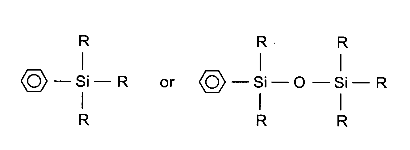
- the phenyl-based alkoxysilane compound has the general formula wherein R may comprise an O x C y H z substituent, such that x has a range between 0 and 3, y has a range between 0 and 6, and z has a range between 1 and 30.
- phenyltriethoxysilane SiO 3 C 12 H 20
- phenyltrimethoxysilane SiO 3 C 9 H 14
- diphenyldiethoxysilane SiO 2 C 16 H 20
- diphenyldimethoxysilane SiO 2 C 14 H 16
- the gas mixture may optionally include an organosilane compound having the general formula wherein R may comprise an O x C y H z substituent, such that x has a range between 0 and 3, y has a range between 0 and 6, and z has a range between 1 and 30.
- R may comprise an O x C y H z substituent, such that x has a range between 0 and 3, y has a range between 0 and 6, and z has a range between 1 and 30.
- the gas mixture may optionally include an oxygen-containing gas.
- Oxygen (O 2 ), ozone (O 3 ), nitrous oxide (N 2 O), carbon monoxide (CO), carbon dioxide (CO 2 ), or combinations thereof, among others, may be used as the oxygen-containing gas.
- the gas mixture may also include an inert gas.
- Argon Argon
- He helium
- Ne neon
- Xe xenon
- N 2 nitrogen
- the following deposition process parameters can be used to form the organosilicate layer using a CVD process chamber similar to that shown in FIG. 2.
- the process parameters may include a wafer temperature of about 50 °C to about 500 °C, a chamber pressure of about 1 torr to about 500 torr, a phenyl-based alkoxysilane compound gas flow rate of about 10 milligrams/minute (mgm) to about 1500 mgm, an organosilane compound flow rate of about 10 sccm to about 2000 sccm, an oxygen-containing gas flow rate of about 10 sccm to about 2000 sccm, an inert gas flow rate of about 1 sccm to about 10000 sccm, and an RF power of between about 1 watts/cm 2 to about 1500 watts/cm 2 .
- the above process parameters provide a deposition rate for the organosilicate layer in the range of about 500 ⁇ /min to about 20000 ⁇ /min when implemented on a 200 mm (millimeter) substrate in a deposition chamber available from Applied Materials, Inc., Santa Clara, California.
- deposition chambers are within the scope of the invention, and the parameters listed above may vary according to the particular deposition chamber used to form the organosilicate layer.
- other deposition chambers may have a larger (e.g. configured to accommodate 300 mm substrates) or smaller volume, requiring gas flow rates that are larger or smaller than those recited for deposition chambers available from Applied Materials, Inc.
- the as-deposited organosilicate layer has a dielectric constant that is less than about 3.0, making it suitable for use as an insulating material in integrated circuits.
- the dielectric constant of the organosilicate layer is tunable, in that it can be varied in the desired range as a function of the reaction temperature. In particular, as the temperature increases the dielectric constant of the as-deposited layer decreases.
- the dielectric constant of the organosilicate layer can also be tuned as a function of the composition of the gas mixture during layer formation. As the carbon (C) concentration in the gas mixture increases, the C content of the as-deposited organosilicate layer similarly increases, decreasing its dielectric constant.
- the organosilicate layer also has an absorption coefficient that is tunable in a range of about 0.1 to about 0.7 at wavelengths less than about 250 nm.
- the absorption coefficient is tunable as a function of the reaction temperature. In particular, as the temperature increases the absorption coefficient of the as-deposited layer increases.
- FIGs. 3a-3e illustrate schematic cross-sectional views of a substrate 300 at different stages of an integrated circuit fabrication sequence incorporating an organosilicate layer as an anti-reflective coating (ARC).
- the substrate 300 refers to any workpiece on which film processing is performed, and a substrate structure 350 is used to generally denote the substrate 300 together with other material layers formed on the substrate 300.
- the substrate 300 may correspond to a silicon wafer, or other material layer, which has been formed on the substrate.
- FIG. 3a illustrates a cross-sectional view of a substrate structure 350 in which the substrate 300 is a silicon wafer.
- An organosilicate layer 302 is formed on the substrate structure 350.
- the organosilicate layer 302 is formed on the substrate structure 350 according to the process parameters described above.
- the organosilicate layer has an absorption coefficient ( ⁇ ) that can be varied between about 0.1 to about 0.7 at wavelengths below about 250 nm (nanometers), making it suitable for use as an anti-reflective coating (ARC) at deep ultraviolet (DUV) wavelengths.
- ARC anti-reflective coating
- DUV deep ultraviolet
- the absorption coefficient of the organosilicate layer is tunable, in that it can be varied in the desired range as a function of the deposition temperature as well as the carbon concentration in the gas mixture during layer formation.
- the thickness of the organosilicate layer 302 is variable depending on the specific stage of processing. Typically, the organosilicate layer has a thickness of about 200 ⁇ to about 2000 ⁇ .
- FIG. 3b depicts a layer of energy sensitive resist material 304 formed on the substrate structure 350 of FIG. 3a.
- the layer of energy sensitive resist material may be spin coated on the substrate structure 350 to a thickness within a range of about 2000 ⁇ to about 6000 ⁇ .
- the energy sensitive resist material is sensitive to DUV radiation having a wavelength less than about 250 nm.
- An image of a pattern is introduced into the layer of energy sensitive resist material 304 by exposing such energy sensitive resist material 304 to DUV radiation via mask 306.
- the organosilicate layer 302 suppresses any reflections off underlying material layers (e. g., oxides, metals). Such reflections can degrade the image of the pattern introduced in the layer of energy sensitive resist material 304.
- the image of the pattern introduced into the layer of energy sensitive resist material 304 is developed in an appropriate developer to define the pattern therethrough, as shown in FIG. 3c. Thereafter, referring to FIG. 3d, the pattern defined in the energy sensitive resist material 304 is transferred through the organosilicate layer 302.
- the pattern is transferred through the organosilicate layer 302 using the energy sensitive resist material 304 as a mask.
- the pattern is transferred through the organosilicate layer 302 by etching it using an appropriate chemical etchant (e.g., carbon tetrafluoride (CF 4 ) or a gas mixture comprising trifluoromethane, fluoroethane, or fluorobutene (CHF3) and oxygen (O 2 )).
- an appropriate chemical etchant e.g., carbon tetrafluoride (CF 4 ) or a gas mixture comprising trifluoromethane, fluoroethane, or fluorobutene (CHF3) and oxygen (O 2
- Fig. 3e illustrates the completion of the integrated circuit fabrication sequence by the transfer of the pattern defined in the organosilicate layer 302 into the substrate 300.
- the pattern is transferred into the substrate 300 using the organosilicate layer 302 as a hardmask.
- the pattern is transferred into the substrate 300 by etching the substrate 300 using an appropriate chemical etchant (e.g., CF 4 ).
- the organosilicate layer 302 can optionally be stripped from the substrate structure 350 by etching it using an appropriate chemical etchant (e. g., carbon tetrafluoride CF 4 ), or a gas mixture comprising trifluoromethane (CHF 3 ) and oxygen (O 2 )).
- an appropriate chemical etchant e. g., carbon tetrafluoride CF 4
- a gas mixture comprising trifluoromethane (CHF 3 ) and oxygen (O 2 )
- FIGS. 4a-4e illustrate schematic cross-sectional views of a substrate 400 at different stages of an integrated circuit fabrication sequence incorporating an organosilicate layer as a hard mask.
- the substrate 400 refers to any workpiece on which processing is performed, and the substrate structure 450 is used to generally denote the substrate together with other material layers formed on the substrate 400.
- the substrate 400 may correspond to a silicon substrate, or other material layer that has been formed on the substrate.
- FIG. 4a illustrates a cross-sectional view of a substrate structure 450, having a material layer 402 formed thereon.
- the material layer 402 may be an oxide (e. g., silicon dioxide).
- the substrate 400 may include a layer of silicon, silicides, metals, or other materials.
- FIG. 4a illustrates one embodiment in which the substrate 400 is silicon having a silicon dioxide layer formed thereon.
- FIG. 4b depicts an organosilicate layer 404 formed on the substrate structure 450 of FIG. 4a.
- the organosilicate layer 404 is formed on the substrate structure 450 according to the process parameters described above.
- the thickness of the organosilicate layer 400 is variable depending on the specific stage of processing. Typically, the organosilicate layer 404 is deposited to a thickness of about 200 ⁇ to about 2000 ⁇ .
- a layer of energy sensitive resist material 408 is formed on the organosilicate layer 404.
- the layer of energy sensitive resist material 408 can be spin coated on the substrate to a thickness within a range of about 4,000 ⁇ to about 10,000 ⁇ .
- Most energy sensitive resist materials are sensitive to ultraviolet (UV) radiation having a wavelength less than about 450 nm (nanometers).
- Deep ultraviolet (DUV) resist materials are sensitive to UV radiation having wavelengths less than about 245 nm.
- an intermediate layer 406 is formed on the organosilicate layer 404 prior to the layer of energy sensitive resist material 408.
- the intermediate layer 406 functions as a mask for the organosilicate layer 404.
- the intermediate layer 406 may be conventionally formed on the organosilicate layer 404.
- the intermediate layer 406 may be an oxide, nitride, silicon oxynitride, amorphous silicon, or other suitable material.
- An image of a pattern is introduced into the layer of energy sensitive resist material 408 by exposing such energy sensitive resist material 408 to DUV radiation via mask 410.
- the image of the pattern introduced in the layer of energy sensitive resist material 408 is developed in an appropriate developer to define the pattern therethrough, as shown in FIG. 4c.
- the pattern defined in the energy sensitive resist material 408 is transferred through the organosilicate layer 404 using the energy sensitive resist material 408 as a mask.
- the pattern is transferred through the organosilicate layer 404 using an appropriate chemical etchant.
- fluorocarbon compounds such as carbon tetrafluoride (CF 4 ), fluoroethane (C 2 F 6 ), and fluorobutene (C 4 F 8 ) may be used to chemically etch the organosilicate layer 404.
- the pattern defined in the energy sensitive resist material 408 is first transferred through the intermediate layer 406 using the energy sensitive resist material 408 as a mask. Thereafter, the pattern is transferred through the organosilicate layer 404 using the intermediate layer 406 as a mask. The pattern is transferred through both the intermediate layer 406 as well as the organosilicate layer 404 using the appropriate chemical etchants.
- FIG. 4e illustrates the completion of the integrated circuit fabrication sequence by the transfer of the pattern defined in the organosilicate layer 404 through the silicon dioxide layer 402 using the organosilicate layer 404 as a hardmask.
- the organosilicate layer 404 can optionally be stripped from the substrate 400 by etching it using a suitable chemical etchant.
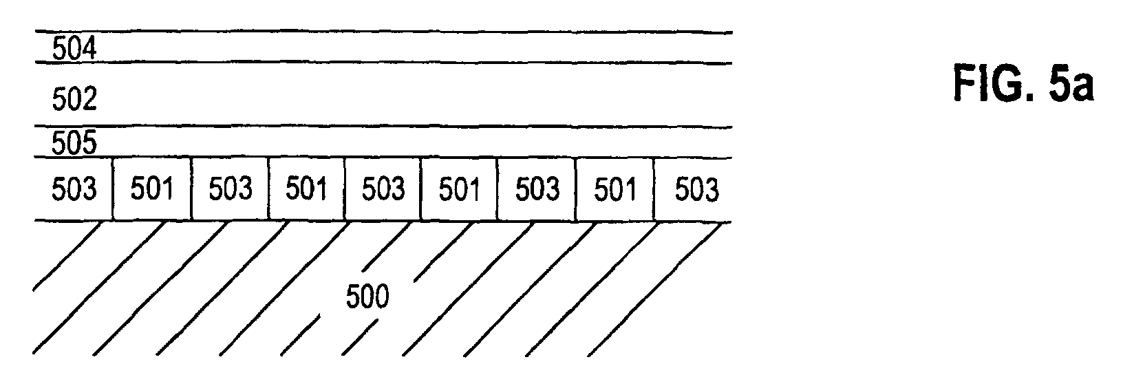
- FIGS. 5a-5e illustrate schematic cross-sectional views of a substrate 500 at different stages of a damascene structure fabrication sequence incorporating an organosilicate layer therein. Damascene structures are typically used to form metal interconnects on integrated circuits.
- substrate 500 may correspond to a silicon substrate, or other material layers that have been formed on the substrate 500.
- FIG. 5a illustrates a cross-sectional view of a substrate 500 having conductive features 501, intermetal dielectric 503, a barrier layer 505, as well as a first dielectric layer 502 formed thereon.
- the conductive features 501 may be a metal (e. g., aluminum, copper).
- the intermetal dielectric 503 and the barrier layer 505 may be a low dielectric constant material (e. g., organosilicate material, silicon carbide).
- the first dielectric layer 502 may be an oxide (e. g., silicon dioxide, fluorosilicate glass).
- the substrate 500 may include a layer of silicon, silicides, metals, or other materials.
- FIG. 5a illustrates one embodiment in which the substrate 500 is silicon, the conductive features 501 are copper, the intermetal dielectric 503 silicon oxide, and the first dielectric layer 502 is a fluorosilicate glass.
- the first dielectric layer 502 has a thickness of about 1,000 ⁇ to about 10,000 ⁇ , depending on the size of the structure to be fabricated.
- An organosilicate layer 504 is formed on the first dielectric layer 502.
- the organosilicate layer 504 is formed on the first dielectric layer 502 according to the process parameters described above.
- the organosilicate layer 504 has a dielectric constant less than about 3.0, so as to prevent or minimize capacitive coupling between the metal interconnects to be formed in the damascene structure.
- the dielectric constant for the organosilicate layer is tunable, in that it can be varied in the desired range as a function of the reaction temperature as well as the composition of the gas mixture during layer formation.
- the thickness of the organosilicate layer 504 is variable depending on the specific stage of processing. Typically, the organosilicate layer 504 has a thickness of about 200 ⁇ to about 1000 ⁇ , depending on its dielectric constant as well as its etch selectivity with respect to an overlying dielectric material subsequently formed thereon (e. g., the barrier layer preferably has an etch selectivity with respect to the overlying dielectric layer that is greater than about 10:1).
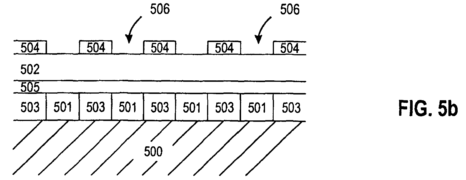
- the organosilicate layer 504 is patterned and etched to define contact/via openings 506 and to expose the first dielectric layer 502, in areas where the contacts/vias are to be formed.
- the contact/via openings 506 are positioned over the conductive features 501.
- the organosilicate layer 504 is patterned using conventional lithography (as described above with reference to FIGS. 4b-4d) and etched using fluorocarbon compounds such as fluoromethane (CF 4 ), fluoroethane (C 2 F 6 ), fluorobutene (C 4 F 8 ), and combinations thereof.
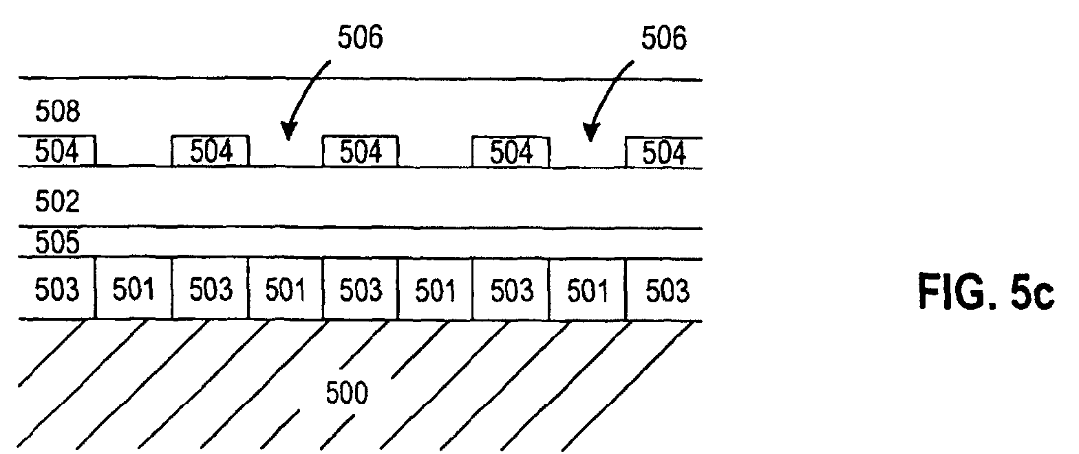
- a second dielectric layer 508 is deposited over the organosilicate layer 504, as shown in FIG. 5c.
- the second dielectric layer 508 may be an oxide (e. g., silicon dioxide, fluorosilicate glass).
- the second dielectric layer 508 has a thickness of about 1,000 ⁇ to about 10,000 ⁇ , depending on the size of the structure to be fabricated.
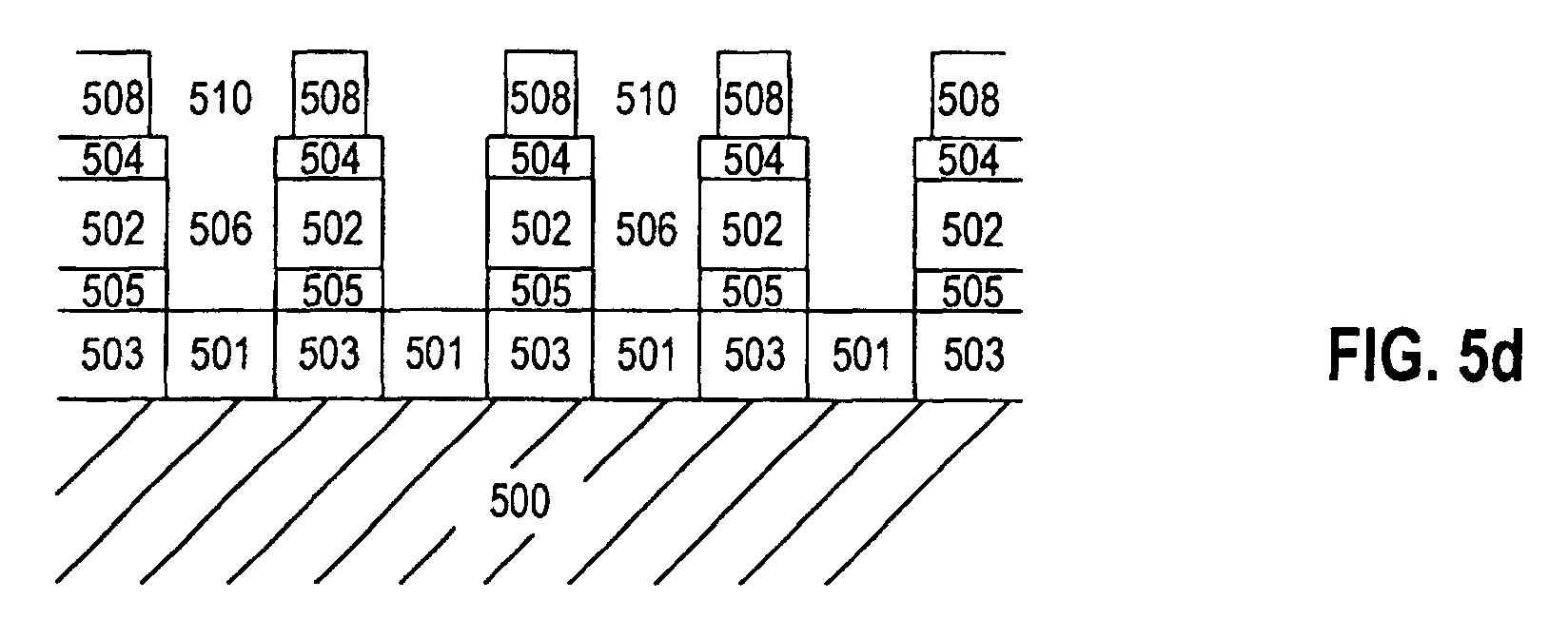
- the second dielectric layer 508 is then patterned to define interconnects 510, as illustrated in FIG. 5d, preferably using conventional lithography processes as described above.
- the interconnects 510 formed in the second dielectric layer 508 are positioned over the contact/via openings 506 in the organosilicate layer 504. Thereafter, both the interconnects 510 and contacts/vias 506 are etched to expose the surface of the conductive features 501, using reactive ion etching or other anisotropic etching techniques.
- the interconnects 510 and contacts/vias 506 are filled with a conductive material 514 such as aluminum (Al), copper (Cu), tungsten (W), or combinations thereof.
- a conductive material 514 such as aluminum (Al), copper (Cu), tungsten (W), or combinations thereof.
- Al aluminum
- Cu copper
- W tungsten
- copper is used to fill the interconnects 510 and contacts/vias 506 due to its low resistivity (resistivity about 1.7 ⁇ -cm).
- the conductive material 514 is deposited using chemical vapor deposition, physical vapor deposition, electroplating, or combinations thereof, to form the damascene structure.
- a barrier layer 512 such as tantalum, tantalum nitride, or other suitable barrier material is first deposited conformably on the sidewalls of the interconnects 510 and contacts/vias 506 to prevent metal migration into the surrounding dielectric layers 502, 508 as well as the organosilicate layer 504.
Landscapes
- Chemical & Material Sciences (AREA)
- Mechanical Engineering (AREA)
- General Chemical & Material Sciences (AREA)
- Chemical Kinetics & Catalysis (AREA)
- Engineering & Computer Science (AREA)
- Materials Engineering (AREA)
- Inorganic Chemistry (AREA)
- Metallurgy (AREA)
- Organic Chemistry (AREA)
- Formation Of Insulating Films (AREA)
- Internal Circuitry In Semiconductor Integrated Circuit Devices (AREA)
- Chemical Vapour Deposition (AREA)
- Silicon Polymers (AREA)
Abstract
Description

Claims (34)
- A method of thin film deposition, comprising:positioning a substrate in a deposition chamber;providing a gas mixture to the deposition chamber, wherein the gas mixture comprises a phenyl-based alkoxysilane compound; andreacting the gas mixture to form an organosilicate layer on the substrate.
- The method of claim 1 wherein the thin film deposition comprises forming an organosilicate layer on a substrate.
- A method of forming a device, comprising:forming an organosilicate layer on a substrate,
wherein the organosilicate layer is formed by reacting a gas mixture comprising a phenyl-based alkoxysilane compound in a deposition chamber; anddefining a pattern in at least one region of the organosilicate layer. - The method of claim 3 further comprising transferring the pattern defined in the at least one region of the organosilicate layer into the substrate using the organosilicate layer as a mask.
- The method of claim 3 or 4 further comprising the step of removing the organosilicate layer from the substrate.
- The method of claim 1 to 3 wherein the substrate has one or more material layers formed thereon.
- The method of claim 3 wherein definition of the pattern in at least one region of the organosilicate layer, comprises:forming a layer of energy sensitive resist material on the organosilicate layer;introducing an image of the pattern into the layer of energy sensitive resist material by exposing the energy sensitive resist material to patterned radiation;developing the image of the pattern introduced into the layer of energy sensitive resist material; andtransferring the pattern through the organosilicate layer using the layer of energy sensitive resist material as a mask.
- The method of claim 7 further comprising:forming an intermediate layer on the organosilicate layer prior to forming the layer of energy sensitive resist thereon, introducing the image of a pattern therein, and developing the pattern;transferring the image of the pattern developed in the layer of energy sensitive resist material through the intermediate layer using the energy sensitive resist material as a mask; andtransferring the pattern through the organosilicate layer using the intermediate layer as a mask.
- The method of claim 8 wherein the intermediate layer is an oxide the oxide being preferably selected from the group of silicon dioxide, fluorosilicate glass (FSG), and silicon oxynitride.
- The method of claim 5 wherein the organosilicate layer is removed from the substrate using a fluorine-based compound the fluorine-based compound being preferably selected from the group of carbon tetrafluoride (CF4), fluoromethane (CFH3), fluoroethane (C2F6), fluorobutene (C4F8), and combinations thereof.
- The method of claim 3 wherein the organosilicate layer is an anti-reflective coating at wavelengths less than about 250 nm (nanometers).
- A method of fabricating a damascene structure, comprising:forming a first dielectric layer on a substrate;forming an organosilicate layer on the first dielectric layer, wherein the organosilicate layer is formed by reacting a gas mixture comprising a phenyl-based alkoxysilane compound in a deposition chamber;patterning the organosilicate layer to define contacts/vias therethrough;forming a second dielectric layer on the patterned organosilicate layer;patterning the second dielectric layer to define interconnects therethrough, wherein the interconnects are positioned over the contacts/vias defined in the organosilicate layer;etching the first dielectric layer to form contacts/vias therethrough; andfilling the contacts/vias and the interconnects with a conductive material.
- The method of claim 12 wherein the first dielectric layer and the second dielectric layer are each selected from the group consisting of amorphous carbon, fluorinated amorphous carbon, parylene, fluorinated silicate glass (FSG), AF4, BCB, silicon carbide, oxynitride, and combinations thereof.
- The method of claim 12 wherein the conductive material filling the contacts/vias and interconnects is selected from the group of copper (Cu), aluminum (Al), tungsten (W), and combinations thereof.
- The method of claim 12 wherein the gas mixture further comprises an oxygen-containing gas.
- The method of claim any of the claim 1 to 3 or 12 wherein the gas mixture is reacted by applying an electric field to the gas mixture in the deposition chamber.
- The method of claim any of the claim 1 to 3 or 12 wherein the gas mixture further comprises an organosilane compound.
- The method of claim any of the claim 1 to 3 or 12 wherein the phenyl-based alkoxysilane compound has the general formulawherein R comprises an OxCyHz constituent, and wherein x has a range between 0 and 3, y has a range between 0 and 6, and z has a range between 1 and 30.

- The method of claim 18 wherein the phenyl-based alkoxysilane compound is selected from the group of phenyltriethoxysilane (SiO3C12H20), phenyltrimethoxysilane (SiO3C9H14), diphenyldiethoxysilane (SiO2C16H20), diphenyldimethoxysilane (SiO2C14H16), and combinations thereof.
- The method of claim 17 wherein the organosilane compound has the general formulawherein R comprises an OxCyHz substituent, and wherein x has a range between 0 and 3, y has a range between 0 and 6, and z has a range between 1 and 30.

- The method of claim 20 wherein the organosilane compound is selected from the group of trimethylsilane (SiC3H10), triethylsilane (SiC6H16), methylsilane (SiCH6), dimethylsilane (SiC2H8), tetramethylsilane (SiC4H12), methoxysilane (SiCH6O), dimethyldimethoxysilane (SiC4H12O2), diethyldiethoxysilane (SiC8H20O2), dimethyldiethoxysilane (SiC6H16O2), diethyldiethoxysilane (SiC6H16O2), hexamethyldisiloxane (Si2C6H18O), bis(methylsilano)methane (Si2C3H12), 1,2-bis(methylsilano)ethane (Si2C4H14), and combinations thereof.
- The method of claim any of the claim 1 to 3 or 12 wherein the gas mixture further comprises an oxygen-containing gas, the oxygen-containing gas being preferably selected from the group of nitrous oxide (N2O), oxygen (O2), ozone (O3), carbon monoxide (CO), carbon dioxide (CO2), and combinations thereof.
- The method of claim 16 wherein the electric field applied to the gas mixture in the deposition chamber is a radio frequency (RF) power, the RF power being preferably within the range of about 1 watts/cm2 to about 1500 watts/cm2.
- The method of claim any of the claim 1 to 3 or 12 wherein the deposition chamber is maintained at a pressure between about 1 torr to about 500 torr.
- The method of claim any of the claim 1 to 3 or 12 wherein the phenyl-based alkoxysilane compound is provided to the deposition chamber at a flow rate in a range of about 10 mgm (milligrams/minute) to about 1500 mgm.
- The method of any of the claim 1 to 3 or 12 wherein the organosilane compound is provided to the deposition chamber at a flow rate in a range of about 10 sccm to about 2000 sccm.
- The method of claim 22 wherein the oxygen-containing gas is provided to the deposition chamber at a flow rate in a range of about 10 sccm to about 2000 sccm.
- The method of claim any of the claim 1 to 3 or 12 wherein the deposition chamber is maintained at a temperature between about 50 °C to about 500 °C.
- The method of claim any of the claim 1 to 3 or 12 wherein the gas mixture further comprises an inert gas, the inert gas being preferably selected from the group of helium (He), argon (Ar), neon (Ne), xenon (Xe), nitrogen (N2), and combinations thereof.
- The method of claim 29 wherein the inert gas is provided to the deposition chamber at a flow rate in a range of about 1 sccm to about 10000 sccm.
- The method of any of the preceding claims wherein the organosilicate layer has an absorption coefficient in a range of about 0.1 to about 0.7 at wavelengths less than about 250 nm.
- The method of any of the preceding claims wherein the organosilicate layer has a dielectric constant less than about 3.0.
- The method of any of the preceding claims wherein the organosilicate layer has an index of refraction in a range of about 1.2 to about 1.7.
- A computer storage medium containing a software routine that, when executed, causes a general purpose computer to control a deposition chamber according to a method as claimed in any of preceding claims.
Applications Claiming Priority (2)
| Application Number | Priority Date | Filing Date | Title |
|---|---|---|---|
| US09/723,886 US6500773B1 (en) | 2000-11-27 | 2000-11-27 | Method of depositing organosilicate layers |
| US723886 | 2000-11-27 |
Publications (2)
| Publication Number | Publication Date |
|---|---|
| EP1209728A2 true EP1209728A2 (en) | 2002-05-29 |
| EP1209728A3 EP1209728A3 (en) | 2004-10-27 |
Family
ID=24908107
Family Applications (1)
| Application Number | Title | Priority Date | Filing Date |
|---|---|---|---|
| EP01124607A Withdrawn EP1209728A3 (en) | 2000-11-27 | 2001-10-15 | Method of depositing organosilicate layers |
Country Status (6)
| Country | Link |
|---|---|
| US (1) | US6500773B1 (en) |
| EP (1) | EP1209728A3 (en) |
| JP (1) | JP4709450B2 (en) |
| KR (1) | KR100849573B1 (en) |
| SG (1) | SG102010A1 (en) |
| TW (1) | TW552308B (en) |
Cited By (6)
| Publication number | Priority date | Publication date | Assignee | Title |
|---|---|---|---|---|
| WO2004055881A1 (en) * | 2002-12-13 | 2004-07-01 | Applied Materials, Inc. | Nitrogen-free dielectric anti-reflective coating and hardmask |
| EP1489197A1 (en) * | 2003-06-17 | 2004-12-22 | Semiconductor Process Laboratory Co., Ltd. | Method of manufacturing semiconductor device |
| WO2005048329A1 (en) | 2003-11-06 | 2005-05-26 | Tokyo Electron Limited | Method for depositing materials on a substrate |
| US6927178B2 (en) | 2002-07-11 | 2005-08-09 | Applied Materials, Inc. | Nitrogen-free dielectric anti-reflective coating and hardmask |
| US7105460B2 (en) | 2002-07-11 | 2006-09-12 | Applied Materials | Nitrogen-free dielectric anti-reflective coating and hardmask |
| CN100481344C (en) * | 2002-12-13 | 2009-04-22 | 应用材料有限公司 | Nitrogen-free dielectric anti-reflective coating and hardmask |
Families Citing this family (32)
| Publication number | Priority date | Publication date | Assignee | Title |
|---|---|---|---|---|
| US6303523B2 (en) | 1998-02-11 | 2001-10-16 | Applied Materials, Inc. | Plasma processes for depositing low dielectric constant films |
| US6287990B1 (en) * | 1998-02-11 | 2001-09-11 | Applied Materials, Inc. | CVD plasma assisted low dielectric constant films |
| US6759327B2 (en) * | 2001-10-09 | 2004-07-06 | Applied Materials Inc. | Method of depositing low k barrier layers |
| US6699784B2 (en) | 2001-12-14 | 2004-03-02 | Applied Materials Inc. | Method for depositing a low k dielectric film (K>3.5) for hard mask application |
| US7091137B2 (en) | 2001-12-14 | 2006-08-15 | Applied Materials | Bi-layer approach for a hermetic low dielectric constant layer for barrier applications |
| US6890850B2 (en) | 2001-12-14 | 2005-05-10 | Applied Materials, Inc. | Method of depositing dielectric materials in damascene applications |
| US6838393B2 (en) * | 2001-12-14 | 2005-01-04 | Applied Materials, Inc. | Method for producing semiconductor including forming a layer containing at least silicon carbide and forming a second layer containing at least silicon oxygen carbide |
| US20030194495A1 (en) * | 2002-04-11 | 2003-10-16 | Applied Materials, Inc. | Crosslink cyclo-siloxane compound with linear bridging group to form ultra low k dielectric |
| US7060330B2 (en) | 2002-05-08 | 2006-06-13 | Applied Materials, Inc. | Method for forming ultra low k films using electron beam |
| US7056560B2 (en) * | 2002-05-08 | 2006-06-06 | Applies Materials Inc. | Ultra low dielectric materials based on hybrid system of linear silicon precursor and organic porogen by plasma-enhanced chemical vapor deposition (PECVD) |
| US6936551B2 (en) | 2002-05-08 | 2005-08-30 | Applied Materials Inc. | Methods and apparatus for E-beam treatment used to fabricate integrated circuit devices |
| US7749563B2 (en) | 2002-10-07 | 2010-07-06 | Applied Materials, Inc. | Two-layer film for next generation damascene barrier application with good oxidation resistance |
| US6790788B2 (en) | 2003-01-13 | 2004-09-14 | Applied Materials Inc. | Method of improving stability in low k barrier layers |
| US6897163B2 (en) * | 2003-01-31 | 2005-05-24 | Applied Materials, Inc. | Method for depositing a low dielectric constant film |
| US7199046B2 (en) * | 2003-11-14 | 2007-04-03 | Tokyo Electron Ltd. | Structure comprising tunable anti-reflective coating and method of forming thereof |
| KR100857297B1 (en) * | 2004-03-01 | 2008-09-05 | 도쿄엘렉트론가부시키가이샤 | Processing method of substrate and rec0rding medium memorizing program to control the same |
| US7030041B2 (en) | 2004-03-15 | 2006-04-18 | Applied Materials Inc. | Adhesion improvement for low k dielectrics |
| US20050214457A1 (en) * | 2004-03-29 | 2005-09-29 | Applied Materials, Inc. | Deposition of low dielectric constant films by N2O addition |
| US7229911B2 (en) | 2004-04-19 | 2007-06-12 | Applied Materials, Inc. | Adhesion improvement for low k dielectrics to conductive materials |
| US7271093B2 (en) | 2004-05-24 | 2007-09-18 | Asm Japan K.K. | Low-carbon-doped silicon oxide film and damascene structure using same |
| US7288205B2 (en) | 2004-07-09 | 2007-10-30 | Applied Materials, Inc. | Hermetic low dielectric constant layer for barrier applications |
| US7259111B2 (en) * | 2005-01-19 | 2007-08-21 | Applied Materials, Inc. | Interface engineering to improve adhesion between low k stacks |
| US7425350B2 (en) * | 2005-04-29 | 2008-09-16 | Asm Japan K.K. | Apparatus, precursors and deposition methods for silicon-containing materials |
| US20070181420A1 (en) * | 2006-02-07 | 2007-08-09 | Ming-Tung Wang | Wafer stage having an encapsulated central pedestal plate |
| US7485573B2 (en) * | 2006-02-17 | 2009-02-03 | International Business Machines Corporation | Process of making a semiconductor device using multiple antireflective materials |
| US7972957B2 (en) * | 2006-02-27 | 2011-07-05 | Taiwan Semiconductor Manufacturing Company | Method of making openings in a layer of a semiconductor device |
| US7297376B1 (en) | 2006-07-07 | 2007-11-20 | Applied Materials, Inc. | Method to reduce gas-phase reactions in a PECVD process with silicon and organic precursors to deposit defect-free initial layers |
| KR102099712B1 (en) | 2013-01-15 | 2020-04-10 | 삼성전자주식회사 | Method of forming a pattern and method of manufacturing a semiconductor device using the same |
| KR101770718B1 (en) | 2014-12-12 | 2017-08-24 | (주)디엔에프 | Silicon precursor and manufacturing method of silicon-containing thin film using thereof |
| US20170125241A1 (en) * | 2015-10-30 | 2017-05-04 | Applied Materials, Inc. | Low temp single precursor arc hard mask for multilayer patterning application |
| US9793169B1 (en) * | 2016-06-07 | 2017-10-17 | Globalfoundries Inc. | Methods for forming mask layers using a flowable carbon-containing silicon dioxide material |
| US10998259B2 (en) * | 2017-08-31 | 2021-05-04 | Taiwan Semiconductor Manufacturing Company, Ltd. | Semiconductor device and method of manufacture |
Family Cites Families (13)
| Publication number | Priority date | Publication date | Assignee | Title |
|---|---|---|---|---|
| JPH07111957B2 (en) | 1984-03-28 | 1995-11-29 | 圭弘 浜川 | Semiconductor manufacturing method |
| US4894352A (en) | 1988-10-26 | 1990-01-16 | Texas Instruments Inc. | Deposition of silicon-containing films using organosilicon compounds and nitrogen trifluoride |
| JPH09326360A (en) * | 1996-03-07 | 1997-12-16 | Lucent Technol Inc | Device manufacturing method |
| US5989998A (en) * | 1996-08-29 | 1999-11-23 | Matsushita Electric Industrial Co., Ltd. | Method of forming interlayer insulating film |
| KR100463858B1 (en) * | 1996-08-29 | 2005-02-28 | 마츠시타 덴끼 산교 가부시키가이샤 | Method of forming interlayer insulating film |
| JP3226479B2 (en) * | 1996-08-29 | 2001-11-05 | 松下電器産業株式会社 | Method of forming interlayer insulating film |
| JP3173426B2 (en) * | 1997-06-09 | 2001-06-04 | 日本電気株式会社 | Method for manufacturing silica insulating film and method for manufacturing semiconductor device |
| TW437017B (en) * | 1998-02-05 | 2001-05-28 | Asm Japan Kk | Silicone polymer insulation film on semiconductor substrate and method for formation thereof |
| JP3726226B2 (en) * | 1998-02-05 | 2005-12-14 | 日本エー・エス・エム株式会社 | Insulating film and manufacturing method thereof |
| DE19904311A1 (en) | 1998-02-06 | 1999-08-12 | Nat Semiconductor Corp | Carbon-doped silicon oxide thin film to produce an insulating thin film for a semiconductor device |
| US6054379A (en) * | 1998-02-11 | 2000-04-25 | Applied Materials, Inc. | Method of depositing a low k dielectric with organo silane |
| US6068884A (en) * | 1998-04-28 | 2000-05-30 | Silcon Valley Group Thermal Systems, Llc | Method of making low κ dielectric inorganic/organic hybrid films |
| US6060132A (en) | 1998-06-15 | 2000-05-09 | Siemens Aktiengesellschaft | High density plasma CVD process for making dielectric anti-reflective coatings |
-
2000
- 2000-11-27 US US09/723,886 patent/US6500773B1/en not_active Expired - Fee Related
-
2001
- 2001-10-15 EP EP01124607A patent/EP1209728A3/en not_active Withdrawn
- 2001-10-16 TW TW090125612A patent/TW552308B/en not_active IP Right Cessation
- 2001-10-18 SG SG200106411A patent/SG102010A1/en unknown
- 2001-11-27 KR KR1020010074264A patent/KR100849573B1/en not_active Expired - Fee Related
- 2001-11-27 JP JP2001361102A patent/JP4709450B2/en not_active Expired - Fee Related
Cited By (9)
| Publication number | Priority date | Publication date | Assignee | Title |
|---|---|---|---|---|
| US6927178B2 (en) | 2002-07-11 | 2005-08-09 | Applied Materials, Inc. | Nitrogen-free dielectric anti-reflective coating and hardmask |
| US7105460B2 (en) | 2002-07-11 | 2006-09-12 | Applied Materials | Nitrogen-free dielectric anti-reflective coating and hardmask |
| WO2004055881A1 (en) * | 2002-12-13 | 2004-07-01 | Applied Materials, Inc. | Nitrogen-free dielectric anti-reflective coating and hardmask |
| CN100481344C (en) * | 2002-12-13 | 2009-04-22 | 应用材料有限公司 | Nitrogen-free dielectric anti-reflective coating and hardmask |
| EP1489197A1 (en) * | 2003-06-17 | 2004-12-22 | Semiconductor Process Laboratory Co., Ltd. | Method of manufacturing semiconductor device |
| US7238629B2 (en) | 2003-06-17 | 2007-07-03 | Semiconductor Process Laboratory Co., Ltd. | Deposition method, method of manufacturing semiconductor device, and semiconductor device |
| KR100746679B1 (en) * | 2003-06-17 | 2007-08-06 | 가부시끼가이샤 한도따이 프로세스 켄큐쇼 | Deposition method, method of manufacturing semiconductor device, and semiconductor device |
| WO2005048329A1 (en) | 2003-11-06 | 2005-05-26 | Tokyo Electron Limited | Method for depositing materials on a substrate |
| CN100490069C (en) * | 2003-11-06 | 2009-05-20 | 东京毅力科创株式会社 | Method for depositing materials on a substrate |
Also Published As
| Publication number | Publication date |
|---|---|
| SG102010A1 (en) | 2004-02-27 |
| KR20020041320A (en) | 2002-06-01 |
| TW552308B (en) | 2003-09-11 |
| JP4709450B2 (en) | 2011-06-22 |
| JP2002235172A (en) | 2002-08-23 |
| EP1209728A3 (en) | 2004-10-27 |
| US6500773B1 (en) | 2002-12-31 |
| KR100849573B1 (en) | 2008-07-31 |
Similar Documents
| Publication | Publication Date | Title |
|---|---|---|
| US6500773B1 (en) | Method of depositing organosilicate layers | |
| US6465366B1 (en) | Dual frequency plasma enhanced chemical vapor deposition of silicon carbide layers | |
| US6537733B2 (en) | Method of depositing low dielectric constant silicon carbide layers | |
| US7117064B2 (en) | Method of depositing dielectric films | |
| US6777171B2 (en) | Fluorine-containing layers for damascene structures | |
| US6531398B1 (en) | Method of depositing organosillicate layers | |
| US6841341B2 (en) | Method of depositing an amorphous carbon layer | |
| US6632735B2 (en) | Method of depositing low dielectric constant carbon doped silicon oxide | |
| US7244672B2 (en) | Selective etching of organosilicate films over silicon oxide stop etch layers | |
| US6573196B1 (en) | Method of depositing organosilicate layers | |
| EP1186685A2 (en) | Method for forming silicon carbide films | |
| EP1164632A2 (en) | Method of forming a fluoro-organosilicate layer on a substrate | |
| US20020142104A1 (en) | Plasma treatment of organosilicate layers |
Legal Events
| Date | Code | Title | Description |
|---|---|---|---|
| PUAI | Public reference made under article 153(3) epc to a published international application that has entered the european phase |
Free format text: ORIGINAL CODE: 0009012 |
|
| AK | Designated contracting states |
Kind code of ref document: A2 Designated state(s): AT BE CH CY DE DK ES FI FR GB GR IE IT LI LU MC NL PT SE TR |
|
| AX | Request for extension of the european patent |
Free format text: AL;LT;LV;MK;RO;SI |
|
| RIC1 | Information provided on ipc code assigned before grant |
Ipc: 7C 23C 16/40 B Ipc: 7C 23C 16/30 B Ipc: 7H 01L 21/027 B Ipc: 7H 01L 21/316 B Ipc: 7H 01L 21/312 A |
|
| PUAL | Search report despatched |
Free format text: ORIGINAL CODE: 0009013 |
|
| AK | Designated contracting states |
Kind code of ref document: A3 Designated state(s): AT BE CH CY DE DK ES FI FR GB GR IE IT LI LU MC NL PT SE TR |
|
| AX | Request for extension of the european patent |
Extension state: AL LT LV MK RO SI |
|
| 17P | Request for examination filed |
Effective date: 20050418 |
|
| AKX | Designation fees paid |
Designated state(s): AT BE CH CY DE DK ES FI FR GB GR IE IT LI LU MC NL PT SE TR |
|
| 17Q | First examination report despatched |
Effective date: 20050704 |
|
| STAA | Information on the status of an ep patent application or granted ep patent |
Free format text: STATUS: THE APPLICATION IS DEEMED TO BE WITHDRAWN |
|
| 18D | Application deemed to be withdrawn |
Effective date: 20051115 |