EP1207553A1 - Fixing device for pressure contacted high power semiconductor device - Google Patents
Fixing device for pressure contacted high power semiconductor device Download PDFInfo
- Publication number
- EP1207553A1 EP1207553A1 EP00811084A EP00811084A EP1207553A1 EP 1207553 A1 EP1207553 A1 EP 1207553A1 EP 00811084 A EP00811084 A EP 00811084A EP 00811084 A EP00811084 A EP 00811084A EP 1207553 A1 EP1207553 A1 EP 1207553A1
- Authority
- EP
- European Patent Office
- Prior art keywords
- state
- spring
- clamping device
- power semiconductor
- spring elements
- Prior art date
- Legal status (The legal status is an assumption and is not a legal conclusion. Google has not performed a legal analysis and makes no representation as to the accuracy of the status listed.)
- Withdrawn
Links
Images


Classifications
-
- H—ELECTRICITY
- H01—ELECTRIC ELEMENTS
- H01L—SEMICONDUCTOR DEVICES NOT COVERED BY CLASS H10
- H01L24/00—Arrangements for connecting or disconnecting semiconductor or solid-state bodies; Methods or apparatus related thereto
- H01L24/71—Means for bonding not being attached to, or not being formed on, the surface to be connected
- H01L24/72—Detachable connecting means consisting of mechanical auxiliary parts connecting the device, e.g. pressure contacts using springs or clips
-
- H—ELECTRICITY
- H01—ELECTRIC ELEMENTS
- H01L—SEMICONDUCTOR DEVICES NOT COVERED BY CLASS H10
- H01L2924/00—Indexing scheme for arrangements or methods for connecting or disconnecting semiconductor or solid-state bodies as covered by H01L24/00
- H01L2924/01—Chemical elements
- H01L2924/01005—Boron [B]
-
- H—ELECTRICITY
- H01—ELECTRIC ELEMENTS
- H01L—SEMICONDUCTOR DEVICES NOT COVERED BY CLASS H10
- H01L2924/00—Indexing scheme for arrangements or methods for connecting or disconnecting semiconductor or solid-state bodies as covered by H01L24/00
- H01L2924/01—Chemical elements
- H01L2924/01082—Lead [Pb]
Definitions
- the present invention relates to the field of power electronics. she relates to a clamping device for at least one high-performance semiconductor component according to the preamble of claim 1.
- Such a jig is e.g. known from US-A-4,672,422.
- High-power semiconductor components have long been known in which a or several active semiconductor chip (s) in a closed housing between metallic disks arranged and by external pressure from both sides electrically and thermally contacted (so-called press pack housing).
- press pack housing Examples for such press pack modules e.g. in US-A-5,726,466 or US-A-5,278,434 disclosed.
- the pressure on the semiconductor chip is corresponding Clamping device usually by a stack of disc springs built up. They exert a force of the order of magnitude in normal operation 500 - 1000 N on the semiconductor chip.
- the contact voltage of a dry contact is approximately inversely proportional to the root of the contact pressure. This means that during operation in the SCFM state the contact voltage after a quasi-stable phase first slowly, then faster and faster, begins to rise. Above a critical one Contact tension begins to melt parts of the spring assembly. This will the current path is interrupted. However, since the outer circuit is inductive in nature the voltage will rise very quickly and a next chip due to voltage overload fail. This next chip then goes into the SCFM condition. The process continues until all of the chips in the module are used up are.
- SCFM short circuit
- the object is achieved by the entirety of the features of claim 1.
- the essence of the invention is at least part of the spring elements from materials that belong to the group of shape memory alloys (Shape Memory Alloy, SMA) belong. Because of the special properties shape memory alloys, it is possible in a simple manner even in the event of a short circuit sufficient force on the power semiconductor component in the clamping device to exercise or maintain.
- a first group of SMA materials suitable for the invention is emerging characterized in that the elastic constant at a phase transition from one Low temperature phase (in normal operating condition) to a high temperature phase (in SCFM operating state) increases significantly.
- a preferred embodiment of the clamping device according to the invention is therefore characterized in that the material is in the temperature range, which prevails in normal operation, is in a first state and in one due to a short-circuit current elevated temperature in a second state compared to the first state of significantly increased spring force. The Phase transition thus takes place due to the temperature increase with the short circuit connected is.
- a preferred further development of this embodiment is characterized by that the at least one spring element made of the material from the group of Shape memory alloys in the first state is completely compressed and only expanded in the second state. This creates additional travel and an increase in spring force. But it is also conceivable that at least a spring element contributes to the spring travel in the normal state and through the phase transition increases the spring force.
- the spring elements are disc springs.
- disc springs made of normal spring materials and disc springs made of shape memory alloys arranged in a common spring stack. This results in a reliable, simple and effective pressure generation that saves space and can be easily integrated into conventional clamping devices
- a second group of SMA materials suitable for the invention shows this Superplasticity phenomenon.
- the spring force remains in the superplastic state a spring over a considerable spring travel almost independent of the spring travel, while in a normal spring the force is proportional to the way. In order to the spring force remains when the superplasticity is used, even with great expansion the spring is still almost the same as in the initial state.
- Another preferred embodiment of the clamping device according to the invention is therefore characterized in that the material is the phenomenon of Has superplasticity, and that the spring elements in the jig are arranged so that in the event of a short circuit at nominal current, the minimum a spring element made of the material from the group of shape memory alloys is located in the superplastic part of the stress-strain curve. It can also be achieved that the spring force despite the Melting and creeping processes in the short-circuit state caused expansion does not decrease significantly.
- this preferably takes on the power semiconductor component effective force when the spring elements are dilated by 1mm from the nominal normal state, less than 30%.
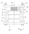
- Fig. 1 is a side view of a simplified embodiment reproduced for a jig according to the invention.
- the jig 10 comprises a lower holding plate 11 and an upper holding plate 20, the by bolts 21, 22 with threads and corresponding nuts 23, 24 with each other are connected (screwed).
- a stack is arranged and held, in the example shown from a high-performance semiconductor component 13 in the press pack housing and a lower and upper cooling box 12 and 16 respectively.
- the cooling boxes 12, 16 are flowed through by a coolant and carry the resulting in normal operation Heat loss from the high-power semiconductor device 13. You can can also be designed as power connections. It goes without saying also conceivable within the scope of the invention, several within the stack High-performance semiconductor components and cooling boxes alternately one above the other to arrange and connect the components in series, or the high-performance semiconductor component 13 with only one cooling box or with other cooling devices to combine.
- the internal (not visible) Semiconductor chip thermally and electrically through axially protruding electrode plates 14, 15 pressure-contacted.
- the necessary pressure is generated by a spring stack 25 generated from the first disc springs 18 and maintained in normal operation.
- the spring stack 25 is in the example shown between the upper cooling box 16 and the upper holding plate 20 and arranged from the upper cooling box 15 electrically insulated to avoid a short circuit by an insulating plate 17.
- each of the bolts 21, 22 to have its own spring stack assigned.
- second plate springs 19 made of a shape memory alloy are now provided in the spring stack 25.
- SMAs are below a critical temperature in a martensite structure. In the martensite phase, they are relatively soft and easily deformable. When heated, the SMA go through a phase transition (weak first order) into a more symmetrical austenite phase. In doing so, they deform back to their original state. The austenite phase has a high modulus of elasticity.
- Stacks of SMA disc springs with different transition temperatures have already been used for the stepwise generation of pressure in a different context (US-A-4,897,006).
- Braunovic and Labrecque in IEEE Transactions on Components, Packaging and Manufacturing Technology A, 19 , 295 (1996) suggested that Belleville washers (SMA-based) be used for stationary electrical contacts.
- the SMA material of the second disc springs 19 is now selected so that it is normal operating states of the high-power semiconductor component 13 in the Martensite phase is present. That means the transition temperature from the martensite the austenite phase must be above the maximum operating temperature of the springs lie in the intact state of the high-power semiconductor component 13. Furthermore, the second plate springs 19 are designed so that they are in the martensite phase are fully compressed (flat) (Fig. 1; curve A in Fig. 3; spring pressed in to travel s2; Spring force K1)). The spring action is thus in normal operation completely taken over by the first (normal) disc springs 18. Thereby there are no reliability problems related to the aging of the spring constant in the martensite phase.
- the second disc springs 19 (or all spring elements) from a material from the group of shape memory alloys to produce, which has the phenomenon of superplasticity.
- the spring elements are then designed and arranged in the clamping device 10, that in the event of a short circuit at nominal current in the superplastic part of the Stress-strain curve. It is particularly favorable if in the superplastic area that are based on the high-performance semiconductor component 13 effective force when the spring elements are dilated by 1mm, starting from nominal normal condition, decreasing less than 30%. This also makes it possible allow an expansion in the spring stack caused by the short circuit, without losing the necessary spring force.
Landscapes
- Engineering & Computer Science (AREA)
- Computer Hardware Design (AREA)
- Microelectronics & Electronic Packaging (AREA)
- Power Engineering (AREA)
- Springs (AREA)
Abstract
Description
Die vorliegende Erfindung bezieht sich auf das Gebiet der Leistungselektronik. Sie
betrifft eine Einspannvorrichtung für wenigstens ein Hochleistungshalbleiterbauelement
gemäss dem Oberbegriff des Anspruchs 1.The present invention relates to the field of power electronics. she
relates to a clamping device for at least one high-performance semiconductor component
according to the preamble of
Eine solche Einspannvorrichtung ist z.B. aus der US-A-4,672,422 bekannt.Such a jig is e.g. known from US-A-4,672,422.
Es sind seit langem Hochleistungshalbleiterbauelemente bekannt, bei denen ein oder mehrere aktive Halbleiterchip(s) in einem geschlossenen Gehäuse zwischen metallischen Scheiben angeordnet und durch beidseitigen Druck von aussen elektrisch und thermisch kontaktiert werden (sog. Presspack-Gehäuse). Beispiele für derartige Presspack-Module sind z.B. in der US-A-5,726,466 oder der US-A-5,278,434 offenbart.High-power semiconductor components have long been known in which a or several active semiconductor chip (s) in a closed housing between metallic disks arranged and by external pressure from both sides electrically and thermally contacted (so-called press pack housing). Examples for such press pack modules e.g. in US-A-5,726,466 or US-A-5,278,434 disclosed.
In heutigen Presspack-Modulen wird der Druck auf den Halbleiterchip in einer entsprechenden Einspannvorrichtung üblicherweise durch einen Stapel von Tellerfedern aufgebaut. Sie üben im Normalbetrieb eine Kraft in der Grössenordnung von 500 - 1000 N auf den Halbleiterchip aus.In today's press pack modules, the pressure on the semiconductor chip is corresponding Clamping device usually by a stack of disc springs built up. They exert a force of the order of magnitude in normal operation 500 - 1000 N on the semiconductor chip.
Fällt ein Chip (elektrisch) aus und geht in den Kurzschlusszustand (sog. Short Circuit Failure Mode oder kurz SCFM) über, so konzentriert sich der ganze Strom des Moduls auf den defekten Chip. Als Folge davon schmelzen bei Nennstrombedingungen Teile des Si-Chips auf und legieren mit den Kontaktpartnern, insbesondere den Druck ausübenden metallischen Scheiben. Andere Teile zeigen unter der stark erhöhten Betriebstemperatur des SCFM-Zustandes ein ausgeprägtes Kriechverhalten. Dadurch expandieren die Tellerfedern und die Kraft nimmt ab. Die Deformation kann sogar den zur Verfügung stehenden Federweg überschreiten, so dass die Kraft auf Null absinkt.If a chip fails (electrically) and goes into the short circuit state (so-called short circuit Failure Mode or SCFM for short), so the whole stream of the Module on the defective chip. As a result, melt at nominal current conditions Parts of the Si chip and alloy with the contact partners, in particular the pressure-exerting metallic disks. Other parts show below the pronounced increased operating temperature of the SCFM state Creep. As a result, the plate springs expand and the force decreases. The deformation can even exceed the available travel so that the force drops to zero.
Die Kontaktspannung eines Trockenkontakts ist ungefähr umgekehrt proportional zur Wurzel der Anpresskraft. Das führt dazu, dass während des Betriebes im SCFM-Zustand die Kontaktspannung nach einer quasi-stabilen Phase zuerst langsam, dann immer schneller, zu steigen beginnt. Oberhalb einer kritischen Kontaktspannung beginnen Teile des Federpaketes zu schmelzen. Dadurch wird der Strompfad unterbrochen. Da jedoch der äussere Schaltkreis induktiver Natur ist, wird die Spannung sehr rasch ansteigen und ein nächster Chip durch Spannungsüberbelastung ausfallen. Dieser nächste Chip geht dann seinerseits in den SCFM Zustand. Der Prozess setzt sich fort, bis alle Chips im Modul aufgebraucht sind.The contact voltage of a dry contact is approximately inversely proportional to the root of the contact pressure. This means that during operation in the SCFM state the contact voltage after a quasi-stable phase first slowly, then faster and faster, begins to rise. Above a critical one Contact tension begins to melt parts of the spring assembly. This will the current path is interrupted. However, since the outer circuit is inductive in nature the voltage will rise very quickly and a next chip due to voltage overload fail. This next chip then goes into the SCFM condition. The process continues until all of the chips in the module are used up are.
Um die Lebensdauer eines Chips im SCFM Zustand möglichst hoch zu halten, ist - insbesondere wenn der Nennstrom eines solchen Moduls in der Grössenordnung von 2000 A liegt - eine fortdauernde Anpresskraft des Kontaktes von minimal 1000 N unabdingbar.In order to keep the lifespan of a chip in the SCFM state as long as possible, especially if the nominal current of such a module is of the order of magnitude of 2000 A - a continuous contact pressure of at least 1000 N indispensable.
Es ist daher Aufgabe der Erfindung, eine Einspannvorrichtung für druckkontaktierte Hochleistungshalbleiterbauelemente zu schaffen, bei welcher ein Abfall der Normalkraft auf den Chip im Kurzschluss(SCFM)-Zustand sicher vermieden wird.It is therefore an object of the invention to provide a clamping device for pressure-contacted To create high-performance semiconductor devices, in which a waste of Normal force on the chip in the short circuit (SCFM) state is safely avoided.
Die Aufgabe wird durch die Gesamtheit der Merkmale des Anspruchs 1 gelöst.
Der Kern der Erfindung besteht darin, mindestens einen Teil der Federelemente
aus Werkstoffen herzustellen die zur Gruppe der Formgedächtnislegierungen
(Shape Memory Alloy, SMA) gehören. Aufgrund der besonderen Eigenschaften
der Formgedächtnislegierungen ist es möglich, auf einfache Weise auch im Kurzschlussfall
in der Einspannvorrichtung eine ausreichend Kraft auf das Leistungshalbleiterbauelement
auszuüben bzw. aufrechtzuerhalten.The object is achieved by the entirety of the features of
Eine für die Erfindung geeignete erste Gruppe von SMA Werkstoffen zeichnet sich dadurch aus, dass die Elastizitätskonstante bei einem Phasenübergang von einer Tieftemperaturphase (im normalen Betriebszustand) zu einer Hochtemperaturphase (im SCFM Betriebszustand) wesentlich zunimmt.A first group of SMA materials suitable for the invention is emerging characterized in that the elastic constant at a phase transition from one Low temperature phase (in normal operating condition) to a high temperature phase (in SCFM operating state) increases significantly.
Eine bevorzugte Ausgestaltung der erfindungsgemässen Einspannvorrichtung ist daher dadurch gekennzeichnet, dass sich der Werkstoff im Temperaturbereich, der im Normalbetrieb vorherrscht, in einem ersten Zustand befindet und bei einer durch einen Kurzschlussstrom erhöhten Temperatur in einen zweiten Zustand mit gegenüber dem ersten Zustand wesentlich erhöhter Federkraft übergeht. Der Phasenübergang erfolgt also durch die Temperaturerhöhung, die mit dem Kurzschluss verbunden ist. A preferred embodiment of the clamping device according to the invention is therefore characterized in that the material is in the temperature range, which prevails in normal operation, is in a first state and in one due to a short-circuit current elevated temperature in a second state compared to the first state of significantly increased spring force. The Phase transition thus takes place due to the temperature increase with the short circuit connected is.
Eine bevorzugte Weiterbildung dieser Ausgestaltung zeichnet sich dadurch aus, dass das mindestens eine Federelement aus dem Werkstoff aus der Gruppe der Formgedächtnislegierungen im ersten Zustand völlig zusammengedrückt ist und erst im zweiten Zustand expandiert. Dadurch entsteht ein zusätzlicher Federweg und eine Erhöhung der Federkraft. Es ist aber auch denkbar, dass das wenigstens eine Federelement bereits im Normalzustand zum Federweg beiträgt und durch den Phasenübergang die Federkraft erhöht.A preferred further development of this embodiment is characterized by that the at least one spring element made of the material from the group of Shape memory alloys in the first state is completely compressed and only expanded in the second state. This creates additional travel and an increase in spring force. But it is also conceivable that at least a spring element contributes to the spring travel in the normal state and through the phase transition increases the spring force.
Eine andere Ausgestaltung der Einspannvorrichtung nach der Erfindung zeichnet sich dadurch aus, dass die Federelemente Tellerfedern sind. Hierbei sind Tellerfedern aus normalen Federwerkstoffen und Tellerfedern aus Formgedächtnislegierungen in einem gemeinsamen Federstapel angeordnet. Hierdurch ergibt sich eine funktionssichere, einfache und wirkungsvolle Druckerzeugung, die platzsparend ist und sich leicht in herkömmliche Einspannvorrichtungen integrieren lässtAnother embodiment of the clamping device according to the invention is distinguished is characterized in that the spring elements are disc springs. Here are disc springs made of normal spring materials and disc springs made of shape memory alloys arranged in a common spring stack. This results in a reliable, simple and effective pressure generation that saves space and can be easily integrated into conventional clamping devices
Eine für die Erfindung geeignete zweite Gruppe von SMA-Werkstoffen zeigt das Phänomen der Superplastizität. Im superplastischen Zustand bleibt die Federkraft einer Feder über einen beträchtlichen Federweg nahezu unabhängig vom Federweg, während in einer normalen Feder die Kraft proportional zum Weg ist. Damit bleibt die Federkraft bei Ausnützung der Superplastizität auch bei grosser Expansion der Feder immer noch nahezu gleich wie im Ausgangszustand.A second group of SMA materials suitable for the invention shows this Superplasticity phenomenon. The spring force remains in the superplastic state a spring over a considerable spring travel almost independent of the spring travel, while in a normal spring the force is proportional to the way. In order to the spring force remains when the superplasticity is used, even with great expansion the spring is still almost the same as in the initial state.
Eine weitere bevorzugte Ausgestaltung der erfindungsgemässen Einspannvorrichtung ist daher dadurch gekennzeichnet, dass der Werkstoff das Phänomen der Superplastizität aufweist, und dass die Federelemente in der Einspannvorrichtung so angeordnet sind, dass sich in einem Kurzschlussfall bei Nennstrom das mindestens eine Federelement aus dem Werkstoff aus der Gruppe der Formgedächtnislegierungen im superplastischen Teil der Spannungs-Dehnungs Kennlinie befindet. Auch damit kann erreicht werden, dass die Federkraft trotz der durch Schmelz- und Kriechvorgänge im Kurzschlusszustand hervorgerufenen Expansion nicht wesentlich abnimmt. Another preferred embodiment of the clamping device according to the invention is therefore characterized in that the material is the phenomenon of Has superplasticity, and that the spring elements in the jig are arranged so that in the event of a short circuit at nominal current, the minimum a spring element made of the material from the group of shape memory alloys is located in the superplastic part of the stress-strain curve. It can also be achieved that the spring force despite the Melting and creeping processes in the short-circuit state caused expansion does not decrease significantly.
Bevorzugt nimmt im superplastischen Bereich die auf das Leistungshalbleiterbauelement wirkende Kraft bei einer Dilatation der Federelemente um 1mm, ausgehend vom nominellen Normalzustand, weniger als 30% ab.In the superplastic area, this preferably takes on the power semiconductor component effective force when the spring elements are dilated by 1mm from the nominal normal state, less than 30%.
Die Erfindung soll nachfolgend anhand von Ausführungsbeispielen im Zusammenhang mit der Zeichnung näher erläutert werden. Es zeigen
- Fig. 1
- in der Seitenansicht ein vereinfacht dargestelltes Ausführungsbeispiel für eine Einspannvorrichtung nach der Erfindung mit einem Federstapel, der zwei Arten von Tellerfedern enthält, während des Normalbetriebes;
- Fig. 2
- die Einspannvorrichtung aus Fig. 1 im Kurzschlussfall mit den aktivierten zweiten Tellerfedern; und
- Fig. 3
- ein schematisiertes Diagramm für die bei den zweiten Tellerfedern stattfindende Kraft-Weg-Aenderung beim Uebergang vom Normalbetrieb (Kurve A; Martensitphase) zum Kurzschlussfall (Kurve B; Austenitphase).
- Fig. 1
- the side view of a simplified embodiment of a clamping device according to the invention with a spring stack, which contains two types of disc springs, during normal operation;
- Fig. 2
- the clamping device of Figure 1 in the event of a short circuit with the activated second plate springs. and
- Fig. 3
- a schematic diagram for the change in force and displacement taking place in the case of the second disc springs during the transition from normal operation (curve A; martensite phase) to the event of a short circuit (curve B; austenite phase).
In Fig. 1 ist in der Seitenansicht ein vereinfacht dargestelltes Ausführungsbeispiel
für eine Einspannvorrichtung nach der Erfindung wiedergegeben. Die Einspannvorrichtung
10 umfasst eine untere Halteplatte 11 und eine obere Halteplatte 20,
die durch Bolzen 21, 22 mit Gewinden und entsprechenden Muttern 23, 24 miteinander
verbunden (verschraubt) sind. Zwischen der unteren und oberen Halteplatte
11 bzw. 20 ist ein Stapel angeordnet und gehalten, der im dargestellten Beispiel
aus einem Hochleistungshalbleiterbauelement 13 im Presspack-Gehäuse und
einer unteren und oberen Kühldose 12 bzw. 16 besteht. Die Kühldosen 12, 16 sind
von einer Kühlflüssigkeit durchflossen und führen die im Normalbetrieb entstehende
Verlustwärme aus dem Hochleistungshalbleiterbauelement 13 ab. Sie können
gleichzeitig auch als Stromanschlüsse ausgelegt sein. Es ist selbstverständlich
im Rahmen der Erfindung auch denkbar, innerhalb des Stapels mehrere
Hochleistungshalbleiterbauelemente und Kühldosen abwechselnd übereinander
anzuordnen und die Bauelemente in Serie zu schalten, oder das Hochleistungshalbleiterbauelement
13 mit nur einer Kühldose oder mit anderen Kühleinrichtungen
zu kombinieren.In Fig. 1 is a side view of a simplified embodiment
reproduced for a jig according to the invention. The
Beim Hochleistungshalbleiterbauelement 13 wird der interne (nicht sichtbare)
Halbleiterchip thermisch und elektrisch durch axial hervorstehende Elektrodenplatten
14, 15 druckkontaktiert. der dafür notwendige Druck wird durch einen Federstapel
25 aus ersten Tellerfedern 18 erzeugt und im Normalbetrieb aufrechterhalten.
Der Federstapel 25 ist im dargestellten Beispiel zwischen der oberen Kühldose
16 und der oberen Halteplatte 20 angeordnet und von der oberen Kühldose
15 zur Vermeidung eines Kurzschlusses durch eine Isolierplatte 17 elektrisch isoliert.
Es ist aber auch denkbar, jedem der Bolzen 21, 22 einen eigenen Federstapel
zuzuordnen.In the case of the high-
Gemäss einer bevorzugten Ausgestaltung der Erfindung sind nun im Federstapel
25 neben den ersten Tellerfedern 18 aus herkömmlichem Federmaterial zweite
Tellerfedern 19 aus einer Formgedächtnislegierung (Shape Memory Alloy SMA)
vorgesehen. SMAs befinden sich unterhalb einer kritischen Temperatur in einer
Martensitstruktur. In der Martensitphase sind sie relativ weich und leicht verformbar.
Beim Erwärmen gehen die SMA durch einen Phasenübergang (schwach erster
Ordnung) in eine höher symmetrische Austenitphase. Dabei verformen sie
sich zurück in den ursprünglichen Zustand. Die Austenitphase hat einen hohen
E-Modul. Stapel von SMA-Tellerfedern mit unterschiedlicher Uebergangstemperatur
sind bereits zur stufenweisen Druckerzeugung in einem anderen Zusammenhang
eingesetzt worden (US-A-4,897,006). Desweiteren ist von Braunovic
und Labrecque in IEEE Transactions on Components, Packaging and Manufacturing
Technology A, 19, 295 (1996) vorgeschlagen worden, Tellerfedern (sog. Belleville
washers) auf SMA Basis für stationäre elektrische Kontakte einzusetzen.According to a preferred embodiment of the invention, in addition to the first plate springs 18 made of conventional spring material, second plate springs 19 made of a shape memory alloy (Shape Memory Alloy SMA) are now provided in the
Das SMA-Material der zweiten Tellerfedern 19 wird nun so gewählt, dass es bei
normalen Betriebszuständen des Hochleistungshalbleiterbauelements 13 in der
Martensitphase vorliegt. Das heisst, die Uebergangstemperatur von der Martensitin
die Austenitphase muss oberhalb der maximalen Betriebstemperatur der Federn
im intakten Zustand des Hochleistungshalbleiterbauelements 13 liegen.
Weiterhin werden die zweiten Tellerfedern 19 so ausgelegt, dass sie in der Martensitphase
voll komprimiert (flach) sind (Fig. 1; Kurve A in Fig. 3; Feder eingedrückt
um Federweg s2; Federkraft K1)). Die Federwirkung wird also im Normalbetrieb
vollständig von den ersten (normalen) Tellerfedern 18 übernommen. Dadurch
stellen sich keine Zuverlässigkeitsprobleme in Bezug auf das Altern der Federkonstante
in der Martensitphase.The SMA material of the second disc springs 19 is now selected so that it is
normal operating states of the high-
Im Kurzschluss(SCFM)-Fall fliesst der volle Strom durch den Halbleiterchip innerhalb
des Hochleistungshalbleiterbauelements 13. Die damit verbundene Erwärmung
treibt die aus SMA hergestellten zweiten Tellerfedern 19 in die Austenitphase
(Pfeil in Fig. 3; Kurve B). Damit steigt der E-Modul dramatisch an, die Tellerfedern
19 expandieren (in Fig. 3 Feder nur noch eingedrückt um Federweg s1;
Federkraft K2) und erhöhen den Druck und den Federweg (Fig. 2). Dadurch kann
die mit dem Kurzschlussfall einhergehende axiale "Verkürzung" des Hochleistungshalbleiterbauelements
13 ausgeglichen werden. Es ist jedoch auch denkbar,
dass die zweiten Tellerfedern 19 bereits im Normalzustand zum Federweg
beitragen (also nicht vollständig zusammengedrückt sind) und durch den Phasenübergang
die Federkraft erhöhen.In the event of a short circuit (SCFM), the full current flows through the semiconductor chip inside
of the high-
Eine andere Möglichkeit besteht darin, die zweiten Tellerfedern 19 (oder alle Federelemente)
aus einem Werkstoff aus der Gruppe der Formgedächtnislegierungen
herzustellen, der das Phänomen der Superplastizität aufweist. Die Federelemente
werden dann so ausgelegt und in der Einspannvorrichtung 10 angeordnet,
dass sie sich in einem Kurzschlussfall bei Nennstrom im superplastischen Teil der
Spannungs-Dehnungs-Kennlinie befinden. Besonders günstig ist es dabei, wenn
im superplastischen Bereich die auf das Hochleistungshalbleiterbauelement 13
wirkende Kraft bei einer Dilatation der Federelemente um 1mm, ausgehend vom
nominellen Normalzustand, weniger als 30% abnimmt. Auch hierdurch ist es möglich,
eine durch den Kurzschluss hervorgerufene Expansion im Federstapel zuzulassen,
ohne die notwendige Federkraft zu verlieren.Another possibility consists in the second disc springs 19 (or all spring elements)
from a material from the group of shape memory alloys
to produce, which has the phenomenon of superplasticity. The spring elements
are then designed and arranged in the
Durch die beschriebene Ausbildung der Einspannvorrichtung 10 ergeben sich die folgenden Vorteile:
- eine Entkopplung des Drucks im Normalzustand (begrenzt durch Zuverlässigkeitsforderungen) vom Druck im Kurzschluss(SCFM)-Zustand
- eine Senkung des Kontaktwiderstandes durch stark erhöhten Druck im Kurzschluss(SCFM)-Zustand
- eine Erhöhung des Federwegs.
- a decoupling of the pressure in the normal state (limited by reliability requirements) from the pressure in the short circuit (SCFM) state
- a reduction in the contact resistance due to greatly increased pressure in the short circuit (SCFM) state
- an increase in travel.
- 1010
- Einspannvorrichtungchuck
- 11,2011,20
- HalteplatteRetaining plate
- 12,1612.16
- Kühldosecooling box
- 1313
- Hochleistungshalbleiterbauelement (im Presspack-Gehäuse)High-performance semiconductor component (in the press pack housing)
- 14,1514.15
- Elektrodenplatte (scheibenförmig)Electrode plate (disc-shaped)
- 1717
- Isolierplatteinsulation
- 18,1918.19
- TellerfederBelleville spring
- 21,2221.22
- Bolzenbolt
- 23,2423.24
- Muttermother
- 2525
- Federstapelspring stack
Claims (6)
Priority Applications (1)
| Application Number | Priority Date | Filing Date | Title |
|---|---|---|---|
| EP00811084A EP1207553A1 (en) | 2000-11-16 | 2000-11-16 | Fixing device for pressure contacted high power semiconductor device |
Applications Claiming Priority (1)
| Application Number | Priority Date | Filing Date | Title |
|---|---|---|---|
| EP00811084A EP1207553A1 (en) | 2000-11-16 | 2000-11-16 | Fixing device for pressure contacted high power semiconductor device |
Publications (1)
| Publication Number | Publication Date |
|---|---|
| EP1207553A1 true EP1207553A1 (en) | 2002-05-22 |
Family
ID=8175032
Family Applications (1)
| Application Number | Title | Priority Date | Filing Date |
|---|---|---|---|
| EP00811084A Withdrawn EP1207553A1 (en) | 2000-11-16 | 2000-11-16 | Fixing device for pressure contacted high power semiconductor device |
Country Status (1)
| Country | Link |
|---|---|
| EP (1) | EP1207553A1 (en) |
Cited By (7)
| Publication number | Priority date | Publication date | Assignee | Title |
|---|---|---|---|---|
| EP1528596A1 (en) * | 2003-10-27 | 2005-05-04 | ABB Schweiz AG | Holder for at least one stack of semiconductor as well as electric system provided with the same |
| DE102005012540A1 (en) * | 2005-03-16 | 2006-09-28 | Zimmer, Günther | Gripping device with actuator |
| WO2008121038A1 (en) * | 2007-03-30 | 2008-10-09 | Abb Technology Ltd | A power semiconductor arrangement and a semiconductor valve provided therewith |
| DE102014102262A1 (en) * | 2014-02-21 | 2015-08-27 | Maschinenfabrik Reinhausen Gmbh | switching device |
| DE102015001439A1 (en) | 2015-02-09 | 2016-08-11 | Solvo GmbH | Actuator arrangement with shape memory actuators and operating method |
| WO2018010711A2 (en) | 2016-07-15 | 2018-01-18 | Solvo GmbH | Actuator assembly comprising shape memory adjusters, and operating method |
| CN109690768A (en) * | 2016-09-13 | 2019-04-26 | 三菱电机株式会社 | Semiconductor module |
Citations (4)
| Publication number | Priority date | Publication date | Assignee | Title |
|---|---|---|---|---|
| GB1138459A (en) * | 1965-05-06 | 1969-01-01 | Ckd Praha | Improvements in or relating to semiconductor power elements |
| SU1167675A1 (en) * | 1984-01-04 | 1985-07-15 | Dombrovskij Oleg B | Tool for fixing semiconductor device |
| JPS6120362A (en) * | 1984-07-09 | 1986-01-29 | Nippon Telegr & Teleph Corp <Ntt> | Ic case |
| JPS63226032A (en) * | 1987-03-16 | 1988-09-20 | Fujitsu Ltd | Solder bonding of semiconductor element package |
-
2000
- 2000-11-16 EP EP00811084A patent/EP1207553A1/en not_active Withdrawn
Patent Citations (4)
| Publication number | Priority date | Publication date | Assignee | Title |
|---|---|---|---|---|
| GB1138459A (en) * | 1965-05-06 | 1969-01-01 | Ckd Praha | Improvements in or relating to semiconductor power elements |
| SU1167675A1 (en) * | 1984-01-04 | 1985-07-15 | Dombrovskij Oleg B | Tool for fixing semiconductor device |
| JPS6120362A (en) * | 1984-07-09 | 1986-01-29 | Nippon Telegr & Teleph Corp <Ntt> | Ic case |
| JPS63226032A (en) * | 1987-03-16 | 1988-09-20 | Fujitsu Ltd | Solder bonding of semiconductor element package |
Non-Patent Citations (4)
| Title |
|---|
| BRAUNOVIC M ET AL: "SHAPE-MEMORY ALLOY MECHANICAL CONTACT DEVICES", IEEE TRANSACTIONS ON COMPONENTS, PACKAGING AND MANUFACTURING TECHNOLOGY: PART A,US,IEEE SERVICE CENTER, PISCATAWAY, NJ, vol. 19, no. 3, 1 September 1996 (1996-09-01), pages 295 - 303, XP000624140, ISSN: 1070-9886 * |
| DATABASE WPI Section EI Week 198606, Derwent World Patents Index; Class S01, AN 1986-041278, XP002163291 * |
| PATENT ABSTRACTS OF JAPAN vol. 010, no. 168 (E - 411) 14 June 1986 (1986-06-14) * |
| PATENT ABSTRACTS OF JAPAN vol. 013, no. 018 (E - 704) 17 January 1989 (1989-01-17) * |
Cited By (10)
| Publication number | Priority date | Publication date | Assignee | Title |
|---|---|---|---|---|
| EP1528596A1 (en) * | 2003-10-27 | 2005-05-04 | ABB Schweiz AG | Holder for at least one stack of semiconductor as well as electric system provided with the same |
| DE102005012540A1 (en) * | 2005-03-16 | 2006-09-28 | Zimmer, Günther | Gripping device with actuator |
| DE102005012540B4 (en) * | 2005-03-16 | 2008-09-18 | Zimmer, Günther | Gripping device with actuator |
| WO2008121038A1 (en) * | 2007-03-30 | 2008-10-09 | Abb Technology Ltd | A power semiconductor arrangement and a semiconductor valve provided therewith |
| CN101663752B (en) * | 2007-03-30 | 2011-10-26 | Abb技术有限公司 | A power semiconductor arrangement and a semiconductor valve provided therewith |
| DE102014102262A1 (en) * | 2014-02-21 | 2015-08-27 | Maschinenfabrik Reinhausen Gmbh | switching device |
| DE102015001439A1 (en) | 2015-02-09 | 2016-08-11 | Solvo GmbH | Actuator arrangement with shape memory actuators and operating method |
| WO2018010711A2 (en) | 2016-07-15 | 2018-01-18 | Solvo GmbH | Actuator assembly comprising shape memory adjusters, and operating method |
| CN109690768A (en) * | 2016-09-13 | 2019-04-26 | 三菱电机株式会社 | Semiconductor module |
| CN109690768B (en) * | 2016-09-13 | 2022-08-16 | 三菱电机株式会社 | Semiconductor module |
Similar Documents
| Publication | Publication Date | Title |
|---|---|---|
| EP1024530B1 (en) | Semiconductor power module | |
| EP0989611B1 (en) | Short-circuit resistant IGBT module | |
| DE4241311C2 (en) | Temperature switch with a block housing | |
| EP0588026B1 (en) | Turn-off high-power semiconductor device | |
| EP3469619B1 (en) | Switch cell having a semiconductor switch element, and micro-electromechanical switch element | |
| DE102016208419A1 (en) | Electrical bridging device for bridging an electrical energy source or an energy consumer | |
| EP1318547A1 (en) | Power semiconductor module | |
| DE112017007994T5 (en) | Electrical power conversion device | |
| EP3208837B1 (en) | Electric module with electrical component | |
| EP1425799B1 (en) | Pressure-contactable power semiconductor module | |
| EP1207553A1 (en) | Fixing device for pressure contacted high power semiconductor device | |
| EP1209742A1 (en) | Power Semiconductor Module and application of such a Power Semiconductor Module | |
| DE102014207928A1 (en) | Circuit unit for a transistor and method for operating such | |
| WO2005004236A1 (en) | Electronic power module comprising a rubber seal and corresponding production method | |
| EP0729179A1 (en) | Pressure contact housing for semiconductor component | |
| EP1475832A1 (en) | Pressure-contactable power semiconductor module | |
| DE3201296A1 (en) | Transistor arrangement. | |
| EP0326780A2 (en) | Power transistor | |
| DE102014221687B4 (en) | POWER SUBMODULE MODULE WITH SHORT-CIRCUIT FAILURE MODE | |
| DE102020109500A1 (en) | Method for connecting at least two electronic components | |
| EP3598628A1 (en) | Semiconductor assembly, circuit module comprising the semiconductor assembly and modular multilevel converter with the circuit module | |
| WO2004062051A1 (en) | Laser diode bar provided with a parallel connected diode for bridging said laser diode bar in case of failure | |
| DE19652325C1 (en) | Integrated semiconductor circuit with redundant capacitors | |
| DE3515644C2 (en) | ||
| WO2017144206A1 (en) | Electrical device comprising electrical modules |
Legal Events
| Date | Code | Title | Description |
|---|---|---|---|
| PUAI | Public reference made under article 153(3) epc to a published international application that has entered the european phase |
Free format text: ORIGINAL CODE: 0009012 |
|
| AX | Request for extension of the european patent |
Free format text: AL;LT;LV;MK;RO;SI |
|
| AKX | Designation fees paid | ||
| REG | Reference to a national code |
Ref country code: DE Ref legal event code: 8566 |
|
| STAA | Information on the status of an ep patent application or granted ep patent |
Free format text: STATUS: THE APPLICATION IS DEEMED TO BE WITHDRAWN |
|
| 18D | Application deemed to be withdrawn |
Effective date: 20021123 |