EP1205979A1 - Single electron tunneling transistor having multilayer structure - Google Patents
Single electron tunneling transistor having multilayer structure Download PDFInfo
- Publication number
- EP1205979A1 EP1205979A1 EP00944394A EP00944394A EP1205979A1 EP 1205979 A1 EP1205979 A1 EP 1205979A1 EP 00944394 A EP00944394 A EP 00944394A EP 00944394 A EP00944394 A EP 00944394A EP 1205979 A1 EP1205979 A1 EP 1205979A1
- Authority
- EP
- European Patent Office
- Prior art keywords
- single electron
- tunneling
- electron tunneling
- transistor
- layers
- Prior art date
- Legal status (The legal status is an assumption and is not a legal conclusion. Google has not performed a legal analysis and makes no representation as to the accuracy of the status listed.)
- Withdrawn
Links
Images




Classifications
-
- H—ELECTRICITY
- H10—SEMICONDUCTOR DEVICES; ELECTRIC SOLID-STATE DEVICES NOT OTHERWISE PROVIDED FOR
- H10D—INORGANIC ELECTRIC SEMICONDUCTOR DEVICES
- H10D30/00—Field-effect transistors [FET]
- H10D30/40—FETs having zero-dimensional [0D], one-dimensional [1D] or two-dimensional [2D] charge carrier gas channels
- H10D30/402—Single electron transistors; Coulomb blockade transistors
-
- B—PERFORMING OPERATIONS; TRANSPORTING
- B82—NANOTECHNOLOGY
- B82Y—SPECIFIC USES OR APPLICATIONS OF NANOSTRUCTURES; MEASUREMENT OR ANALYSIS OF NANOSTRUCTURES; MANUFACTURE OR TREATMENT OF NANOSTRUCTURES
- B82Y10/00—Nanotechnology for information processing, storage or transmission, e.g. quantum computing or single electron logic
-
- H—ELECTRICITY
- H10—SEMICONDUCTOR DEVICES; ELECTRIC SOLID-STATE DEVICES NOT OTHERWISE PROVIDED FOR
- H10N—ELECTRIC SOLID-STATE DEVICES NOT OTHERWISE PROVIDED FOR
- H10N60/00—Superconducting devices
- H10N60/10—Junction-based devices
- H10N60/11—Single-electron tunnelling devices
-
- H—ELECTRICITY
- H10—SEMICONDUCTOR DEVICES; ELECTRIC SOLID-STATE DEVICES NOT OTHERWISE PROVIDED FOR
- H10N—ELECTRIC SOLID-STATE DEVICES NOT OTHERWISE PROVIDED FOR
- H10N60/00—Superconducting devices
- H10N60/10—Junction-based devices
- H10N60/128—Junction-based devices having three or more electrodes, e.g. transistor-like structures
Definitions
- the present invention relates to a single electron tunneling transistor having a multi-layer structure.
- FIG. 1 shows a crystal structure of a copper oxide superconductor Bi 2 Sr 2 CaCu 2 O y .
- the crystal structure of Bi 2 Sr 2 CaCu 2 O y is formed of a plurality of electrically conductive layers (CuO 2 ) 1 and a plurality of tunneling barrier layers (BiO) 2, which are alternately stacked one on another.
- the thickness t of the electrically conductive layer 1 is 3 ⁇
- the thickness of the tunneling barrier layer 2; namely, the lattice interval d, is 12 ⁇ .
- FIG. 2 shows an electrode model of this structure.
- An element having a structure as described above exhibits a single electron tunneling effect if and when the energy gain 4e 2 /C of an electric charge 2e of superconducting electrons moving from the electrode A to the electrode B is sufficiently greater than the thermal noise energy k B T (k: Boltzmann's constant).
- N ( ⁇ s/d) (kT/2e 2 )
- N (s/ ⁇ 0 d) ⁇ (h/4e 2 ). Again, N > 50 holds.
- FIG. 3 shows a conventional single electron tunneling element having a single tunneling barrier layer.
- N 1 > ( ⁇ s/d) ⁇ (kT/2e 2 )
- N 1 > (s/ ⁇ 0 d) (h/4e 2 )
- s must be made smaller, by a factor of at least 2, to thereby attain (0.1) 2 ⁇ m 2 .
- an object of the present invention is to provide a single electron tunneling transistor having a multi-layer structure exhibiting the single electron tunneling effect even at a processing accuracy of not less than 0.1 ⁇ m.
- the present invention provides the following.
- the single electron tunneling conditions can be satisfactorily satisfied by means of increasing the number of layers N and attaining the relation N > 50.
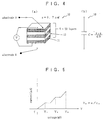
- FIG. 4 shows a structure and an equivalent circuit diagram of a single electron tunneling transistor of the first embodiment of the present invention.
- reference numeral 10 denotes a single electron tunneling transistor
- reference numeral 11 denotes an electrically conductive layer (CuO 2 )
- reference numeral 12 denotes a tunneling barrier layer (BiO).
- FIG. 5 shows I-V characteristics of the single electron tunneling transistor of the first embodiment of the present invention, in which the axis of abscissa represents voltage (mV) and the axis of ordinate represents current ( ⁇ A).
- FIG. 6 shows a structure and the equivalent circuit diagram of a single electron tunneling transistor of the second embodiment of the present invention, in which V G represents gate voltage.
- FIG. 6(a) shows a single electron tunneling transistor 21 having a control gate G.
- the gate G is connected, through a gate capacitance C G , to a series single electron tunneling element which has capacitances C A and C B .
- FIG. 7 shows I-V characteristics of the single electron tunneling transistor of the second embodiment of the present invention, in which the axis of abscissa represents voltage (mV) and the axis of ordinate represents current ( ⁇ A).
- control gate G as shown in FIG. 6 is not necessarily easy.
- a multi-layer tunneling material formed of a multi-layer single crystal or an artificial multi-layer structure is processed to provide grooves (a-1 through a-4) as shown in FIG. 8, and current is allowed to flow from terminal A to terminal B.
- the current flows through the tunneling element between grooves a-1 and a-2, and then through the tunneling element between grooves a-3 and a-4 to terminal B.
- the present invention is suitably applicable to a superconductive single-crystal single-electron transistor and a memory for LSIs. Moreover, the present invention is applicable not only to high temperature superconductive materials, but also to a high-temperature-operating single electron tunneling transistor formed from a material of thin film or a single crystal of multi-layer structure.
Landscapes
- Engineering & Computer Science (AREA)
- Chemical & Material Sciences (AREA)
- Nanotechnology (AREA)
- Physics & Mathematics (AREA)
- Mathematical Physics (AREA)
- Theoretical Computer Science (AREA)
- Crystallography & Structural Chemistry (AREA)
- Superconductor Devices And Manufacturing Methods Thereof (AREA)
- Bipolar Transistors (AREA)
Abstract
Description
Claims (3)
- A single electron tunneling transistor having a multi-layer structure, comprising a plurality of electrically conductive layers and a plurality of tunneling barrier layers, the conductive layers and the tunneling barrier layers being alternately stacked one on another, the total number of the conductive layers and the tunneling barrier layers being at least 50, and a minute tunneling junction in the structure having an area on the order of 1 µm square.
- A single electron tunneling transistor having a multi-layer structure, comprising a plurality of electrically conductive layers and a plurality of tunneling barrier layers, the conductive layers and the tunneling barrier layers being alternately stacked one on another, and a control gate, the total number of the conductive layers and the tunneling barrier layers being at least 50, and a minute tunneling junction in the structure having an area on the order of 1 µm square.
- A single electron tunneling transistor having a multi-layer structure as described in claim 2, wherein the control gate is formed at a central portion of the single electron tunneling transistor, a first and a second pairs of grooves being provided centering the control gate, the grooves of each pair opening toward opposite directions, so as to permit an electric field to be applied to bottom portions of the grooves provided centering the control gate.
Applications Claiming Priority (3)
| Application Number | Priority Date | Filing Date | Title |
|---|---|---|---|
| JP19922199 | 1999-07-13 | ||
| JP19922199A JP3231742B2 (en) | 1999-07-13 | 1999-07-13 | Single-electron tunnel transistor using stacked structure |
| PCT/JP2000/004621 WO2001004959A1 (en) | 1999-07-13 | 2000-07-11 | Single electron tunneling transistor having multilayer structure |
Publications (2)
| Publication Number | Publication Date |
|---|---|
| EP1205979A1 true EP1205979A1 (en) | 2002-05-15 |
| EP1205979A4 EP1205979A4 (en) | 2007-05-30 |
Family
ID=16404167
Family Applications (1)
| Application Number | Title | Priority Date | Filing Date |
|---|---|---|---|
| EP00944394A Withdrawn EP1205979A4 (en) | 1999-07-13 | 2000-07-11 | TRANSISTOR WITH A MULTILAYER STRUCTURE CHANNELING A SINGLE ELECTRON |
Country Status (4)
| Country | Link |
|---|---|
| US (1) | US6573526B1 (en) |
| EP (1) | EP1205979A4 (en) |
| JP (1) | JP3231742B2 (en) |
| WO (1) | WO2001004959A1 (en) |
Families Citing this family (8)
| Publication number | Priority date | Publication date | Assignee | Title |
|---|---|---|---|---|
| JP4906173B2 (en) * | 1999-12-07 | 2012-03-28 | 克幸 津久井 | Switching device without insulator barrier using superlattice |
| US7026642B2 (en) * | 2003-08-27 | 2006-04-11 | Micron Technology, Inc. | Vertical tunneling transistor |
| US6946693B1 (en) | 2004-04-27 | 2005-09-20 | Wisconsin Alumni Research Foundation | Electromechanical electron transfer devices |
| KR101119851B1 (en) * | 2004-09-09 | 2012-03-16 | 국립대학법인 홋가이도 다이가쿠 | Function element, storage element, magnetic recording element, solar cell, photoelectric conversion element, light emitting element, catalyst reaction device, and clean unit |
| CN100505356C (en) * | 2006-03-07 | 2009-06-24 | 中国科学院物理研究所 | Closed superconductive loop multi-layer film, its making method and use |
| US8824190B1 (en) * | 2013-03-05 | 2014-09-02 | International Business Machines Corporation | Memory state sensing based on cell capacitance |
| US10381468B2 (en) | 2017-03-21 | 2019-08-13 | International Business Machines Corporation | Method and structure for forming improved single electron transistor with gap tunnel barriers |
| CN107579112B (en) * | 2017-08-09 | 2018-11-16 | 北京梦之墨科技有限公司 | A kind of full liquid quantum tunneling effect device and preparation method thereof |
Family Cites Families (4)
| Publication number | Priority date | Publication date | Assignee | Title |
|---|---|---|---|---|
| JP3500541B2 (en) * | 1994-02-15 | 2004-02-23 | 富士通株式会社 | Manufacturing method of single electron tunnel junction device |
| JPH09139491A (en) | 1995-11-13 | 1997-05-27 | Fujitsu Ltd | Single electron semiconductor device and manufacturing method thereof |
| US6117711A (en) * | 1998-03-02 | 2000-09-12 | Texas Instruments - Acer Incorporated | Method of making single-electron-tunneling CMOS transistors |
| JP4027504B2 (en) * | 1998-07-27 | 2007-12-26 | 独立行政法人科学技術振興機構 | Single-electron tunnel device having a laminated structure and manufacturing method thereof |
-
1999
- 1999-07-13 JP JP19922199A patent/JP3231742B2/en not_active Expired - Fee Related
-
2000
- 2000-07-11 EP EP00944394A patent/EP1205979A4/en not_active Withdrawn
- 2000-07-11 US US10/019,430 patent/US6573526B1/en not_active Expired - Fee Related
- 2000-07-11 WO PCT/JP2000/004621 patent/WO2001004959A1/en not_active Ceased
Also Published As
| Publication number | Publication date |
|---|---|
| WO2001004959A1 (en) | 2001-01-18 |
| US6573526B1 (en) | 2003-06-03 |
| EP1205979A4 (en) | 2007-05-30 |
| JP3231742B2 (en) | 2001-11-26 |
| JP2001024244A (en) | 2001-01-26 |
Similar Documents
| Publication | Publication Date | Title |
|---|---|---|
| EP0494580B1 (en) | Superconducting field-effect transistor with inverted MISFET structure and method for making the same | |
| US6573526B1 (en) | Single electron tunneling transistor having multilayer structure | |
| US6734454B2 (en) | Internally shunted Josephson junction device | |
| JP4027504B2 (en) | Single-electron tunnel device having a laminated structure and manufacturing method thereof | |
| JP3995810B2 (en) | High temperature single electron pair tunneling device manufacturing method using layered oxide superconductor | |
| US5856205A (en) | Josephson junction device of oxide superconductor having low noise level at liquid nitrogen temperature | |
| JPH0783144B2 (en) | Jyosefson device using oxide superconductor | |
| JP2829201B2 (en) | Superconducting element | |
| JP2730502B2 (en) | Superconducting transistor | |
| KR100267974B1 (en) | method for fabricating josephson junction device operating on high temperature | |
| JP2907094B2 (en) | Superconducting transistor | |
| JPH0555648A (en) | Superconducting element | |
| JPH05291637A (en) | Superconductive field effect type element | |
| JPH09312424A (en) | Superconducting transistor | |
| JPH065937A (en) | Non-linear characteristic element | |
| Takayasu et al. | Negative-resistance voltage-current characteristics of superconductor contact junctions for macro-scale applications | |
| JPH05152629A (en) | Superconducting field effect element and method of manufacturing the same | |
| JPS63248187A (en) | superconducting device | |
| JPH02244682A (en) | Superconductive element | |
| JPH0537033A (en) | Superconductive device | |
| JPH0613667A (en) | Superconducting field effect device and method of manufacturing the same | |
| JPH0283986A (en) | Superconducting diode | |
| JPH07240541A (en) | Superconducting 3-terminal element | |
| JPH0256978A (en) | superconducting element | |
| JPH08162682A (en) | Superconducting device and manufacturing method thereof |
Legal Events
| Date | Code | Title | Description |
|---|---|---|---|
| PUAI | Public reference made under article 153(3) epc to a published international application that has entered the european phase |
Free format text: ORIGINAL CODE: 0009012 |
|
| 17P | Request for examination filed |
Effective date: 20020111 |
|
| AK | Designated contracting states |
Kind code of ref document: A1 Designated state(s): AT BE CH CY DE DK ES FI FR GB GR IE IT LI LU MC NL PT SE |
|
| RBV | Designated contracting states (corrected) |
Designated state(s): DE FR GB |
|
| RAP1 | Party data changed (applicant data changed or rights of an application transferred) |
Owner name: JAPAN SCIENCE AND TECHNOLOGY AGENCY |
|
| RAP1 | Party data changed (applicant data changed or rights of an application transferred) |
Owner name: JAPAN SCIENCE AND TECHNOLOGY AGENCY |
|
| A4 | Supplementary search report drawn up and despatched |
Effective date: 20070503 |
|
| 17Q | First examination report despatched |
Effective date: 20080612 |
|
| GRAP | Despatch of communication of intention to grant a patent |
Free format text: ORIGINAL CODE: EPIDOSNIGR1 |
|
| STAA | Information on the status of an ep patent application or granted ep patent |
Free format text: STATUS: THE APPLICATION IS DEEMED TO BE WITHDRAWN |
|
| 18D | Application deemed to be withdrawn |
Effective date: 20110826 |