EP1205966A2 - Method for improving the uniformity and reducing the roughness of a silicon surface before dielectric layer formation - Google Patents
Method for improving the uniformity and reducing the roughness of a silicon surface before dielectric layer formation Download PDFInfo
- Publication number
- EP1205966A2 EP1205966A2 EP01000615A EP01000615A EP1205966A2 EP 1205966 A2 EP1205966 A2 EP 1205966A2 EP 01000615 A EP01000615 A EP 01000615A EP 01000615 A EP01000615 A EP 01000615A EP 1205966 A2 EP1205966 A2 EP 1205966A2
- Authority
- EP
- European Patent Office
- Prior art keywords
- dielectric layer
- silicon
- forming
- amorphous region
- species
- Prior art date
- Legal status (The legal status is an assumption and is not a legal conclusion. Google has not performed a legal analysis and makes no representation as to the accuracy of the status listed.)
- Withdrawn
Links
Images


Classifications
-
- H—ELECTRICITY
- H10—SEMICONDUCTOR DEVICES; ELECTRIC SOLID-STATE DEVICES NOT OTHERWISE PROVIDED FOR
- H10P—GENERIC PROCESSES OR APPARATUS FOR THE MANUFACTURE OR TREATMENT OF DEVICES COVERED BY CLASS H10
- H10P70/00—Cleaning of wafers, substrates or parts of devices
- H10P70/10—Cleaning before device manufacture, i.e. Begin-Of-Line process
- H10P70/12—Cleaning before device manufacture, i.e. Begin-Of-Line process by dry cleaning only
-
- H—ELECTRICITY
- H10—SEMICONDUCTOR DEVICES; ELECTRIC SOLID-STATE DEVICES NOT OTHERWISE PROVIDED FOR
- H10D—INORGANIC ELECTRIC SEMICONDUCTOR DEVICES
- H10D64/00—Electrodes of devices having potential barriers
- H10D64/01—Manufacture or treatment
- H10D64/013—Manufacture or treatment of electrodes having a conductor capacitively coupled to a semiconductor by an insulator
- H10D64/01302—Manufacture or treatment of electrodes having a conductor capacitively coupled to a semiconductor by an insulator the insulator being formed after the semiconductor body, the semiconductor being silicon
- H10D64/01332—Making the insulator
- H10D64/01336—Making the insulator on single crystalline silicon, e.g. chemical oxidation using a liquid
-
- H—ELECTRICITY
- H10—SEMICONDUCTOR DEVICES; ELECTRIC SOLID-STATE DEVICES NOT OTHERWISE PROVIDED FOR
- H10D—INORGANIC ELECTRIC SEMICONDUCTOR DEVICES
- H10D64/00—Electrodes of devices having potential barriers
- H10D64/01—Manufacture or treatment
- H10D64/013—Manufacture or treatment of electrodes having a conductor capacitively coupled to a semiconductor by an insulator
- H10D64/01302—Manufacture or treatment of electrodes having a conductor capacitively coupled to a semiconductor by an insulator the insulator being formed after the semiconductor body, the semiconductor being silicon
- H10D64/01332—Making the insulator
- H10D64/01348—Making the insulator with substrate doping, e.g. N, Ge or C implantation, before formation of the insulator
-
- H—ELECTRICITY
- H10—SEMICONDUCTOR DEVICES; ELECTRIC SOLID-STATE DEVICES NOT OTHERWISE PROVIDED FOR
- H10P—GENERIC PROCESSES OR APPARATUS FOR THE MANUFACTURE OR TREATMENT OF DEVICES COVERED BY CLASS H10
- H10P14/00—Formation of materials, e.g. in the shape of layers or pillars
- H10P14/60—Formation of materials, e.g. in the shape of layers or pillars of insulating materials
- H10P14/65—Formation of materials, e.g. in the shape of layers or pillars of insulating materials characterised by treatments performed before or after the formation of the materials
- H10P14/6502—Formation of materials, e.g. in the shape of layers or pillars of insulating materials characterised by treatments performed before or after the formation of the materials of treatments performed before formation of the materials
- H10P14/6512—Formation of materials, e.g. in the shape of layers or pillars of insulating materials characterised by treatments performed before or after the formation of the materials of treatments performed before formation of the materials by exposure to a gas or vapour
-
- H—ELECTRICITY
- H10—SEMICONDUCTOR DEVICES; ELECTRIC SOLID-STATE DEVICES NOT OTHERWISE PROVIDED FOR
- H10P—GENERIC PROCESSES OR APPARATUS FOR THE MANUFACTURE OR TREATMENT OF DEVICES COVERED BY CLASS H10
- H10P50/00—Etching of wafers, substrates or parts of devices
-
- H—ELECTRICITY
- H10—SEMICONDUCTOR DEVICES; ELECTRIC SOLID-STATE DEVICES NOT OTHERWISE PROVIDED FOR
- H10D—INORGANIC ELECTRIC SEMICONDUCTOR DEVICES
- H10D64/00—Electrodes of devices having potential barriers
- H10D64/01—Manufacture or treatment
- H10D64/013—Manufacture or treatment of electrodes having a conductor capacitively coupled to a semiconductor by an insulator
- H10D64/01302—Manufacture or treatment of electrodes having a conductor capacitively coupled to a semiconductor by an insulator the insulator being formed after the semiconductor body, the semiconductor being silicon
- H10D64/01332—Making the insulator
- H10D64/01336—Making the insulator on single crystalline silicon, e.g. chemical oxidation using a liquid
- H10D64/01342—Making the insulator on single crystalline silicon, e.g. chemical oxidation using a liquid by deposition, e.g. evaporation, ALD or laser deposition
-
- H—ELECTRICITY
- H10—SEMICONDUCTOR DEVICES; ELECTRIC SOLID-STATE DEVICES NOT OTHERWISE PROVIDED FOR
- H10D—INORGANIC ELECTRIC SEMICONDUCTOR DEVICES
- H10D64/00—Electrodes of devices having potential barriers
- H10D64/60—Electrodes characterised by their materials
- H10D64/66—Electrodes having a conductor capacitively coupled to a semiconductor by an insulator, e.g. MIS electrodes
- H10D64/68—Electrodes having a conductor capacitively coupled to a semiconductor by an insulator, e.g. MIS electrodes characterised by the insulator, e.g. by the gate insulator
- H10D64/693—Electrodes having a conductor capacitively coupled to a semiconductor by an insulator, e.g. MIS electrodes characterised by the insulator, e.g. by the gate insulator the insulator comprising nitrogen, e.g. nitrides, oxynitrides or nitrogen-doped materials
-
- H—ELECTRICITY
- H10—SEMICONDUCTOR DEVICES; ELECTRIC SOLID-STATE DEVICES NOT OTHERWISE PROVIDED FOR
- H10P—GENERIC PROCESSES OR APPARATUS FOR THE MANUFACTURE OR TREATMENT OF DEVICES COVERED BY CLASS H10
- H10P14/00—Formation of materials, e.g. in the shape of layers or pillars
- H10P14/60—Formation of materials, e.g. in the shape of layers or pillars of insulating materials
- H10P14/69—Inorganic materials
- H10P14/692—Inorganic materials composed of oxides, glassy oxides or oxide-based glasses
- H10P14/6921—Inorganic materials composed of oxides, glassy oxides or oxide-based glasses containing silicon
- H10P14/69215—Inorganic materials composed of oxides, glassy oxides or oxide-based glasses containing silicon the material being a silicon oxide, e.g. SiO2
-
- H—ELECTRICITY
- H10—SEMICONDUCTOR DEVICES; ELECTRIC SOLID-STATE DEVICES NOT OTHERWISE PROVIDED FOR
- H10P—GENERIC PROCESSES OR APPARATUS FOR THE MANUFACTURE OR TREATMENT OF DEVICES COVERED BY CLASS H10
- H10P14/00—Formation of materials, e.g. in the shape of layers or pillars
- H10P14/60—Formation of materials, e.g. in the shape of layers or pillars of insulating materials
- H10P14/69—Inorganic materials
- H10P14/694—Inorganic materials composed of nitrides
- H10P14/6943—Inorganic materials composed of nitrides containing silicon
- H10P14/69433—Inorganic materials composed of nitrides containing silicon the material being a silicon nitride not containing oxygen, e.g. SixNy or SixByNz
Definitions
- the present invention relates to a method to improve the uniformity and reduce the surface roughness of the silicon surface at a silicon and silicon oxide interface.
- the thickness of the gate oxide has been reduced to less than 2nm. In this thickness regime, surface roughness and non-uniformity have a significant impact on device performance.
- Shown in Figure 1 is a typical MOS transistor. As described above, the thickness of the gate dielectric 20 can be less than 2nm.
- the gate dielectric 20 will comprise silicon oxide formed on the silicon substrate.
- the gate electrode 30, the sidewall structures 40, and the drain region 50 and the source region 60 also comprise the MOS transistor.
- the MOS transistor shown in Figure 1 can be formed using standard well known processing techniques. In operation, the proper voltages are applied to the gate 30, drain 50, source 60, and substrate regions 10 to form a depletion region 70 and an inversion region 80.
- the inversion region 80 is formed at the silicon substrate/gate dielectric interface 90 and comprises free carriers. It is the motion of these free carriers in the inversion region 80 from the source 60 to the drain 50 which results in the drain/source current of the transistor. The amount of transistor current which is produced for given applied voltages depends on the rate at which these free carriers flow through the inversion region 80.
- FIG 2 Shown in Figure 2 is a magnified view of the silicon substrate/gate dielectric region for section 100 illustrate in Figure 1.
- the silicon substrate/gate dielectric interface 90 is not smooth but instead comprises surface roughness shown here in the form of steps.
- the free carriers in the inversion 110 collide with these steps (or surface roughness) in flowing through the inversion region. These collisions impede the flow of carriers 110 and thus reduce the transistor current. These collisions are enhanced in the case of thin gate dielectrics (i.e. less than 2nm) due to the high electric fields that exist in the inversion layer 80 which forces the free carriers 110 against the interface 90.
- the presence of the surface roughness introduces non-uniformities in the thickness of the gate dielectric layer 20. These non-uniformities are becoming increasingly important as the thickness of the gate dielectric layer is reduced.
- the instant invention is a method for forming an atomically smooth interface between a silicon substrate and a dielectric layer.
- a thin amorphous region is formed on the surface of the silicon substrate.
- the dielectric layer can be formed using known techniques of thermal growth or film deposition.
- the method comprises: providing a silicon substrate with an upper surface; forming an amorphous region in said upper surface by exposing said upper surface to halogen species; and forming a dielectric layer on said amorphous region.
- the instant invention comprises forming an amorphous region at the silicon surface before formation of a dielectric layer.
- the formation of the amorphous region eliminates the surface roughness shown in Figure 2.
- the method of amorphous region formation comprises exposing the bare silicon surface to halogen species. The method will be described with reference to a MOS transistor. It should however be noted that the method applies to the formation of a smooth interface between the surface of a silicon substrate and a dielectric layer which can be used in any semiconductor device requiring such an interface.
- Shown in Figure 3 is a flow diagram outlining the method of the instant invention.
- a number of known processing steps are performed before the dielectric layer which will comprise the gate of the MOS transistor is formed. These processing steps include, but are not limited to, isolation formation, n-well formation and p-well formation.
- Shown in Figure 4 is a cross-section diagram of a silicon substrate 10 containing dielectric isolation structures 140 and various n-well regions 150 and p-well regions 160 on which the gate dielectric layer will be formed.
- the first step in the method of the instant invention is the removal of any thin dielectric layers from the silicon substrate surface 170. In most instances this thin dielectric layer will comprise silicon oxide.
- the thin dielectric film can be removed using wet or dry methods.
- the silicon oxide film can be removed using a dilute HF solution.
- a dilute HF solution can comprise a 1:100 volume dilution of 49% HF at room temperature for a duration that is adequate to completely remove the silicon oxide layer.
- a dry process comprising a mixture of anhydrous HF and isopropyl-alcohol can be used to remove the silicon oxide layer.
- a thin amorphous region is formed at the surface as outlined in 120 of Figure 3 and shown in Figure 5.
- the thin amorphous region 180 illustrated in Figure 5 is formed by exposing the silicon substrate surface 170 to halogen species.
- the halogen atoms or molecules are in an energetic excited state and/or the surface 170 of the silicon substrate is heated.
- ultra violet (UV) radiation is used to generate excited chlorine (Cl) species using chlorine containing gases.
- Excited chlorine species in the instant invention refers to chlorine species where some of the electrons associated with the chlorine species occupy higher energy states after expose to the UV radiation.
- UV radiation can also be used to heat the surface of the silicon substrate 170 to the temperature range of 50°C to 250°C depending on the degree of amorphization desired.
- the flow of the chlorine containing gas can be varied in the range of 150sccm to 600sccm with a typical value of 350sccm.
- the pressure in the process chamber can be set between ltorr and 25torr with a typical value of 6torr.
- the amorphous region 180 created using the above method is self limiting with a typical layer thickness of a few angstroms. Formation of the amorphous layer 180 will eliminate the surface roughness shown in Figure 2 allowing for improved gate dielectric layer thickness uniformity.
- halogen species can be used to form the amorphous region. These species include bromine, iodine and fluorine.
- any suitable method of producing excited halogen species can be used. Such methods may include plasma and microwave excitation.
- the wafer surface can be heated using any number of suitable methods in addition to the UV method described above. Such methods might include contact heating implemented by heating the wafer holder.
- a) thin dielectric layer removal, b)amorphous layer formation, and c) the subsequent oxide and/or dielectric layer formation can be performed in a controlled ambient.
- the dielectric layer can be formed without exposing the amorphous region to an oxidizing ambient such as would be the case if the wafer had to be transported from process tool to process tool in the ambient of a silicon fabrication facility.
- a optional protective silicon oxide cap can be formed on the amorphous layer 180 using a low temperature self-limiting process.
- This optional step 125 is illustrated in Figure 3.
- UV radiation can be used in conjunction with an oxygen containing gas mixture to grow about 6A of silicon oxide by a self-limiting process. In an embodiment of the instant invention this comprises oxygen gas.
- the formation of this protective silicon oxide capping layer is an optional step. Whether or not this protective capping layer is formed will depend on a number of factors including whether a cluster type processing tool is used.
- the dielectric layer is formed 190 as shown in Figure 6.
- This dielectric layer formation step 130 is illustrated in Figure 3.
- the dielectric layer 190 can be formed using thermal growth or film deposition methods.
- the silicon oxide layer can be formed by heating the surface of the silicon substrate containing the amorphous region and exposing the heated surface to an oxidizing ambient containing oxygen species.
- a number of well known methods for forming silicon oxide dielectric layers using thermal oxidation methods exist in the art.
- the MOS transistor (or any other device) can be completed using known processing methods.
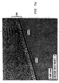
- Shown in Figure 7(a) is a TEM micrographs showing the silicon/silicon oxide interface for a silicon surface that was prepared using existing methods.
- the interface region 200 shows visible surface roughness.
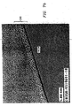
- Shown in Figure 7(b) is a TEM micrographs showing the silicon/silicon oxide interface for a silicon surface that was prepared using the method of the instant invention. In particular, an amorphous region was formed at the surface using UV excited chlorine containing gas before the oxidation process.
- the interface region 210 shows a sharply defined transition region with no visible signs of surface roughness.
- a gate dielectric layer of silicon oxide can be deposited on the amorphous region using known deposition methods.
- other suitable gate dielectric layers include silicon nitride, silicon oxynitride, and high dielectric constant films like silicates can be used.
- the instant invention has been described with reference to a MOS transistor.
- the method is not however confined to a MOS transistor.
- the method can be used to form an atomically smooth silicon/dielectric interface in any number of other semiconductor devices including MOS capacitors, memory cells, detectors, charge coupled devices, thin film transistors, etc.
Landscapes
- Insulated Gate Type Field-Effect Transistor (AREA)
- Formation Of Insulating Films (AREA)
- Recrystallisation Techniques (AREA)
Abstract
Description
Claims (9)
- A method for forming an interface between a silicon surface and a dielectric layer comprising:providing a silicon substrate with an upper surface;forming an amorphous region in said upper surface by exposing said upper surface to halogen species; andforming a dielectric layer over said amorphous region.
- The method of claim 1 further comprising removing a thin dielectric layer from said upper surface prior to forming said amorphous region.
- The method of claim 1 or claim 2 wherein said forming said amorphous further comprises:exposing a chlorine containing gas to UV radiation to form excited chlorine species;heating said upper surface to a temperature between 50oC and 250oC; andexposing said heated upper surface to said excited chlorine species.
- The method of any preceding claim wherein said dielectric layer is formed using a material selected from the group consisting of silicon oxide, silicon nitride, silicon oxynitride, and a silicate.
- The method as claimed in any preceding claim and further comprising:forming a capping layer intermediate said amorphous region and said dielectric layer.
- The method of any preceding claim further comprising removing a thin dielectric layer from said upper surface prior to forming said amorphous region.
- The method of any preceding claim wherein said halogen species is selected from the group consisting of chlorine, bromine, iodine and fluorine.
- The method of any preceding claim wherein said forming said amorphous further comprises:exposing a chlorine containing gas to UV radiation to form excited chlorine species;heating said upper surface to a temperature between 50°C and 250°C; andexposing said heated upper surface to said excited chlorine species.
- The method of any preceding claim wherein said dielectric layer is formed using a material selected from the group consisting of silicon oxide, silicon nitride, silicon oxynitride, and a silicate.
Applications Claiming Priority (2)
| Application Number | Priority Date | Filing Date | Title |
|---|---|---|---|
| US24740800P | 2000-11-10 | 2000-11-10 | |
| US247408P | 2000-11-10 |
Publications (2)
| Publication Number | Publication Date |
|---|---|
| EP1205966A2 true EP1205966A2 (en) | 2002-05-15 |
| EP1205966A3 EP1205966A3 (en) | 2006-03-29 |
Family
ID=22934810
Family Applications (1)
| Application Number | Title | Priority Date | Filing Date |
|---|---|---|---|
| EP01000615A Withdrawn EP1205966A3 (en) | 2000-11-10 | 2001-11-09 | Method for improving the uniformity and reducing the roughness of a silicon surface before dielectric layer formation |
Country Status (5)
| Country | Link |
|---|---|
| US (1) | US6939816B2 (en) |
| EP (1) | EP1205966A3 (en) |
| JP (1) | JP2002222810A (en) |
| CN (1) | CN1212641C (en) |
| TW (1) | TW516172B (en) |
Families Citing this family (6)
| Publication number | Priority date | Publication date | Assignee | Title |
|---|---|---|---|---|
| US6747318B1 (en) * | 2001-12-13 | 2004-06-08 | Lsi Logic Corporation | Buried channel devices and a process for their fabrication simultaneously with surface channel devices to produce transistors and capacitors with multiple electrical gate oxides |
| US6762114B1 (en) | 2002-12-31 | 2004-07-13 | Texas Instruments Incorporated | Methods for transistor gate fabrication and for reducing high-k gate dielectric roughness |
| US6750126B1 (en) | 2003-01-08 | 2004-06-15 | Texas Instruments Incorporated | Methods for sputter deposition of high-k dielectric films |
| EP2058844A1 (en) * | 2007-10-30 | 2009-05-13 | Interuniversitair Microelektronica Centrum (IMEC) | Method of forming a semiconductor device |
| CN102420122B (en) * | 2011-06-07 | 2013-10-02 | 上海华力微电子有限公司 | Method used for enhancing tensile stress of silicon nitride film |
| US11575006B2 (en) | 2018-03-20 | 2023-02-07 | The Regents Of The University Of California | Van der Waals integration approach for material integration and device fabrication |
Family Cites Families (14)
| Publication number | Priority date | Publication date | Assignee | Title |
|---|---|---|---|---|
| US4140548A (en) * | 1978-05-19 | 1979-02-20 | Maruman Integrated Circuits Inc. | MOS Semiconductor process utilizing a two-layer oxide forming technique |
| JPS62272540A (en) * | 1986-05-20 | 1987-11-26 | Fujitsu Ltd | Manufacture of semiconductor |
| US5178682A (en) * | 1988-06-21 | 1993-01-12 | Mitsubishi Denki Kabushiki Kaisha | Method for forming a thin layer on a semiconductor substrate and apparatus therefor |
| JPH0697101A (en) * | 1992-09-11 | 1994-04-08 | Ricoh Co Ltd | Method of manufacturing thin film transistor element |
| US5445999A (en) * | 1992-11-13 | 1995-08-29 | Micron Technology, Inc. | Advanced technique to improve the bonding arrangement on silicon surfaces to promote uniform nitridation |
| CN1156918C (en) * | 1993-12-02 | 2004-07-07 | 株式会社半导体能源研究所 | Semiconductor device |
| US6083849A (en) * | 1995-11-13 | 2000-07-04 | Micron Technology, Inc. | Methods of forming hemispherical grain polysilicon |
| US5953591A (en) * | 1995-12-28 | 1999-09-14 | Nippon Sanso Corporation | Process for laser detection of gas and contaminants in a wafer transport gas tunnel |
| US6287988B1 (en) * | 1997-03-18 | 2001-09-11 | Kabushiki Kaisha Toshiba | Semiconductor device manufacturing method, semiconductor device manufacturing apparatus and semiconductor device |
| JP3844566B2 (en) * | 1997-07-30 | 2006-11-15 | 株式会社半導体エネルギー研究所 | Method for manufacturing semiconductor device |
| US6475815B1 (en) * | 1998-12-09 | 2002-11-05 | Matsushita Electric Industrial Co., Ltd. | Method of measuring temperature, method of taking samples for temperature measurement and method for fabricating semiconductor device |
| JP2000349081A (en) * | 1999-06-07 | 2000-12-15 | Sony Corp | Oxide film formation method |
| KR20010003691A (en) * | 1999-06-24 | 2001-01-15 | 김영환 | Method of forming shallow junction of semiconductor device |
| JP3579316B2 (en) * | 1999-10-19 | 2004-10-20 | 三洋電機株式会社 | Method for manufacturing semiconductor device |
-
2001
- 2001-11-01 US US10/001,483 patent/US6939816B2/en not_active Expired - Lifetime
- 2001-11-09 TW TW090127876A patent/TW516172B/en not_active IP Right Cessation
- 2001-11-09 CN CNB011374209A patent/CN1212641C/en not_active Expired - Fee Related
- 2001-11-09 JP JP2001344028A patent/JP2002222810A/en active Pending
- 2001-11-09 EP EP01000615A patent/EP1205966A3/en not_active Withdrawn
Also Published As
| Publication number | Publication date |
|---|---|
| TW516172B (en) | 2003-01-01 |
| US6939816B2 (en) | 2005-09-06 |
| US20020058424A1 (en) | 2002-05-16 |
| EP1205966A3 (en) | 2006-03-29 |
| CN1212641C (en) | 2005-07-27 |
| CN1357906A (en) | 2002-07-10 |
| JP2002222810A (en) | 2002-08-09 |
Similar Documents
| Publication | Publication Date | Title |
|---|---|---|
| TWI553734B (en) | Method for low temperature oxidation of semiconductor components | |
| EP1923910B1 (en) | Selective removal of rare earth comprising materials in a semiconductor device | |
| US9093389B2 (en) | Method of patterning a silicon nitride dielectric film | |
| US6953727B2 (en) | Manufacture method of semiconductor device with gate insulating films of different thickness | |
| JP2002261097A (en) | Dielectric film and method of forming the same, semiconductor device, nonvolatile semiconductor memory device, and method of manufacturing semiconductor device | |
| JP3746478B2 (en) | Manufacturing method of semiconductor device | |
| CN101620995A (en) | Gate dielectric layer, manufacturing method thereof, semiconductor device and manufacturing method thereof | |
| US20040102010A1 (en) | Reliable high voltage gate dielectric layers using a dual nitridation process | |
| US7157339B2 (en) | Method for fabricating semiconductor devices having dual gate oxide layers | |
| US7378335B2 (en) | Plasma implantation of deuterium for passivation of semiconductor-device interfaces | |
| US6939816B2 (en) | Method to improve the uniformity and reduce the surface roughness of the silicon dielectric interface | |
| US8822349B1 (en) | Oxide formation in a plasma process | |
| US20060205192A1 (en) | Shallow-junction fabrication in semiconductor devices via plasma implantation and deposition | |
| US9570582B1 (en) | Method of removing dummy gate dielectric layer | |
| US6117711A (en) | Method of making single-electron-tunneling CMOS transistors | |
| US6579766B1 (en) | Dual gate oxide process without critical resist and without N2 implant | |
| US6358798B1 (en) | Method for forming gate electrode by damascene process | |
| TWI411009B (en) | Dielectric film and method of forming same | |
| CN100459053C (en) | Method for manufacturing gate structure of semiconductor device | |
| JP3578345B2 (en) | Semiconductor device manufacturing method and semiconductor device | |
| JP2005079563A (en) | Manufacturing method of electronic device | |
| EP0911869A2 (en) | Low temperature method for forming a uniform thin oxide layer | |
| US8748260B2 (en) | Method for manufacturing nano-crystalline silicon material for semiconductor integrated circuits | |
| JP2002343965A (en) | MIS type semiconductor device and method of manufacturing the same | |
| US6897112B2 (en) | Method for fabricating an integrated semiconductor configuration with the aid of thermal oxidation, related semiconductor configuration, and related memory unit |
Legal Events
| Date | Code | Title | Description |
|---|---|---|---|
| PUAI | Public reference made under article 153(3) epc to a published international application that has entered the european phase |
Free format text: ORIGINAL CODE: 0009012 |
|
| AK | Designated contracting states |
Kind code of ref document: A2 Designated state(s): AT BE CH CY DE DK ES FI FR GB GR IE IT LI LU MC NL PT SE TR |
|
| AX | Request for extension of the european patent |
Free format text: AL;LT;LV;MK;RO;SI |
|
| PUAL | Search report despatched |
Free format text: ORIGINAL CODE: 0009013 |
|
| AK | Designated contracting states |
Kind code of ref document: A3 Designated state(s): AT BE CH CY DE DK ES FI FR GB GR IE IT LI LU MC NL PT SE TR |
|
| AX | Request for extension of the european patent |
Extension state: AL LT LV MK RO SI |
|
| AKX | Designation fees paid | ||
| REG | Reference to a national code |
Ref country code: DE Ref legal event code: 8566 |
|
| STAA | Information on the status of an ep patent application or granted ep patent |
Free format text: STATUS: THE APPLICATION IS DEEMED TO BE WITHDRAWN |
|
| 18D | Application deemed to be withdrawn |
Effective date: 20061004 |