EP1205575A1 - Method for producing ceramic and apparatus for producing the same, semiconductor device, and piezoelectric device - Google Patents
Method for producing ceramic and apparatus for producing the same, semiconductor device, and piezoelectric device Download PDFInfo
- Publication number
- EP1205575A1 EP1205575A1 EP01917596A EP01917596A EP1205575A1 EP 1205575 A1 EP1205575 A1 EP 1205575A1 EP 01917596 A EP01917596 A EP 01917596A EP 01917596 A EP01917596 A EP 01917596A EP 1205575 A1 EP1205575 A1 EP 1205575A1
- Authority
- EP
- European Patent Office
- Prior art keywords
- ceramics
- film
- ceramic film
- fabricating
- active species
- Prior art date
- Legal status (The legal status is an assumption and is not a legal conclusion. Google has not performed a legal analysis and makes no representation as to the accuracy of the status listed.)
- Withdrawn
Links
Images




Classifications
-
- C—CHEMISTRY; METALLURGY
- C23—COATING METALLIC MATERIAL; COATING MATERIAL WITH METALLIC MATERIAL; CHEMICAL SURFACE TREATMENT; DIFFUSION TREATMENT OF METALLIC MATERIAL; COATING BY VACUUM EVAPORATION, BY SPUTTERING, BY ION IMPLANTATION OR BY CHEMICAL VAPOUR DEPOSITION, IN GENERAL; INHIBITING CORROSION OF METALLIC MATERIAL OR INCRUSTATION IN GENERAL
- C23C—COATING METALLIC MATERIAL; COATING MATERIAL WITH METALLIC MATERIAL; SURFACE TREATMENT OF METALLIC MATERIAL BY DIFFUSION INTO THE SURFACE, BY CHEMICAL CONVERSION OR SUBSTITUTION; COATING BY VACUUM EVAPORATION, BY SPUTTERING, BY ION IMPLANTATION OR BY CHEMICAL VAPOUR DEPOSITION, IN GENERAL
- C23C16/00—Chemical coating by decomposition of gaseous compounds, without leaving reaction products of surface material in the coating, i.e. chemical vapour deposition [CVD] processes
- C23C16/22—Chemical coating by decomposition of gaseous compounds, without leaving reaction products of surface material in the coating, i.e. chemical vapour deposition [CVD] processes characterised by the deposition of inorganic material, other than metallic material
- C23C16/30—Deposition of compounds, mixtures or solid solutions, e.g. borides, carbides, nitrides
- C23C16/40—Oxides
- C23C16/409—Oxides of the type ABO3 with A representing alkali, alkaline earth metal or lead and B representing a refractory metal, nickel, scandium or a lanthanide
-
- C—CHEMISTRY; METALLURGY
- C23—COATING METALLIC MATERIAL; COATING MATERIAL WITH METALLIC MATERIAL; CHEMICAL SURFACE TREATMENT; DIFFUSION TREATMENT OF METALLIC MATERIAL; COATING BY VACUUM EVAPORATION, BY SPUTTERING, BY ION IMPLANTATION OR BY CHEMICAL VAPOUR DEPOSITION, IN GENERAL; INHIBITING CORROSION OF METALLIC MATERIAL OR INCRUSTATION IN GENERAL
- C23C—COATING METALLIC MATERIAL; COATING MATERIAL WITH METALLIC MATERIAL; SURFACE TREATMENT OF METALLIC MATERIAL BY DIFFUSION INTO THE SURFACE, BY CHEMICAL CONVERSION OR SUBSTITUTION; COATING BY VACUUM EVAPORATION, BY SPUTTERING, BY ION IMPLANTATION OR BY CHEMICAL VAPOUR DEPOSITION, IN GENERAL
- C23C16/00—Chemical coating by decomposition of gaseous compounds, without leaving reaction products of surface material in the coating, i.e. chemical vapour deposition [CVD] processes
- C23C16/44—Chemical coating by decomposition of gaseous compounds, without leaving reaction products of surface material in the coating, i.e. chemical vapour deposition [CVD] processes characterised by the method of coating
-
- C—CHEMISTRY; METALLURGY
- C23—COATING METALLIC MATERIAL; COATING MATERIAL WITH METALLIC MATERIAL; CHEMICAL SURFACE TREATMENT; DIFFUSION TREATMENT OF METALLIC MATERIAL; COATING BY VACUUM EVAPORATION, BY SPUTTERING, BY ION IMPLANTATION OR BY CHEMICAL VAPOUR DEPOSITION, IN GENERAL; INHIBITING CORROSION OF METALLIC MATERIAL OR INCRUSTATION IN GENERAL
- C23C—COATING METALLIC MATERIAL; COATING MATERIAL WITH METALLIC MATERIAL; SURFACE TREATMENT OF METALLIC MATERIAL BY DIFFUSION INTO THE SURFACE, BY CHEMICAL CONVERSION OR SUBSTITUTION; COATING BY VACUUM EVAPORATION, BY SPUTTERING, BY ION IMPLANTATION OR BY CHEMICAL VAPOUR DEPOSITION, IN GENERAL
- C23C16/00—Chemical coating by decomposition of gaseous compounds, without leaving reaction products of surface material in the coating, i.e. chemical vapour deposition [CVD] processes
- C23C16/44—Chemical coating by decomposition of gaseous compounds, without leaving reaction products of surface material in the coating, i.e. chemical vapour deposition [CVD] processes characterised by the method of coating
- C23C16/48—Chemical coating by decomposition of gaseous compounds, without leaving reaction products of surface material in the coating, i.e. chemical vapour deposition [CVD] processes characterised by the method of coating by irradiation, e.g. photolysis, radiolysis, particle radiation
- C23C16/483—Chemical coating by decomposition of gaseous compounds, without leaving reaction products of surface material in the coating, i.e. chemical vapour deposition [CVD] processes characterised by the method of coating by irradiation, e.g. photolysis, radiolysis, particle radiation using coherent light, UV to IR, e.g. lasers
-
- H—ELECTRICITY
- H10—SEMICONDUCTOR DEVICES; ELECTRIC SOLID-STATE DEVICES NOT OTHERWISE PROVIDED FOR
- H10D—INORGANIC ELECTRIC SEMICONDUCTOR DEVICES
- H10D1/00—Resistors, capacitors or inductors
- H10D1/60—Capacitors
- H10D1/68—Capacitors having no potential barriers
- H10D1/682—Capacitors having no potential barriers having dielectrics comprising perovskite structures
-
- H—ELECTRICITY
- H10—SEMICONDUCTOR DEVICES; ELECTRIC SOLID-STATE DEVICES NOT OTHERWISE PROVIDED FOR
- H10N—ELECTRIC SOLID-STATE DEVICES NOT OTHERWISE PROVIDED FOR
- H10N30/00—Piezoelectric or electrostrictive devices
- H10N30/01—Manufacture or treatment
- H10N30/07—Forming of piezoelectric or electrostrictive parts or bodies on an electrical element or another base
- H10N30/074—Forming of piezoelectric or electrostrictive parts or bodies on an electrical element or another base by depositing piezoelectric or electrostrictive layers, e.g. aerosol or screen printing
-
- H—ELECTRICITY
- H10—SEMICONDUCTOR DEVICES; ELECTRIC SOLID-STATE DEVICES NOT OTHERWISE PROVIDED FOR
- H10P—GENERIC PROCESSES OR APPARATUS FOR THE MANUFACTURE OR TREATMENT OF DEVICES COVERED BY CLASS H10
- H10P14/00—Formation of materials, e.g. in the shape of layers or pillars
- H10P14/60—Formation of materials, e.g. in the shape of layers or pillars of insulating materials
- H10P14/63—Formation of materials, e.g. in the shape of layers or pillars of insulating materials characterised by the formation processes
- H10P14/6326—Deposition processes
- H10P14/6342—Liquid deposition, e.g. spin-coating, sol-gel techniques or spray coating
-
- H—ELECTRICITY
- H10—SEMICONDUCTOR DEVICES; ELECTRIC SOLID-STATE DEVICES NOT OTHERWISE PROVIDED FOR
- H10P—GENERIC PROCESSES OR APPARATUS FOR THE MANUFACTURE OR TREATMENT OF DEVICES COVERED BY CLASS H10
- H10P14/00—Formation of materials, e.g. in the shape of layers or pillars
- H10P14/60—Formation of materials, e.g. in the shape of layers or pillars of insulating materials
- H10P14/65—Formation of materials, e.g. in the shape of layers or pillars of insulating materials characterised by treatments performed before or after the formation of the materials
- H10P14/6516—Formation of materials, e.g. in the shape of layers or pillars of insulating materials characterised by treatments performed before or after the formation of the materials of treatments performed after formation of the materials
- H10P14/6536—Formation of materials, e.g. in the shape of layers or pillars of insulating materials characterised by treatments performed before or after the formation of the materials of treatments performed after formation of the materials by exposure to radiation, e.g. visible light
- H10P14/6538—Formation of materials, e.g. in the shape of layers or pillars of insulating materials characterised by treatments performed before or after the formation of the materials of treatments performed after formation of the materials by exposure to radiation, e.g. visible light by exposure to UV light
-
- H—ELECTRICITY
- H10—SEMICONDUCTOR DEVICES; ELECTRIC SOLID-STATE DEVICES NOT OTHERWISE PROVIDED FOR
- H10P—GENERIC PROCESSES OR APPARATUS FOR THE MANUFACTURE OR TREATMENT OF DEVICES COVERED BY CLASS H10
- H10P14/00—Formation of materials, e.g. in the shape of layers or pillars
- H10P14/60—Formation of materials, e.g. in the shape of layers or pillars of insulating materials
- H10P14/69—Inorganic materials
- H10P14/692—Inorganic materials composed of oxides, glassy oxides or oxide-based glasses
- H10P14/6938—Inorganic materials composed of oxides, glassy oxides or oxide-based glasses the material containing at least one metal element, e.g. metal oxides, metal oxynitrides or metal oxycarbides
- H10P14/69398—Inorganic materials composed of oxides, glassy oxides or oxide-based glasses the material containing at least one metal element, e.g. metal oxides, metal oxynitrides or metal oxycarbides the material having a perovskite structure, e.g. BaTiO3
Definitions
- the present invention relates to a method and a device for fabricating ceramics such as an oxide film, nitride film, and ferroelectric film, and a semiconductor device and a piezoelectric device using the ferroelectric film.
- ferroelectric materials such as PZT (Pb(Zr,Ti)O 3 ) and SBT (SrBi 2 Ta 2 O 9 )
- PZT Pb(Zr,Ti)O 3
- SBT SrBi 2 Ta 2 O 9
- Characteristics of the ferroelectrics depend on their crystallinity. In general, ferroelectrics having higher crystallinity have superior characteristics.
- ferroelectric capacitor In semiconductor devices equipped with a capacitor including a ferroelectric film (ferroelectric capacitor) such as ferroelectric memory devices, characteristics such as residual polarization characteristics, coercive field characteristics, fatigue characteristics, and imprint characteristics are significantly affected by the crystallinity of the ferroelectrics. Since the ferroelectrics are polyatomic and have a complicated perovskite crystal structure, atoms must be provided with a large amount of migration energy in order to obtain ferroelectrics having good crystallinity. As a result, a high process temperature is required for crystallization of the ferroelectrics.
- ferroelectric memory devices tend to be damaged. Specifically, crystallization of the ferroelectrics requires a high-temperature heat treatment in an oxygen atmosphere. Insulating layers formed during this high-temperature heat treatment due to oxidization of polysilicon or electrode materials cause the characteristics of the ferroelectric capacitor to deteriorate. Moreover, transistor characteristics of the semiconductors deteriorate due to heat. Furthermore, Pb and Bi which are constituent elements for PZT and SBT tend to be easily diffused. These elements are diffused into the semiconductor devices, thereby causing the semiconductor devices to deteriorate. Such deteriorations become significant as the process temperature for the ferroelectric film increases and the semiconductor devices are integrated to a higher degree (semiconductor devices with an integration degree of 1 Mbit or more, for example).
- ferroelectric capacitors have been applied to semiconductor devices integrated to such a degree that the devices are less affected even if the process temperature for the ferroelectric film is increased (1-256 Kbit, for example).
- an integration degree from 16 Mbit to Gbit has already been required for a DRAM, flash memory, and the like, whereby application fields for the ferroelectric memory devices are limited.
- crystallinity of the ferroelectric film decreases.
- the residual polarization characteristics of the ferroelectric capacitors decreases, whereby fatigue characteristics, imprint characteristics, retention characteristics, and the like also decrease.
- An objective of the present invention is to provide a method and a device of fabricating ceramics excelling in characteristics such as crystallinity with a reduced process temperature.
- Another objective of the present invention is to provide a semiconductor device and a piezoelectric device using the ceramics obtained by the method of the present invention.
- a method of fabricating ceramics comprising a step of forming a ceramic film by feeding an electromagnetic wave and an active species of a substance which is at least part of raw materials for the ceramics to a predetermined region.
- migration energy in the film can be increased by the multiplier effects by applying the active species and the electromagnetic wave to the film, whereby ceramics having excellent film quality can be formed.
- ceramics not only the migration energy of the active species but also the density of the active species can be increased by applying the electromagnetic wave to the predetermined region.
- ceramics can be formed at a lower process temperature in comparison with the case of feeding neither the active species nor the electromagnetic wave.
- a process temperature of preferably less than 600°C, and more preferably 450°C or less can be employed.
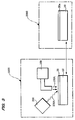
- the migration energy of atoms in a first ceramic film 20c is increased by feeding the active species 100A from the active species feeder 100 and the electromagnetic wave 200A from the electromagnetic wave generating section 200 to the first ceramic film 20c on the substrate 10, as shown in Figure 2, whereby the second ceramic film having high crystallinity can be formed.
- the first ceramic film may be formed of ceramics in an amorphous state or ceramics having low crystallinity.
- the migration energy of atoms is increased by applying the active species 100A and the electromagnetic wave 200A, whereby the second ceramic film having high crystallinity is obtained.
- the thickness of the ceramic film may be 5 nm to 30 nm. If the thickness of the film is within this range, the effect of increasing the migration energy of atoms by the electromagnetic wave and active species can be obtained in the entire film. If the thickness of the film is less than 5 nm, the composition of the film tend to become uneven. If the thickness of the film is more than 30 nm, it is difficult to obtain the effect of increasing the migration energy of atoms in the entire film.
- a ceramic film having a predetermined thickness can be formed by repeating several times a step of forming a thin ceramic film having a predetermined thickness by the first fabrication method. There are following features of this fabrication method.
- the first film 20a is formed on the substrate 10 in a film forming section 2000, as shown in Figure 3.
- the substrate 10 on which the first ceramic film 20a is formed is transferred to a crystallization section 1000.
- the active species 100A and the electromagnetic wave 200A are fed to the first ceramic film 20a respectively from the active species feeder 100 and the electromagnetic wave generating section 200, whereby the first ceramic film 20a is crystallized to form the second ceramic film 20.
- the thickness of the ceramic film or the second ceramic film may be 5-30 nm in the same manner as in the first fabrication method.
- a third fabrication method wherein a ceramic film is not formed on the entire surface of the substrate, but formed in part, specifically, in a minute region. This method has some features as follows.
- a ceramics fabrication device which has following features.
- Figure 1 is a view schematically showing an example of the fabrication method according to the present invention.
- Figure 2 is a view schematically showing an example of the fabrication method according to the present invention.
- Figure 3 is a view schematically showing an example of the fabrication method according to the present invention.
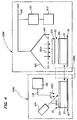
- Figure 4 is a view schematically showing a first embodiment of the fabrication method and fabrication device according to the present invention.
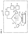
- Figure 5 is a view schematically showing a second embodiment of the fabrication method and fabrication device according to the present invention.
- Figure 6 is a view schematically showing a third embodiment of the fabrication method and fabrication device according to the present invention.
- Figure 7 is a view schematically showing a fourth embodiment of the fabrication method and fabrication device according to the present invention.
- Figure 8 is a view schematically showing a semiconductor device according to a fifth embodiment of the present invention.
- Figure 4 is a view schematically showing a method and a device for fabricating ceramics according to the present embodiment.
- the fabrication device shown in Figure 4 includes a film forming section 2000, a crystallization section 1000, and a load-lock section 3000.
- An object 30 to be treated is disposed so as to be able to go back and forth between the film forming section 2000 and the crystallization section 1000 through the load-lock section 3000.
- the film forming section 2000 includes a raw material tank 410 in which ceramics materials such as organic metals are stored, a mist-forming section 420 which forms a mist of the raw materials, a gas feeding section 430 for feeding carrier gas, and a raw material feeding section 450 for feeding the misted raw materials and gas to a specific region of the substrate 10 placed on a base section 40.
- a mesh 460 is provided at the end of the raw material feeding section 450.
- a mask 470 for patterning the first ceramic film 20a to be formed into a specific pattern is disposed between the substrate 10 and the raw material feeding section 450, as required.
- the base section 40 has a heating section for heating the substrate 10 to a specific temperature.
- the first ceramic film 20a is formed by the following steps.
- the raw materials fed to the mist-forming section 420 from the raw material tank 410 are misted using ultrasonic waves, for example, to form a mist (droplets) with a particle diameter of 0.1 to 0.2 ⁇ m.
- the mist formed in the mist-forming section 420 and gas fed from the gas feeding section 430 are transferred to the raw material feeding section 450.
- Raw material species 300A are fed to the substrate 10 from the raw material feeding section 450, whereby the first ceramic film 20a in an amorphous state is formed on the substrate 10.
- the first ceramic film 20a in an amorphous state is obtained by causing an organic metal complex to decompose (cleaning) by heating the substrate 10. This cleaning may be performed using RTA or a furnace in another room.
- the first ceramic film 20a formed using an LSMCD method has appropriately distributed minute vacancies formed therein, the first ceramic film 20a is advantageous for crystallization because the atoms easily migrate. It is preferable that the first ceramic film 20a be formed to have a thickness of 5-30 nm, for example, in order to ensure effective crystallization in the succeeding crystallization step. If the thickness of the first ceramic film 20a is within this range, the crystal grain size can be decreased by the crystallization treatment without causing unevenness in the composition as described above. Therefore, ceramics having high crystallinity can be obtained.
- the crystallization section 1000 includes an active species feeder 100 and an electromagnetic wave generating section 200.
- Active species 100A formed in the active species feeder 100 are fed to a specific region of the substrate 10 through a feeding passage 110.
- An electromagnetic wave 200A generated in the electromagnetic wave generating section 200 is applied to the region to which the active species 100A are fed.
- the active species feeder 100 and the electromagnetic wave generating section 200 are appropriately disposed so as not to prevent the active species 100A and the electromagnetic wave 200A from being fed.
- the migration energy of atoms in the first ceramic film 20a is increased by applying the active species 100A and the electromagnetic wave 200A to the first ceramic film 20a in an amorphous state formed in the film forming section 2000.
- the first ceramic film 20a is crystallized at a comparatively low temperature, specifically, at a temperature of less than 600°C, and preferably 450°C or less, whereby a second ceramic film 20b having high crystallinity is formed.
- Formation of the first ceramic film 20a in the film forming section 2000 and formation of the crystal ceramic film 20c in the crystallization section 1000 may be repeated several times in order to obtain ceramic films with a specified thickness.
- the growth rate differs depending on the crystal orientation.
- grooves or holes unfavorable for polycrystals tend to be formed.
- a homogenous film can be obtained while filling the above grooves or holes by repeatedly layering thin films as in the present embodiment.
- the first ceramic film 20a in which atoms easily migrate due to the presence of appropriate minute vacancies can be obtained by using an LSMCD method in the film forming section 2000.
- a large amount of migration energy can be provided to atoms by applying the active species 100A and the electromagnetic wave 200A to the first ceramic film 20a in the crystallization section 1000.
- crystallization can be suitably performed at a lower temperature in comparison with conventional devices.
- FIG. 5 is a view schematically showing a film forming section 4000 according to the present embodiment.
- the film forming section 4000 is an example of a device capable of performing formation and crystallization of a film at the same time.
- film formation is performed by MOCVD, with which the crystallization method of the present invention is combined.
- the film forming section 4000 includes a raw material tank 510, a mist-forming section 520, a heater 540, and a raw material feeding section 550 as a system for feeding raw materials.
- the raw material tank 510 and the mist-forming section 520 are the same as the raw material tank 410 and the mist-forming section 420 described in the first embodiment. Therefore, further description is omitted.
- the heater 540 gasifies the misted raw materials by heating. Reactive species 300A are fed to a specific region of the substrate 10 from the raw material feeding section 550.
- the active species feeder 100 and the electromagnetic wave generating section 200 are disposed above the base section 40 at a position so as not to prevent the reactive species 300A from being fed.
- the active species 100A are applied to a specific region of the substrate 10 from the active species feeder 100.
- the electromagnetic wave 200A is applied from the electromagnetic wave generating section 200.
- the wavelength of the electromagnetic wave is preferably 193-300 nm. Use of an electromagnetic wave within this wavelength range increases the migration of atoms in the oxide. Use of ArF at a wavelength of 193 nm as the electromagnetic wave allows oxygen to dissociate, thereby increasing the active species concentration.
- the film forming section 4000 of the present embodiment formation of a ceramic film by MOCVD and crystallization of the film by the active species 100A and the electromagnetic wave 200A are performed at the same time, whereby the ceramic film 20 is formed.
- a large amount of migration energy can be provided to atoms by applying the active species 100A and electromagnetic wave 200A to the ceramic film in the film forming section 4000 at the same time as the film formation.
- crystallization can be suitably performed at a lower temperature in comparison with conventional devices.
- Figure 6 is a view showing an example of a method of feeding the active species 100A and the electromagnetic wave 200A.
- at least one of the active species 100A and the electromagnetic wave 200A, preferably both or at least the electromagnetic wave 200A is partly fed to the object 30 in the region in which the ceramics is formed.
- the active species 100A and the electromagnetic wave 200A are fed to a linear region 30a or a spot-shaped region 30b, as shown in Figure 6.
- the regions 30a and 30b to which the active species 100A and the electromagnetic wave 200A are fed are set so as to be moved relative to the object 30.
- any of a method of moving the object 30, a method of moving the region 30a or 30b, and a method of moving the both of the object 30 and the region 30a or 30b may be employed.
- the region 30a or 30b is moved relative to the object 30 by moving at least one of the object 30 and the region 30a or 30b in a direction intersecting the linear region at right angles (X direction in Figure 6, for example).
- the active species 100A and the electromagnetic wave 200A are fed in the shape of a spot, at least one of the object 30 and the region 30a or 30b is moved in one direction (X direction or Y direction in Figure 6, for example).
- the energy of the active species 100A and the intensity of the electromagnetic wave 200A can be increased while preventing the temperature of the object 30 from increasing in comparison with the case of feeding the active species 100A and the electromagnetic wave 200A onto the entire surface of the object 30.
- the object 30 Since an increase in the intensity of the electromagnetic wave 200A results in an increase in the temperature of the object 30, the object 30 may be damaged due to heat depending on the type of the object 30. For example, in the case where a semiconductor device is formed on the substrate of the object 30, an oxide film may be formed or a MOS device may be damaged due to diffusion of impurities, thereby resulting in deterioration of the semiconductor device.
- an increase in the temperature of the object 30 due to application of the electromagnetic wave can be prevented by specifying the region 30a or 30b.
- the intensity of the electromagnetic wave 200A and the energy of the active species 100A are set while taking into consideration the above-described increase in the temperature of the object, composition of the ceramics, and the like.
- Figures 7A and 7B illustrate a modification example of the film-forming method of the present invention.
- Figure 7A is a plan view showing the substrate 10.
- Figure 7B is a cross-sectional view along the line A-A shown in Figure 7A.
- the present embodiment illustrates an example of forming ceramics on part of the substrate 10. Since the area required to be heated is relatively decreased by partly forming ceramics in comparison with the case of forming ceramics over the entire surface, the amount of energy required for the heating treatment can be decreased. As a result, the temperature of the heating process can be relatively reduced. Therefore, according to the present embodiment, a reduction in the process temperature can be further achieved in addition to the reduction due to application of the active species and electromagnetic wave.
- the substrate 10 includes a first substrate 12, and film-forming sections 14 and a non-film-forming section 16 which are formed on the first substrate 12.
- the film-forming sections 14 are formed using a material having high chemical or physical affinity to the ceramics formed on the substrate 10, such as a material having good wettability with the raw materials or reactive species of the ceramics.
- the non-film-forming section 16 is formed using a material having poor chemical or physical affinity to the ceramics to be formed, such as a material having low wettability with the raw materials or reactive species of the ceramics.
- the ceramic film 20 with a specific pattern is formed by thus arranging the surface of the substrate 10 to dispose the film-forming sections 14 in a region in which it is desired to form a ceramic film 20.
- iridium oxide may be used as the material for the film-forming sections 14, and a fluorine compound may be used as the material for the non-film-forming section 16.
- the method of fabricating ceramics according to the present embodiment can be applied to various types of ceramics such as ferroelectrics.
- the method can be suitably applied to layered perovskite, in particular.
- oxygen in particular, radicals (atomic oxygen) tend to be diffused in a direction intersecting the c-axis at right angles. Therefore, radicals easily migrate from the side of the ceramic film 20 in the heating process for crystallization. As a result, oxygen loss in perovskite is decreased and the polarization characteristics are improved, thereby preventing deterioration of fatigue characteristics, imprint characteristics, and the like.
- Figure 8 illustrates an example of a semiconductor device (ferroelectric memory device 5000) using the ferroelectrics obtained by the fabrication method according to the present invention.
- the ferroelectric memory device 5000 includes a CMOS region R1, and a capacitor region R2 formed on the CMOS region R1.
- the CMOS region R1 has a conventional structure. Specifically, the CMOS region R1 includes a semiconductor substrate 1, an element isolation region 2 and a MOS transistor 3 formed on the semiconductor substrate 1, and an interlayer dielectric 4.
- the capacitor region R2 includes a capacitor C100 consisting of a lower electrode 5, a ferroelectric film 6, and an upper electrode 7, an interconnect layer 8a connected to the lower electrode 5, an interconnect layer 8b connected to the upper electrode 7, and an insulating layer 9.
- An impurity diffusion layer 3a of the MOS transistor 3 and the lower electrode 5 which makes up the capacitor C100 are connected through a contact layer 11 formed of polysilicon or a tungsten plug.
- the ferroelectric (PZT, SBT) film 6 which makes up the capacitor C100 can be formed at a temperature lower than that for conventional ferroelectrics.
- the ferroelectric film 6 can be formed at 500°C or less.
- the ferroelectric film 6 can be formed at less than 600°C. Therefore, since the CMOS region R1 can be prevented from being heat damaged, the capacitor C100 can be applied to highly integrated ferroelectric memory devices.
- ferroelectric (PZT, SBT) film 6 can be formed at a temperature lower than that of conventional ferroelectrics, deterioration of interconnections or electrode sections can be prevented even if expensive materials such as iridium and platinum are not used as the materials for an interconnect layer (not shown) in the CMOS region R1 and the electrode sections 5 and 7 which make up the capacitor C100. Therefore, cheap aluminum alloys can be used as the materials for the interconnect layer and the electrode sections, thereby reducing cost.
- CMOS complementary metal-oxide-semiconductor
- CMOS complementary metal-oxide-semiconductor
- PZT ferroelectrics
- SBT ferroelectrics
- the fabrication method of the present invention since the process temperature for the ferroelectrics can be decreased, capacitors can be continuously formed after performing a multilayer interconnection step, which is the final step in a conventional semiconductor process. Therefore, the number of processes which must be isolated can be decreased, whereby the process can be simplified.
- the fabrication method of the present invention does not need the isolation of the semiconductor process and the capacitor process, the method is advantageous for fabricating a semiconductor device including logic circuits, analog circuits, and the like in combination.
- Dielectrics formed using the fabrication method of the present invention are not limited to the above ferroelectric memory device, but applied to various types of semiconductor devices.
- the capacity of a capacitor can be increased by using paraelectrics with a high dielectric constant such as BST.
- Dielectrics formed using the fabrication method of the present invention may be applied to other applications such as piezoelectrics of piezoelectric devices used for actuators.
- Nitrides (silicon nitride, titanium nitride) formed using the fabrication method of the present invention may be applied to passivation films and local interconnect films of semiconductor devices, and the like.
Landscapes
- Chemical & Material Sciences (AREA)
- Engineering & Computer Science (AREA)
- Organic Chemistry (AREA)
- Chemical Kinetics & Catalysis (AREA)
- General Chemical & Material Sciences (AREA)
- Materials Engineering (AREA)
- Mechanical Engineering (AREA)
- Metallurgy (AREA)
- Health & Medical Sciences (AREA)
- Physics & Mathematics (AREA)
- Optics & Photonics (AREA)
- Inorganic Chemistry (AREA)
- Toxicology (AREA)
- Manufacturing & Machinery (AREA)
- Semiconductor Memories (AREA)
- Chemical Vapour Deposition (AREA)
- Formation Of Insulating Films (AREA)
- Physical Vapour Deposition (AREA)
- Physical Or Chemical Processes And Apparatus (AREA)
Abstract
Description
- (F) Ceramics obtained by the fabrication methods according to the present invention can be used in various types of applications as follows.
- (1) There is provided a semiconductor device comprising a capacitor which includes a dielectric film formed by the fabrication methods of the present invention. As examples of such a semiconductor device, a DRAM which uses paraelectrics obtained by the fabrication methods of the present invention as the dielectric film, a ferroelectric memory (FeRAM) device, and the like can be given.
- (2) There is provided a piezoelectric device comprising a dielectric film formed by the fabrication methods of the present invention.
Claims (51)
- A method of fabricating ceramics, comprising
a step of forming a ceramic film by feeding an electromagnetic wave and an active species of a substance which is at least part of raw materials for the ceramics to a predetermined region. - The method of fabricating ceramics as defined in claim 1, wherein a film including a substance which is part of raw materials for the ceramics is formed in the predetermined region.
- A method of fabricating ceramics, comprising
a step of feeding an active species and an electromagnetic wave to a first ceramic film to form a second ceramic film which has a crystal structure differing from the crystal structure of the first ceramic film. - The method of fabricating ceramics as defined in claim 3, wherein the first ceramic film is formed of ceramics in an amorphous state.
- The method of fabricating ceramics as defined in claim 3, wherein the first ceramic film is formed of ceramics having low crystallinity.
- The method of fabricating ceramics as defined in claim 1 or 2,
wherein the active species of a substance which is at least part of the raw materials for the ceramics is a radical, an ion, or ozone obtained by activating a substance containing oxygen or nitrogen. - The method of fabricating ceramics as defined in any one of claims 3 to 5, wherein the active species is a radical or an ion obtained by activating a substance containing oxygen or nitrogen.
- The method of fabricating ceramics as defined in any one of claims 1 to 7, wherein in addition to the active species, an ion obtained by activating inert gas are also fed to the predetermined region.
- The method of fabricating ceramics as defined in claim 1 or 2, wherein the thickness of the ceramic film is 5 nm to 30 nm.
- The method of fabricating ceramics as defined in any one of claims 3 to 5, wherein the thickness of the second ceramic film is 5 nm to 30 nm.
- A method of fabricating ceramics,
wherein a film having a predetermined thickness is formed by repeating several times a step of forming a ceramic film having a predetermined thickness by feeding at least one of an electromagnetic wave and active species of a substance which is at least part of raw materials for the ceramics to a predetermined region. - The method of fabricating ceramics as defined in claim 11, wherein a film including a substance which is part of the raw materials for the ceramics is formed in the predetermined region.
- The method of fabricating ceramics as defined in claim 11 or 12, wherein the thickness of the ceramic film is 5 nm to 30 nm.
- The method of fabricating ceramics as defined in any one of claims 11 to 13, wherein the ceramic film is formed on part of a substrate.
- A method of fabricating ceramics, comprising:wherein a film having a predetermined thickness is formed by performing alternately the first and second steps.a first step of forming a first ceramic film; anda second step of feeding at least one of an electromagnetic wave and active species to the first ceramic film to form a second ceramic film which has a crystal structure differing from the crystal structure of the first ceramic film,
- The method of fabricating ceramics as defined in claim 15, wherein the thickness of the first ceramic film is 5 nm to 30 nm.
- The method of fabricating ceramics as defined in claim 15 or 16, wherein the first ceramic film is formed on part of a substrate.
- The method of fabricating ceramics as defined in claim 15, wherein the first ceramic film is formed of ceramics in an amorphous state.
- The method of fabricating ceramics as defined in claim 15, wherein the first ceramic film is formed of ceramics having low crystallinity.
- The method of fabricating ceramics as defined in any one of claims 11 to 14,
wherein the active species of a substance which is at least part of the raw materials for the ceramics is a radical, an ion, or ozone obtained by activating a substance containing oxygen or nitrogen. - The method of fabricating ceramics as defined in any one of claims 15 to 19,
wherein the active species is a radical, an ion, or ozone obtained by activating a substance containing oxygen or nitrogen. - The method of fabricating ceramics as defined in any one of claims 11 to 21, wherein in addition to the active species, ions obtained by activating inert gas is also fed to the predetermined region.
- A method of fabricating ceramics,
wherein a region for forming a ceramic film is part of a substrate; and
the method comprising a step of forming the ceramic film by feeding at least one of an electromagnetic wave and active species of a substance which is at least part of raw materials for the ceramics to a predetermined region. - The method of fabricating ceramics as defined in claim 23, wherein a film including a substance which is part of the raw materials for the ceramics is formed in the predetermined region.
- A method of fabricating ceramics,
wherein a region for forming a ceramic film is part of a substrate; and
the method comprising a step of feeding at least one of active species and an electromagnetic wave to a first ceramic film to form a second ceramic film which has a crystal structure differing from the crystal structure of the first ceramic film. - The method of fabricating ceramics as defined in any one of claims 23 to 25, further comprising a step of:forming a film-forming region having affinity to ceramics to be formed and a non-film-forming region having no affinity to ceramics to be formed on a surface of the substrate, to form self-alignably a ceramic film in the film-forming region.
- The method of fabricating ceramics as defined in claim 25 or 26, wherein the first ceramic film is formed of ceramics in an amorphous state.
- The method of fabricating ceramics as defined in claim 25 or 26, wherein the first ceramic film is formed of ceramics having low crystallinity.
- The method of fabricating ceramics as defined in claim 23 or 24,
wherein the active species of a substance which is at least part of the raw materials for the ceramics is a radical, an ion, or ozone obtained by activating a substance containing oxygen or nitrogen. - The method of fabricating ceramics as defined in any one of claims 25 to 28, wherein the active species is a radical or an ion obtained by activating a substance containing oxygen or nitrogen.
- The method of fabricating ceramics as defined in any one of claims 23 to 30, wherein in addition to the active species, ions obtained by activating inert gas are fed to the predetermined region.
- The method of fabricating ceramics as defined in claim 23 or 24, wherein the thickness of the ceramic film is 5 nm to 30 nm.
- The method of fabricating ceramics as defined in any one of claims 25 to 28, wherein the thickness of the second ceramic film is 5 nm to 30 nm.
- The method of fabricating ceramics as defined in any one of claims 23 to 33, wherein the step of forming the ceramics is repeated several times.
- The method of fabricating ceramics as defined in any one of claims 1 to 34,
wherein at least one of the active species and the electromagnetic wave is fed to part of a substrate. - The method of fabricating ceramics as defined in claim 35,
wherein the substrate is relatively moved when at least one of the active species and the electromagnetic wave is fed to the part of the substrate. - The method of fabricating ceramics as defined in claim 3 to 5, 15 to 19, or 25,
wherein the first ceramic film is formed by a coating method, the liquid source misted chemical deposition (LSMCD), the chemical vapor deposition (CVD), or a sputtering method. - The method of fabricating ceramics as defined in claim 37, wherein the first ceramic film is formed by LSMCD or CVD.
- The method of fabricating ceramics as defined in any one of claims 1 to 38,
wherein the ceramic film or the second ceramic film is formed of ferroelectrics. - The method of fabricating ceramics as defined in any one of claims 1 to 39,
wherein the ceramic film or the second ceramic film is formed at a temperature of less than 600°C. - A ceramics fabrication device, comprising:wherein at least one of the active species and the electromagnetic wave is fed to a region for forming the ceramics.a base of a substrate on which ceramics is formed;a heating section;an active species feeder which feeds active species of a substance which is at least part of raw materials for the ceramics; andan electromagnetic wave generating section which provides an electromagnetic wave,
- The ceramics fabrication device as defined in claim 41, further comprising
a film forming section which forms a ceramic film or a film including a substance which is part of the raw materials for the ceramics, in a chamber. - A ceramics fabrication device, comprising:a crystallization section which has a base of a substrate on which ceramics is formed, a heating section, an active species feeder which feeds active species of a substance which is at least part of raw materials for the ceramics, and an electromagnetic wave generating section which provides an electromagnetic wave, to feed at least one of the active species and the electromagnetic wave to a region for forming the ceramics; anda film forming section which is formed in a chamber differing from the chamber of the crystallization section.
- The ceramics fabrication device as defined in claim 43, further comprising a load-lock section between the crystallization section and the film forming section.
- The ceramics fabrication device as defined in any one of claims 41 to 44, wherein the base of the substrate functions as the heating section.
- The ceramics fabrication device as defined in any one of claims 41 to 45,
wherein at least one of the active species feeder and the electromagnetic wave generating section feeds at least one of the active species and the electromagnetic wave to part of the substrate. - The ceramics fabrication device as defined in claim 46,
wherein the substrate is relatively moved when at least one of the active species and the electromagnetic wave is fed to the part of the substrate. - The device for fabricating ceramics as defined in claim 43,
wherein the film forming section forms a film by a coating method, the liquid source misted chemical deposition (LSMCD), the chemical vapor deposition (CVD), or a sputtering method. - The device for fabricating ceramics as defined in claim 48, wherein the film forming section forms a film by LSMCD or CVD.
- A semiconductor device comprising a capacitor which includes a dielectric film formed by the fabrication method as defined in any one of claims 1 to 40.
- A piezoelectric device comprising a dielectric film formed by the fabrication method as defined in any one of claims 1 to 40.
Applications Claiming Priority (3)
| Application Number | Priority Date | Filing Date | Title |
|---|---|---|---|
| JP2000091603A JP3664033B2 (en) | 2000-03-29 | 2000-03-29 | Ceramic manufacturing method and manufacturing apparatus thereof |
| JP2000091603 | 2000-03-29 | ||
| PCT/JP2001/002631 WO2001073161A1 (en) | 2000-03-29 | 2001-03-29 | Method for producing ceramic and apparatus for producing the same, semiconductor device, and piezoelectric device |
Publications (2)
| Publication Number | Publication Date |
|---|---|
| EP1205575A1 true EP1205575A1 (en) | 2002-05-15 |
| EP1205575A4 EP1205575A4 (en) | 2003-04-16 |
Family
ID=18607050
Family Applications (1)
| Application Number | Title | Priority Date | Filing Date |
|---|---|---|---|
| EP01917596A Withdrawn EP1205575A4 (en) | 2000-03-29 | 2001-03-29 | PROCESS FOR PRODUCING CERAMIC AND APPARATUS FOR PRODUCING SAME, SEMICONDUCTOR DEVICE AND PIEZOELECTRIC DEVICE |
Country Status (6)
| Country | Link |
|---|---|
| US (1) | US20020031846A1 (en) |
| EP (1) | EP1205575A4 (en) |
| JP (1) | JP3664033B2 (en) |
| KR (1) | KR100449774B1 (en) |
| CN (1) | CN1302151C (en) |
| WO (1) | WO2001073161A1 (en) |
Families Citing this family (8)
| Publication number | Priority date | Publication date | Assignee | Title |
|---|---|---|---|---|
| US6730367B2 (en) * | 2002-03-05 | 2004-05-04 | Micron Technology, Inc. | Atomic layer deposition method with point of use generated reactive gas species |
| JP2003298020A (en) * | 2002-03-29 | 2003-10-17 | Seiko Epson Corp | Method of forming ferroelectric thin film, ferroelectric memory, method of manufacturing ferroelectric memory, semiconductor device, and method of manufacturing semiconductor device |
| JP2003298021A (en) * | 2002-03-29 | 2003-10-17 | Seiko Epson Corp | Method of forming ferroelectric thin film, ferroelectric memory, method of manufacturing ferroelectric memory, semiconductor device, and method of manufacturing semiconductor device |
| US20060255486A1 (en) * | 2005-05-10 | 2006-11-16 | Benson Olester Jr | Method of manufacturing composite optical body containing inorganic fibers |
| JP2011124441A (en) * | 2009-12-11 | 2011-06-23 | Utec:Kk | Method for manufacturing crystallized film and crystallization apparatus |
| JP5951542B2 (en) * | 2013-03-28 | 2016-07-13 | 住友重機械工業株式会社 | Deposition equipment |
| JP6704133B2 (en) * | 2015-12-24 | 2020-06-03 | 株式会社Flosfia | Manufacturing method of perovskite film |
| CN114229962B (en) * | 2021-10-08 | 2022-12-06 | 同济大学 | Electrochemical tubular ceramic membrane for water treatment and preparation method and application thereof |
Family Cites Families (10)
| Publication number | Priority date | Publication date | Assignee | Title |
|---|---|---|---|---|
| JPS6175529A (en) * | 1984-09-21 | 1986-04-17 | Toshiba Corp | Dry etching method and apparatus therefor |
| JP2635021B2 (en) * | 1985-09-26 | 1997-07-30 | 宣夫 御子柴 | Deposition film forming method and apparatus used for the same |
| JPH0680656B2 (en) * | 1987-11-13 | 1994-10-12 | シャープ株式会社 | Method for forming oxide thin film |
| JPH02200782A (en) * | 1989-01-31 | 1990-08-09 | Matsushita Electric Ind Co Ltd | Formation of lead titanate thin film |
| US5192393A (en) * | 1989-05-24 | 1993-03-09 | Hitachi, Ltd. | Method for growing thin film by beam deposition and apparatus for practicing the same |
| JPH0353068A (en) * | 1989-07-20 | 1991-03-07 | Matsushita Electric Ind Co Ltd | Method for plotting film by laser cvd |
| JP3407204B2 (en) * | 1992-07-23 | 2003-05-19 | オリンパス光学工業株式会社 | Ferroelectric integrated circuit and method of manufacturing the same |
| US5527731A (en) * | 1992-11-13 | 1996-06-18 | Hitachi, Ltd. | Surface treating method and apparatus therefor |
| JP3450463B2 (en) * | 1994-10-24 | 2003-09-22 | 株式会社日立製作所 | Method for manufacturing semiconductor device |
| US6120846A (en) * | 1997-12-23 | 2000-09-19 | Advanced Technology Materials, Inc. | Method for the selective deposition of bismuth based ferroelectric thin films by chemical vapor deposition |
-
2000
- 2000-03-29 JP JP2000091603A patent/JP3664033B2/en not_active Expired - Fee Related
-
2001
- 2001-03-29 EP EP01917596A patent/EP1205575A4/en not_active Withdrawn
- 2001-03-29 US US09/819,687 patent/US20020031846A1/en not_active Abandoned
- 2001-03-29 KR KR10-2001-7015256A patent/KR100449774B1/en not_active Expired - Fee Related
- 2001-03-29 CN CNB018007066A patent/CN1302151C/en not_active Expired - Fee Related
- 2001-03-29 WO PCT/JP2001/002631 patent/WO2001073161A1/en not_active Ceased
Also Published As
| Publication number | Publication date |
|---|---|
| KR20020020897A (en) | 2002-03-16 |
| JP3664033B2 (en) | 2005-06-22 |
| CN1302151C (en) | 2007-02-28 |
| EP1205575A4 (en) | 2003-04-16 |
| CN1365400A (en) | 2002-08-21 |
| US20020031846A1 (en) | 2002-03-14 |
| JP2001279443A (en) | 2001-10-10 |
| KR100449774B1 (en) | 2004-09-22 |
| WO2001073161A1 (en) | 2001-10-04 |
Similar Documents
| Publication | Publication Date | Title |
|---|---|---|
| EP0708983B1 (en) | Chemical vapor deposition process for fabricating layered superlattice materials | |
| KR100363081B1 (en) | Thin film formation apparatus | |
| EP0747937A2 (en) | Ferroelectric thin film coated substrate, producing method thereof and capacitor structure element using thereof | |
| KR100763559B1 (en) | Formation method of ferroelectric film and manufacturing method of ferroelectric capacitor using same | |
| US7001778B2 (en) | Method of making layered superlattice material with improved microstructure | |
| EP0747938A2 (en) | Ferroelectric thin film coated substrate, producing method thereof and capacitor structure element using thereof | |
| GB2364825A (en) | A capacitor using a tantalum nitride dielectric | |
| EP1205575A1 (en) | Method for producing ceramic and apparatus for producing the same, semiconductor device, and piezoelectric device | |
| US7811834B2 (en) | Methods of forming a ferroelectric layer and methods of manufacturing a ferroelectric capacitor including the same | |
| JP2001127258A (en) | Semiconductor device and method of manufacturing the same | |
| US20030175425A1 (en) | Vapor phase deposition method for metal oxide dielectric film | |
| US6610211B1 (en) | Method of processing internal surfaces of a chemical vapor deposition reactor | |
| KR20010085328A (en) | Vapor growth method for metal oxide dielectric film and vapor growth device for metal oxide dielectric material | |
| EP1205576B1 (en) | Method for producing ceramic | |
| US20040113186A1 (en) | Method of making layered superlattice material with ultra-thin top layer | |
| KR100315885B1 (en) | Dielectric thin film formation method for use in electronic components | |
| JPH0689986A (en) | Electronic device and its manufacturing method | |
| JP4557144B2 (en) | Manufacturing method of ceramics | |
| KR100382742B1 (en) | Method for forming capacitor of semiconductor device | |
| JP4330907B2 (en) | Method for manufacturing metal oxide film and method for manufacturing capacitor element | |
| WO2002073680A2 (en) | Method of making layered superlattice material with ultra-thin top layer | |
| JP2007081410A (en) | Ferroelectric film, ferroelectric capacitor forming method, and ferroelectric capacitor | |
| CN100388420C (en) | Method for fabricating layered superlattice materials with improved microstructure | |
| HK1076540B (en) | Method of making layered superlattice material with improved microstructure |
Legal Events
| Date | Code | Title | Description |
|---|---|---|---|
| PUAI | Public reference made under article 153(3) epc to a published international application that has entered the european phase |
Free format text: ORIGINAL CODE: 0009012 |
|
| 17P | Request for examination filed |
Effective date: 20011218 |
|
| AK | Designated contracting states |
Kind code of ref document: A1 Designated state(s): AT BE CH CY DE DK ES FI FR GB GR IE IT LI LU MC NL PT SE TR |
|
| A4 | Supplementary search report drawn up and despatched |
Effective date: 20030228 |
|
| RIC1 | Information provided on ipc code assigned before grant |
Ipc: 7H 01L 27/10 B Ipc: 7C 23C 16/452 B Ipc: 7C 23C 16/48 B Ipc: 7H 01L 41/22 B Ipc: 7C 23C 16/40 A Ipc: 7H 01L 21/31 B Ipc: 7H 01L 21/316 B Ipc: 7H 01L 41/24 B Ipc: 7C 23C 14/08 B Ipc: 7C 23C 14/22 B |
|
| 17Q | First examination report despatched |
Effective date: 20030826 |
|
| RBV | Designated contracting states (corrected) |
Designated state(s): DE FR GB IT |
|
| STAA | Information on the status of an ep patent application or granted ep patent |
Free format text: STATUS: THE APPLICATION IS DEEMED TO BE WITHDRAWN |
|
| 18D | Application deemed to be withdrawn |
Effective date: 20051209 |