EP1204304A2 - Etched tri-layer metal bonding layer - Google Patents
Etched tri-layer metal bonding layer Download PDFInfo
- Publication number
- EP1204304A2 EP1204304A2 EP01125895A EP01125895A EP1204304A2 EP 1204304 A2 EP1204304 A2 EP 1204304A2 EP 01125895 A EP01125895 A EP 01125895A EP 01125895 A EP01125895 A EP 01125895A EP 1204304 A2 EP1204304 A2 EP 1204304A2
- Authority
- EP
- European Patent Office
- Prior art keywords
- metallic
- layer
- strip
- broadsides
- bonding
- Prior art date
- Legal status (The legal status is an assumption and is not a legal conclusion. Google has not performed a legal analysis and makes no representation as to the accuracy of the status listed.)
- Granted
Links
- 229910052751 metal Inorganic materials 0.000 title description 8
- 239000002184 metal Substances 0.000 title description 8
- 238000000034 method Methods 0.000 claims abstract description 22
- 229910052782 aluminium Inorganic materials 0.000 claims abstract description 20
- XAGFODPZIPBFFR-UHFFFAOYSA-N aluminium Chemical compound [Al] XAGFODPZIPBFFR-UHFFFAOYSA-N 0.000 claims abstract description 20
- 239000007769 metal material Substances 0.000 claims abstract description 16
- RYGMFSIKBFXOCR-UHFFFAOYSA-N Copper Chemical compound [Cu] RYGMFSIKBFXOCR-UHFFFAOYSA-N 0.000 claims abstract description 14
- 229910052802 copper Inorganic materials 0.000 claims abstract description 14
- 239000010949 copper Substances 0.000 claims abstract description 14
- IHQKEDIOMGYHEB-UHFFFAOYSA-M sodium dimethylarsinate Chemical class [Na+].C[As](C)([O-])=O IHQKEDIOMGYHEB-UHFFFAOYSA-M 0.000 claims description 23
- PXHVJJICTQNCMI-UHFFFAOYSA-N Nickel Chemical compound [Ni] PXHVJJICTQNCMI-UHFFFAOYSA-N 0.000 claims description 16
- ATJFFYVFTNAWJD-UHFFFAOYSA-N Tin Chemical compound [Sn] ATJFFYVFTNAWJD-UHFFFAOYSA-N 0.000 claims description 9
- 229910052718 tin Inorganic materials 0.000 claims description 9
- 229910052759 nickel Inorganic materials 0.000 claims description 8
- 238000007654 immersion Methods 0.000 claims description 7
- BASFCYQUMIYNBI-UHFFFAOYSA-N platinum Chemical compound [Pt] BASFCYQUMIYNBI-UHFFFAOYSA-N 0.000 claims description 7
- 239000011135 tin Substances 0.000 claims description 7
- KDLHZDBZIXYQEI-UHFFFAOYSA-N Palladium Chemical compound [Pd] KDLHZDBZIXYQEI-UHFFFAOYSA-N 0.000 claims description 6
- 238000000151 deposition Methods 0.000 claims description 6
- 239000000463 material Substances 0.000 claims description 6
- 230000003213 activating effect Effects 0.000 claims description 5
- 229910045601 alloy Inorganic materials 0.000 claims description 4
- 239000000956 alloy Substances 0.000 claims description 4
- 238000005253 cladding Methods 0.000 claims description 3
- KUNSUQLRTQLHQQ-UHFFFAOYSA-N copper tin Chemical compound [Cu].[Sn] KUNSUQLRTQLHQQ-UHFFFAOYSA-N 0.000 claims description 3
- 239000010931 gold Substances 0.000 claims description 3
- CLDVQCMGOSGNIW-UHFFFAOYSA-N nickel tin Chemical compound [Ni].[Sn] CLDVQCMGOSGNIW-UHFFFAOYSA-N 0.000 claims description 3
- 229910000510 noble metal Inorganic materials 0.000 claims description 3
- 229910052763 palladium Inorganic materials 0.000 claims description 3
- 229910052697 platinum Inorganic materials 0.000 claims description 3
- 229910052703 rhodium Inorganic materials 0.000 claims description 3
- 239000010948 rhodium Substances 0.000 claims description 3
- MHOVAHRLVXNVSD-UHFFFAOYSA-N rhodium atom Chemical compound [Rh] MHOVAHRLVXNVSD-UHFFFAOYSA-N 0.000 claims description 3
- VYZAMTAEIAYCRO-UHFFFAOYSA-N Chromium Chemical compound [Cr] VYZAMTAEIAYCRO-UHFFFAOYSA-N 0.000 claims description 2
- BQCADISMDOOEFD-UHFFFAOYSA-N Silver Chemical compound [Ag] BQCADISMDOOEFD-UHFFFAOYSA-N 0.000 claims description 2
- HSSJULAPNNGXFW-UHFFFAOYSA-N [Co].[Zn] Chemical compound [Co].[Zn] HSSJULAPNNGXFW-UHFFFAOYSA-N 0.000 claims description 2
- 229910052804 chromium Inorganic materials 0.000 claims description 2
- 239000011651 chromium Substances 0.000 claims description 2
- PCHJSUWPFVWCPO-UHFFFAOYSA-N gold Chemical compound [Au] PCHJSUWPFVWCPO-UHFFFAOYSA-N 0.000 claims description 2
- 229910052737 gold Inorganic materials 0.000 claims description 2
- 230000013011 mating Effects 0.000 claims description 2
- QELJHCBNGDEXLD-UHFFFAOYSA-N nickel zinc Chemical compound [Ni].[Zn] QELJHCBNGDEXLD-UHFFFAOYSA-N 0.000 claims description 2
- 229910052709 silver Inorganic materials 0.000 claims description 2
- 239000004332 silver Substances 0.000 claims description 2
- 229910001128 Sn alloy Inorganic materials 0.000 claims 1
- TVZPLCNGKSPOJA-UHFFFAOYSA-N copper zinc Chemical compound [Cu].[Zn] TVZPLCNGKSPOJA-UHFFFAOYSA-N 0.000 claims 1
- 230000008021 deposition Effects 0.000 claims 1
- 230000004888 barrier function Effects 0.000 abstract description 19
- 238000004519 manufacturing process Methods 0.000 abstract description 6
- 238000009792 diffusion process Methods 0.000 abstract description 5
- 235000008429 bread Nutrition 0.000 abstract 2
- 230000002401 inhibitory effect Effects 0.000 abstract 1
- 230000009972 noncorrosive effect Effects 0.000 abstract 1
- 238000005260 corrosion Methods 0.000 description 4
- 230000007797 corrosion Effects 0.000 description 4
- 150000002739 metals Chemical group 0.000 description 4
- 239000000654 additive Substances 0.000 description 3
- 230000000996 additive effect Effects 0.000 description 3
- 229910052725 zinc Inorganic materials 0.000 description 3
- 239000011701 zinc Substances 0.000 description 3
- HCHKCACWOHOZIP-UHFFFAOYSA-N Zinc Chemical compound [Zn] HCHKCACWOHOZIP-UHFFFAOYSA-N 0.000 description 2
- 229910001369 Brass Inorganic materials 0.000 description 1
- 229910000906 Bronze Inorganic materials 0.000 description 1
- 239000010951 brass Substances 0.000 description 1
- 239000010974 bronze Substances 0.000 description 1
- 238000003486 chemical etching Methods 0.000 description 1
- 238000010276 construction Methods 0.000 description 1
- 238000010438 heat treatment Methods 0.000 description 1
- 229910001092 metal group alloy Inorganic materials 0.000 description 1
- 238000007747 plating Methods 0.000 description 1
Images
Classifications
-
- B—PERFORMING OPERATIONS; TRANSPORTING
- B32—LAYERED PRODUCTS
- B32B—LAYERED PRODUCTS, i.e. PRODUCTS BUILT-UP OF STRATA OF FLAT OR NON-FLAT, e.g. CELLULAR OR HONEYCOMB, FORM
- B32B15/00—Layered products comprising a layer of metal
- B32B15/01—Layered products comprising a layer of metal all layers being exclusively metallic
- B32B15/018—Layered products comprising a layer of metal all layers being exclusively metallic one layer being formed of a noble metal or a noble metal alloy
-
- B—PERFORMING OPERATIONS; TRANSPORTING
- B32—LAYERED PRODUCTS
- B32B—LAYERED PRODUCTS, i.e. PRODUCTS BUILT-UP OF STRATA OF FLAT OR NON-FLAT, e.g. CELLULAR OR HONEYCOMB, FORM
- B32B15/00—Layered products comprising a layer of metal
- B32B15/01—Layered products comprising a layer of metal all layers being exclusively metallic
- B32B15/017—Layered products comprising a layer of metal all layers being exclusively metallic one layer being formed of aluminium or an aluminium alloy, another layer being formed of an alloy based on a non ferrous metal other than aluminium
-
- C—CHEMISTRY; METALLURGY
- C23—COATING METALLIC MATERIAL; COATING MATERIAL WITH METALLIC MATERIAL; CHEMICAL SURFACE TREATMENT; DIFFUSION TREATMENT OF METALLIC MATERIAL; COATING BY VACUUM EVAPORATION, BY SPUTTERING, BY ION IMPLANTATION OR BY CHEMICAL VAPOUR DEPOSITION, IN GENERAL; INHIBITING CORROSION OF METALLIC MATERIAL OR INCRUSTATION IN GENERAL
- C23C—COATING METALLIC MATERIAL; COATING MATERIAL WITH METALLIC MATERIAL; SURFACE TREATMENT OF METALLIC MATERIAL BY DIFFUSION INTO THE SURFACE, BY CHEMICAL CONVERSION OR SUBSTITUTION; COATING BY VACUUM EVAPORATION, BY SPUTTERING, BY ION IMPLANTATION OR BY CHEMICAL VAPOUR DEPOSITION, IN GENERAL
- C23C2/00—Hot-dipping or immersion processes for applying the coating material in the molten state without affecting the shape; Apparatus therefor
- C23C2/26—After-treatment
-
- C—CHEMISTRY; METALLURGY
- C23—COATING METALLIC MATERIAL; COATING MATERIAL WITH METALLIC MATERIAL; CHEMICAL SURFACE TREATMENT; DIFFUSION TREATMENT OF METALLIC MATERIAL; COATING BY VACUUM EVAPORATION, BY SPUTTERING, BY ION IMPLANTATION OR BY CHEMICAL VAPOUR DEPOSITION, IN GENERAL; INHIBITING CORROSION OF METALLIC MATERIAL OR INCRUSTATION IN GENERAL
- C23C—COATING METALLIC MATERIAL; COATING MATERIAL WITH METALLIC MATERIAL; SURFACE TREATMENT OF METALLIC MATERIAL BY DIFFUSION INTO THE SURFACE, BY CHEMICAL CONVERSION OR SUBSTITUTION; COATING BY VACUUM EVAPORATION, BY SPUTTERING, BY ION IMPLANTATION OR BY CHEMICAL VAPOUR DEPOSITION, IN GENERAL
- C23C2/00—Hot-dipping or immersion processes for applying the coating material in the molten state without affecting the shape; Apparatus therefor
- C23C2/26—After-treatment
- C23C2/28—Thermal after-treatment, e.g. treatment in oil bath
-
- C—CHEMISTRY; METALLURGY
- C23—COATING METALLIC MATERIAL; COATING MATERIAL WITH METALLIC MATERIAL; CHEMICAL SURFACE TREATMENT; DIFFUSION TREATMENT OF METALLIC MATERIAL; COATING BY VACUUM EVAPORATION, BY SPUTTERING, BY ION IMPLANTATION OR BY CHEMICAL VAPOUR DEPOSITION, IN GENERAL; INHIBITING CORROSION OF METALLIC MATERIAL OR INCRUSTATION IN GENERAL
- C23C—COATING METALLIC MATERIAL; COATING MATERIAL WITH METALLIC MATERIAL; SURFACE TREATMENT OF METALLIC MATERIAL BY DIFFUSION INTO THE SURFACE, BY CHEMICAL CONVERSION OR SUBSTITUTION; COATING BY VACUUM EVAPORATION, BY SPUTTERING, BY ION IMPLANTATION OR BY CHEMICAL VAPOUR DEPOSITION, IN GENERAL
- C23C26/00—Coating not provided for in groups C23C2/00 - C23C24/00
-
- H—ELECTRICITY
- H05—ELECTRIC TECHNIQUES NOT OTHERWISE PROVIDED FOR
- H05K—PRINTED CIRCUITS; CASINGS OR CONSTRUCTIONAL DETAILS OF ELECTRIC APPARATUS; MANUFACTURE OF ASSEMBLAGES OF ELECTRICAL COMPONENTS
- H05K3/00—Apparatus or processes for manufacturing printed circuits
- H05K3/02—Apparatus or processes for manufacturing printed circuits in which the conductive material is applied to the surface of the insulating support and is thereafter removed from such areas of the surface which are not intended for current conducting or shielding
- H05K3/022—Processes for manufacturing precursors of printed circuits, i.e. copper-clad substrates
-
- H—ELECTRICITY
- H05—ELECTRIC TECHNIQUES NOT OTHERWISE PROVIDED FOR
- H05K—PRINTED CIRCUITS; CASINGS OR CONSTRUCTIONAL DETAILS OF ELECTRIC APPARATUS; MANUFACTURE OF ASSEMBLAGES OF ELECTRICAL COMPONENTS
- H05K2201/00—Indexing scheme relating to printed circuits covered by H05K1/00
- H05K2201/03—Conductive materials
- H05K2201/0332—Structure of the conductor
- H05K2201/0335—Layered conductors or foils
- H05K2201/0361—Etched tri-metal structure, i.e. metal layers or metal patterns on both sides of a different central metal layer which is later at least partly etched
Definitions
- This invention relates generally to circuit boards and more particularly to a tri-metallic material construction for use in Etched-Tri-Metal, "ETM", multi-layer circuit boards.
- PCBs printed circuit boards
- U.S. Patent Number 3,801,388 issued April 2, 1974 to Akiyama et al. which is a subtractive process.
- U.S. Patent 4,404,059 issued September 13, 1983 to Livshits et al is an additive process.
- U.S. Patent Number 5,738,797 issued April 14, 1998 to Belke, Jr. et al is assigned to a common assignee. All three of which are incorporated herein by reference.
- These patents describe various additive and subtractive plating and chemical etching processes for constructing multi-layer PCBs having air bridges.
- tri-metallic materials as used in the manufacture of PCBs are a sandwich of aluminum as the middle layer and copper as the top and bottom layers.
- the layers are typically bonded together with a zinc bonding layer. Due to the anodic nature of zinc relative to copper and its position in the Electromotive Force Series, EMF series, the zinc layer is prone to corrosion.
- the tri-metallic material for use in multi-layer printed circuit boards having a first metallic layer with spaced-apart top and bottom broadsides.
- a second and third metallic layers having spaced-apart top and bottom broadsides for overlying the first layer.
- a metallic bonding layer is deposited on the top and bottom broadsides of the first metallic layer that is sandwiched between the second and third metallic layers. The bonding layer bonds the second and third metallic layers to the top and bottom broadsides respectively of the first metallic layer.
- the first metallic layer is aluminum and the second and third metallic layers are copper with the bonding layer being a noble metal.
- the bonding layer in one embodiment is immersion tin deposited on the broadside surfaces of the aluminum. A thin layer of nickel is deposited on the tin, and a copper layer is plated on the nickel layer.
- a barrier layer is desired, to prevent diffusion between layers, the process is the same as is the material of the layer. However some metals function better as a diffusion barrier than they do as a bonding layer.
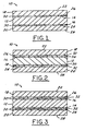
- FIG. 1 a cross-section of the tri-metallic material 10, or sandwich, as used in multi-layer printed circuit boards.
- the tri-metallic material 10 has a first metallic layer 12 with spaced-apart top 14 and bottom 16 broadsides. Second 18 and third 20 metallic layers having spaced-apart top 22, 24 and bottom 26, 28 broadsides for overlying the first layer.
- a metallic seed 30 or barrier 32 layer is deposited on the top 14 and bottom 16 broadsides of the first metallic layer 12 that is sandwiched between the second 18 and third 20 metallic layers.
- the bonding layer 30 bonds the second and third metallic layers to the top 14 and bottom 16 broadsides respectively of the first metallic layer 12.
- the term "barrier layer” is a layer 32 that prevents diffusion from one layer to the other and the term “bonding layer” is a layer 30 that helps in the boding between the layers on either side.
- Both seed and barrier layers 30, 32 are on the order of less than ten microns thick, while the first metal layer 12 in the tri-metallic material 10 is typically approximately one hundred fifty microns thick and the second 18 and third 20 layers are approximately fifty microns thick.
- the phrases bonding layer and barrier layer are used herein interchangeably.
- the first metallic layer 12 is aluminum and the second 18 and third 20 metallic layers are copper with the bonding layer 30 being a noble metal.
- the bonding layer 30 is immersion tin deposited on the broadside surfaces 14, 16 of the aluminum. A thin layer or strike of nickel is deposited on the tin, and the second 18 or third 20 layer, a copper layer is plated on the nickel layer.
- the bonding layer 30 can be tin (Sn), silver (Ag), rhodium, palladium, platinum, (Pt) or gold (Au).
- Sn tin
- Ag silver
- Pt rhodium
- Au gold
- EMF Electromotive Force Series
- Various metal alloys such as bronze (copper-tin) and brass can be used as the bonding layer 30. Each of these alloys is immersion coated onto the aluminum, which would be the first metallic layer. These alloys exhibit good corrosion resistance and have good adhesion with the aluminum layer.
- the preferred metals are chromium, rhodium, palladium and platinum.
- the preferred alloys are zinc-nickel, cobalt-zinc and nickel-tin.
- any of the previous metals be it used for a bonding layer 30 or a barrier layer 32 contains properties that will function both as a bonding layer and a barrier layer.
- the lists in the previous paragraphs indicate those preferred metals to use if only a seed 30 or barrier 32 layer is wanted.
- the bonding layer 30 may be coated on the second 18 and third 20 metallic layers.
- all of the metal layers are sheets of metal that have substantially the same broadside area.
- a method for bonding aluminum and copper in the etched tri-metallic material has the steps of initially securing first 12, second 18 and third 20 metallic strips having spaced-apart top 14, 22, or 24 and bottom 16, 26, or 28 broadsides.
- the first, second and third strip broadsides have substantially identical planar areas.
- a metallic bonding layer 30 or a barrier layer 32 is deposited on both, top 14 and bottom 16 broadside surfaces of the first strip 12.
- the metallic bonding layer 30 is deposited on one broadside surface 26, 24 of each of the second 18 and third 20 strips.
- a barrier layer 32 is deposited on the bottom surface 26 of the second 18 layer 18 and the top surface 24 of the third 20 layer and over the barrier layer 32 is a bonding layer is deposited. As illustrated the bonding layer is directly in contact with the first layer 12, however, either the seed or barrier layer can be in direct contact with the first layer.
- a barrier layer 32 is sandwiched between two bonding layers 30. In turn this sandwich 32-30-32, is located between the first strip 12 and either the second 18 or their strip 20.
- the three strips 12, 18, 20 are then formed into a sandwich wherein the second 18 and third 20 strip overlie respectively the top 14 and bottom 16 broadsides of the first strip 12, such that the bonding layer 30 or barrier layer 32 are not exposed.
- the sandwich is then activated by a heat treatment or cladding for bonding the mating broadside surfaces of the three strips forming a unitary structure.
- the first strip 12 is aluminum and the second 18 and third 20 strips are copper.
- the metallic bonding layer 30 or barrier layer 32 are deposited on the both 14,16 broadsides of the aluminum strip. Depositing is by the process of immersion of both of the broadsides of the aluminum strip or one of the broadside surfaces of the second 18 or third 20 strips which are both copper, with the metallic bonding layer 30.
- the step of activating is by means of heat-treating the sandwich 10 at predetermined temperatures and pressures.
- the step of activating is by means of cladding the sandwich 10 at predetermined pressures and temperatures.
Landscapes
- Chemical & Material Sciences (AREA)
- Engineering & Computer Science (AREA)
- Organic Chemistry (AREA)
- Metallurgy (AREA)
- Chemical Kinetics & Catalysis (AREA)
- Materials Engineering (AREA)
- Mechanical Engineering (AREA)
- Physics & Mathematics (AREA)
- Manufacturing & Machinery (AREA)
- Microelectronics & Electronic Packaging (AREA)
- Oil, Petroleum & Natural Gas (AREA)
- Thermal Sciences (AREA)
- Laminated Bodies (AREA)
- Parts Printed On Printed Circuit Boards (AREA)
- Manufacturing Of Printed Wiring (AREA)
- Insulated Metal Substrates For Printed Circuits (AREA)
Abstract
Description
Claims (12)
- A method for bonding aluminum and copper in an etched tri-metal material, the method comprising:securing a first metallic strip having spaced-apart top and bottom broadsides;securing a second metallic strip, each second strip having spaced-apart top and bottom broadsides;securing a third metallic strip, each third strip having spaced-apart top and bottom broadsides;the first, second and third strip broadsides having substantially identical planar areas;depositing a metallic bonding layer on the broadside surfaces of the first strip or on one broadside surface of each of the second and third strips;forming a sandwich wherein the second strip and the third strip overlie respectively the top and bottom broadsides of the first strip, such that the bonding layers are not exposed; andactivating the bonding layers for bonding the mating broadside surfaces of the first strip and the second and third strip forming a unitary structure.
- The method according to claim 1 wherein the first strip is an aluminum strip and the second and third strips are copper strips.
- The method according to claim 2 wherein said step of depositing the metallic bonding layer is by depositing the metallic bonding layer on the aluminum strip.
- The method according to claim 2 wherein said step of depositing is by the process of immersion both of the broadside surfaces of the aluminum strip or one of the broadside surfaces of the second and third strip with the metallic bonding layer.
- The method according to claim 2 wherein said bonding layer is selected from the group consisting of chromium, nickel, silver, tin, rhodium, palladium, platinum, and gold.
- The method according to claim 2 wherein the bonding layer is selected from a group of alloys consisting of zinc-nickel, copper-tin, copper-zinc, cobalt-zinc, and nickel-tin.
- The method according to claim 6 wherein the nickel-tin alloy is formed by an immersion tin deposition on the first strip followed by a nickel strike.
- The method according to claim 1 wherein said step of activating is by means of heat-treating the sandwich.
- The method according to claim 1 wherein said step of activating is by means of cladding the sandwich.
- A tri-metallic material for use in multi-layer printed circuit boards, said material comprising:a first metallic layer having spaced-apart top and bottom broadsides;a second metallic layer having spaced-apart top and bottom broadsides;a third metallic layer having spaced-apart top and bottom broadsides; anda metallic bonding layer deposited between said top and bottom broadsides of said first metallic layer and said second and third metallic layers respectively;said first metallic layer sandwiched being between said second and third metallic layers, said second and third metallic layers bonded to top and bottom broadsides respectively of said first metallic layer.
- The tri-metallic material according to claim 10 wherein said first metallic layer is aluminum and said second and third metallic layers are copper and said bonding layer is a noble metal.
- The tri-metallic material according to claim 10 wherein:said first metallic layer is aluminum;said metallic bonding layer is immersion tin deposited on said broadside surfaces of said aluminum;a thin layer of nickel is deposited on said tin; andsaid second and third metallic layers are copper plated on said nickel layer.
Applications Claiming Priority (2)
| Application Number | Priority Date | Filing Date | Title |
|---|---|---|---|
| US09/703,815 US6459041B1 (en) | 2000-11-01 | 2000-11-01 | Etched tri-layer metal bonding layer |
| US703815 | 2000-11-01 |
Publications (3)
| Publication Number | Publication Date |
|---|---|
| EP1204304A2 true EP1204304A2 (en) | 2002-05-08 |
| EP1204304A3 EP1204304A3 (en) | 2002-12-11 |
| EP1204304B1 EP1204304B1 (en) | 2004-12-29 |
Family
ID=24826877
Family Applications (1)
| Application Number | Title | Priority Date | Filing Date |
|---|---|---|---|
| EP01125895A Expired - Lifetime EP1204304B1 (en) | 2000-11-01 | 2001-10-30 | Etched tri-layer metal bonding layer |
Country Status (4)
| Country | Link |
|---|---|
| US (1) | US6459041B1 (en) |
| EP (1) | EP1204304B1 (en) |
| JP (1) | JP2002208762A (en) |
| DE (1) | DE60108052T2 (en) |
Families Citing this family (5)
| Publication number | Priority date | Publication date | Assignee | Title |
|---|---|---|---|---|
| JP4746852B2 (en) * | 2004-06-30 | 2011-08-10 | ソニーケミカル&インフォメーションデバイス株式会社 | Transmission cable manufacturing method |
| US7583115B2 (en) * | 2004-08-26 | 2009-09-01 | Micron Technology, Inc. | Delay line off-state control with power reduction |
| JP2007193999A (en) * | 2006-01-17 | 2007-08-02 | Sony Chemical & Information Device Corp | Transmission cable |
| US7696439B2 (en) * | 2006-05-17 | 2010-04-13 | Tessera, Inc. | Layered metal structure for interconnect element |
| US9383143B2 (en) | 2013-09-26 | 2016-07-05 | Micro Cooling Concepts, Inc. | Metallic thin-film bonding and alloy generation |
Family Cites Families (18)
| Publication number | Priority date | Publication date | Assignee | Title |
|---|---|---|---|---|
| US1193667A (en) * | 1916-08-08 | Method of producing compound metal objects | ||
| US1679518A (en) * | 1924-08-28 | 1928-08-07 | Frank F Fowle | Composite-metal product |
| US2984894A (en) * | 1956-11-30 | 1961-05-23 | Engelhard Ind Inc | Composite material |
| US3248681A (en) * | 1962-03-30 | 1966-04-26 | Westinghouse Electric Corp | Contacts for semiconductor devices |
| US3473217A (en) * | 1964-02-25 | 1969-10-21 | Nat Res Dev | Manufacture of superconductors |
| US3489657A (en) * | 1968-09-30 | 1970-01-13 | Sylvania Electric Prod | Process for producing solderable aluminum materials |
| JPS5146904B2 (en) | 1971-09-30 | 1976-12-11 | ||
| GB1449350A (en) * | 1974-05-15 | 1976-09-15 | Electrofoils Ltd | Laminate for printed circuit board |
| US4404059A (en) | 1982-05-26 | 1983-09-13 | Livshits Vladimir I | Process for manufacturing panels to be used in microelectronic systems |
| JPS59204547A (en) * | 1983-05-10 | 1984-11-19 | 日立電線株式会社 | Aluminum-copper clad material |
| JPS59207232A (en) * | 1983-05-11 | 1984-11-24 | 日立電線株式会社 | Aluminum-copper clad material |
| DE3343251A1 (en) * | 1983-11-30 | 1985-06-05 | W.C. Heraeus Gmbh, 6450 Hanau | SYSTEM CARRIER FOR ELECTRICAL COMPONENTS |
| JPH07115213B2 (en) * | 1984-06-22 | 1995-12-13 | 株式会社化繊ノズル製作所 | Manufacturing method of metal composite |
| JPH02121786A (en) * | 1988-10-28 | 1990-05-09 | Sumitomo Chem Co Ltd | Manufacture of copper-aluminum clad plate |
| US5738797A (en) | 1996-05-17 | 1998-04-14 | Ford Global Technologies, Inc. | Three-dimensional multi-layer circuit structure and method for forming the same |
| JPH11156995A (en) * | 1997-09-25 | 1999-06-15 | Daido Steel Co Ltd | Cladding plate, battery case using the same, and manufacturing method thereof |
| JP2000006306A (en) * | 1998-06-24 | 2000-01-11 | Sumitomo Electric Ind Ltd | Copper plate composite material |
| US6475703B2 (en) * | 1998-12-01 | 2002-11-05 | Visteon Global Technologies, Inc. | Method for constructing multilayer circuit boards having air bridges |
-
2000
- 2000-11-01 US US09/703,815 patent/US6459041B1/en not_active Expired - Fee Related
-
2001
- 2001-10-30 EP EP01125895A patent/EP1204304B1/en not_active Expired - Lifetime
- 2001-10-30 DE DE60108052T patent/DE60108052T2/en not_active Expired - Fee Related
- 2001-11-01 JP JP2001336705A patent/JP2002208762A/en active Pending
Also Published As
| Publication number | Publication date |
|---|---|
| JP2002208762A (en) | 2002-07-26 |
| DE60108052D1 (en) | 2005-02-03 |
| US6459041B1 (en) | 2002-10-01 |
| EP1204304A3 (en) | 2002-12-11 |
| EP1204304B1 (en) | 2004-12-29 |
| DE60108052T2 (en) | 2005-12-22 |
Similar Documents
| Publication | Publication Date | Title |
|---|---|---|
| KR102499096B1 (en) | Surface treatment copper foil, copper clad laminate and printed wiring board | |
| US4529667A (en) | Silver-coated electric composite materials | |
| EP1086807B1 (en) | Metal article coated with multilayer surface finish for porosity reduction | |
| US4339644A (en) | Low-power electric contact | |
| JP2002339097A (en) | Metal products coated with tin or tin alloy doped on the near surface | |
| KR20010052602A (en) | Lead frame for semiconductor device | |
| CN101681728A (en) | Silver-coated material for movable contact component and method for manufacturing such silver-coated material | |
| KR20160058795A (en) | Metal-plated stainless steel material, and production method for metal-plated stainless steel material | |
| EP2905357A1 (en) | Metal material for use in electronic component, and method for producing same | |
| JPH11222659A (en) | Process for producing metal composite strip | |
| CN108447733A (en) | thermal action element | |
| EP2905356B1 (en) | Metal material for use in electronic component | |
| US6459041B1 (en) | Etched tri-layer metal bonding layer | |
| EP0926263A3 (en) | Method for the manufacture of multilayer printed circuit boards | |
| US4599279A (en) | Zinc alloy for reducing copper-zinc diffusion | |
| US20090229867A1 (en) | Method for manufacturing a printed circuit board element as well as a printed circuit board element | |
| US5573845A (en) | Superficial coating layer having acicular structures for electrical conductors | |
| JP3730120B2 (en) | Lead-free substrate manufacturing method | |
| US9769933B2 (en) | Printed circuit board and method of manufacturing the same | |
| US4521257A (en) | Process of manufacturing strip coated with precious metal as a semifinished product for making electric contacts | |
| US20030175550A1 (en) | Electrically conductive metal strip and plug connector made therefrom | |
| JP2012049041A (en) | Silver coating material for movable contact component and method for manufacturing the same | |
| JPH10233121A (en) | Lead wire | |
| JP5489049B2 (en) | Foil-shaped conductor, wiring member, and manufacturing method of wiring member | |
| CA2069390A1 (en) | Corrosion resistant high temperature contacts or electrical connectors and method of fabrication thereof |
Legal Events
| Date | Code | Title | Description |
|---|---|---|---|
| PUAI | Public reference made under article 153(3) epc to a published international application that has entered the european phase |
Free format text: ORIGINAL CODE: 0009012 |
|
| AK | Designated contracting states |
Kind code of ref document: A2 Designated state(s): AT BE CH CY DE DK ES FI FR GB GR IE IT LI LU MC NL PT SE TR |
|
| AX | Request for extension of the european patent |
Free format text: AL;LT;LV;MK;RO;SI |
|
| 17P | Request for examination filed |
Effective date: 20020725 |
|
| PUAL | Search report despatched |
Free format text: ORIGINAL CODE: 0009013 |
|
| R17P | Request for examination filed (corrected) |
Effective date: 20020712 |
|
| RIC1 | Information provided on ipc code assigned before grant |
Free format text: 7H 05K 1/09 A, 7H 05K 3/02 B, 7B 23K 35/00 B, 7B 23K 20/233 B |
|
| AK | Designated contracting states |
Kind code of ref document: A3 Designated state(s): AT BE CH CY DE DK ES FI FR GB GR IE IT LI LU MC NL PT SE TR |
|
| AX | Request for extension of the european patent |
Free format text: AL;LT;LV;MK;RO;SI |
|
| 17Q | First examination report despatched |
Effective date: 20030207 |
|
| AKX | Designation fees paid |
Designated state(s): DE FR GB |
|
| GRAP | Despatch of communication of intention to grant a patent |
Free format text: ORIGINAL CODE: EPIDOSNIGR1 |
|
| GRAA | (expected) grant |
Free format text: ORIGINAL CODE: 0009210 |
|
| GRAS | Grant fee paid |
Free format text: ORIGINAL CODE: EPIDOSNIGR3 |
|
| AK | Designated contracting states |
Kind code of ref document: B1 Designated state(s): DE FR GB |
|
| REG | Reference to a national code |
Ref country code: GB Ref legal event code: FG4D |
|
| REG | Reference to a national code |
Ref country code: IE Ref legal event code: FG4D |
|
| REF | Corresponds to: |
Ref document number: 60108052 Country of ref document: DE Date of ref document: 20050203 Kind code of ref document: P |
|
| PGFP | Annual fee paid to national office [announced via postgrant information from national office to epo] |
Ref country code: DE Payment date: 20051014 Year of fee payment: 5 Ref country code: FR Payment date: 20051014 Year of fee payment: 5 |
|
| PGFP | Annual fee paid to national office [announced via postgrant information from national office to epo] |
Ref country code: GB Payment date: 20051017 Year of fee payment: 5 |
|
| PLBE | No opposition filed within time limit |
Free format text: ORIGINAL CODE: 0009261 |
|
| STAA | Information on the status of an ep patent application or granted ep patent |
Free format text: STATUS: NO OPPOSITION FILED WITHIN TIME LIMIT |
|
| 26N | No opposition filed |
Effective date: 20050930 |
|
| ET | Fr: translation filed | ||
| PG25 | Lapsed in a contracting state [announced via postgrant information from national office to epo] |
Ref country code: DE Free format text: LAPSE BECAUSE OF NON-PAYMENT OF DUE FEES Effective date: 20070501 |
|
| GBPC | Gb: european patent ceased through non-payment of renewal fee |
Effective date: 20061030 |
|
| REG | Reference to a national code |
Ref country code: FR Ref legal event code: ST Effective date: 20070629 |
|
| PG25 | Lapsed in a contracting state [announced via postgrant information from national office to epo] |
Ref country code: GB Free format text: LAPSE BECAUSE OF NON-PAYMENT OF DUE FEES Effective date: 20061030 |
|
| PG25 | Lapsed in a contracting state [announced via postgrant information from national office to epo] |
Ref country code: FR Free format text: LAPSE BECAUSE OF NON-PAYMENT OF DUE FEES Effective date: 20061031 |