TECHNICAL FIELD
The present invention relates to an epoxy resin-based
composition for semiconductor encapsulation which exhibits a
low viscosity at a temperature as relatively low as 80°C or lower
and is excellent particularly in dischargeability and
coatability as well as storage stability, a semiconductor device
prepared by using the epoxy resin-based composition and a process
for the production of the semiconductor device.
BACKGROUND ART
In order to encapsulate semiconductors at TAP (Tape
Automated Bonding) process, COB (Chip On Board) process, etc.,
a liquid encapsulating medium has heretofore been used. Such
a liquid encapsulating medium is used at room temperature (25°C).
By means of a dispenser or through printing process,
semiconductor elements are encapsulated with such a resinous
medium to produce semiconductor devices. As such a liquid
encapsulating medium there has been generally known an epoxy
resin composition comprising a liquid epoxy resin, an acid
anhydride-based curing agent, an ordinary curing accelerator
and a silica powder.
The foregoing liquid encapsulating medium comprises an
acid anhydride-based curing agent as a curing agent and thus
can be easily liquefied and fairly discharged and applied.
However, the foregoing liquid encapsulating medium is
disadvantageous in that it exhibits a high hygroscopicity under
high humidity conditions and thus shows a deteriorated
reliability in humidity resistance. Further, the foregoing
liquid encapsulating medium normally stays liquid and thus
exhibits a poor storage stability. Accordingly, the foregoing
liquid encapsulating medium shows a drastic rise in viscosity
or liable to sedimentation of silica powder during storage at
room temperature and thus needs to be frozen to solid or otherwise
stored in a special manner.
It is therefore an object of the present invention to
provide a resin composition for semiconductor encapsulation
excellent in reliability in humidity resistance and storage
stability as well as in dischargeability and coatability, a
semiconductor device encapsulated with the resin composition
for semiconductor encapsulation and a process for the production
of the semiconductor device.
DISCLOSURE OF THE INVENTION
The foregoing object of the invention is accomplished with
the first essence of the invention which lies in a resin
composition for semiconductor encapsulation comprising the
following components (A) to (D) and having a viscosity of 7,000
poise or more at 25°C and 5,000 poise or less at 80°C:
The second essence of the invention lies in a semiconductor
device comprising a semiconductor element provided on a wiring
circuit board with a plurality of connecting electrode portions
interposed therebetween, the gap between the wiring circuit board
and the semiconductor element being sealed with an encapsulating
resin layer, wherein the encapsulating resin layer is formed
by the foregoing resin composition for semiconductor
encapsulation.
The third essence of the invention lies in a process for
the production of a semiconductor device comprising a
semiconductor element provided on a wiring circuit board with
a plurality of connecting electrode portions interposed
therebetween, the gap between the wiring circuit board and the
semiconductor element being sealed with an encapsulating resin
layer, which comprises filling the gap between the wiring circuit
board and the semiconductor element with the foregoing resin
composition for semiconductor encapsulation, and then curing
the resin composition to form the encapsulating resin layer.
The fourth essence of the invention lies in a semiconductor
device comprising a semiconductor element provided on a wiring
circuit board, the wiring circuit board and the semiconductor
element being electrically connected to each other, the
semiconductor element being encapsulated by an encapsulating
resin layer in such an arrangement that the semiconductor element
is incorporated therein, wherein the encapsulating resin layer
is formed by the foregoing resin composition for semiconductor
encapsulation.
The fifth essence of the invention lies in a process for
the production of a semiconductor device comprising a
semiconductor element provided on a wiring circuit board, the
wiring circuit board and the semiconductor element being
electrically connected to each other, the semiconductor element
being encapsulated by an encapsulating resin layer in such an
arrangement that the semiconductor element is incorporated
therein, which comprises placing a semiconductor element on the
wiring circuit board, electrically connecting the wiring circuit
board and the semiconductor element to each other, supplying
the foregoing resin composition for semiconductor encapsulation
onto the wiring circuit board on the semiconductor element side
thereof, and then curing the resin composition for semiconductor
encapsulation to form the encapsulating resin layer.
The sixth essence of the invention lies in a semiconductor
product comprising a semiconductor device having a resin
encapsulation layer formed with a plurality of connecting
electrode portions interposed therebetween, the semiconductor
device being provided on a mounting board with the wiring circuit
board of the semiconductor device being opposed to the mounting
board and the gap between the mounting board and the semiconductor
device being sealed with an encapsulating resin layer, wherein
the encapsulating resin layer is formed by the foregoing resin
composition for semiconductor encapsulation.
The seventh essence of the invention lies in a process
for the production of a semiconductor device, which comprises
a step of forming a resin layer made of the foregoing resin
composition for semiconductor encapsulation on the protruding
electrode portion side of a semiconductor wafer having a
plurality of semiconductor elements with protruding electrode
portions formed thereon to a predetermined thickness in such
an arrangement that at least the forward end of the protruding
electrode portions is exposed to the exterior of the resin layer,
and a step of cutting the semiconductor wafer having a resin
layer formed thereon to individual semiconductor elements.
The eighth essence of the invention lies in a process for
the production of a semiconductor device, which comprises a step
of supplying the resin composition for semiconductor
encapsulation onto the whole of a plurality of semiconductor
elements provided on a matrix wiring circuit board having
individual circuits formed thereon to form a resin layer with
the semiconductor elements being incorporated therein, and a
step of cutting the matrix wiring circuit board having a resin
layer formed thereon with the semiconductor elements being
incorporated therein together with the resin layer to every
semiconductor element.
The ninth essence of the invention lies in a process for
the production of a semiconductor device, which comprises a step
of forming a resin layer made of the foregoing resin composition
for semiconductor encapsulation on the protruding electrode
portion side of a semiconductor wafer having a plurality of
semiconductor elements with protruding electrode portions
formed thereon to a predetermined thickness, a step of cutting
the semiconductor wafer having a resin layer formed thereon to
individual semiconductor elements, and a step of contact-bonding
a wiring circuit board and the semiconductor element thus cut
under heating with the resin layer side of the semiconductor
element and the wiring circuit board being opposed to each other
so that the two components are electrically connected to each
other and the resin layer is melted and cured to form an
encapsulating resin layer between the semiconductor element and
the wiring circuit board, thereby encapsulating the
semiconductor element.
The tenth essence of the invention lies in a process for
the production of a semiconductor device, which comprises a step
of applying the foregoing resin composition for semiconductor
encapsulation to a matrix wiring circuit board having individual
circuits formed thereon to form a resin layer thereon, a step
of cutting the wiring circuit board having a resin layer formed
thereon to individual wiring circuit boards, and a step of
contact-bonding semiconductor elements each having a plurality
of connecting electrode portions provided thereon and the wiring
circuit boards thus cut with the connecting electrode portion
side of the semiconductor elements and the wiring circuit boards
being opposed to each other so that the two components are
electrically connected to each other and the resin layer is melted
and cured to form an encapsulating resin layer between the
semiconductor elements and the wiring circuit boards, thereby
encapsulating the semiconductor elements.
The inventors made extensive studies of an encapsulating
material excellent in reliability in humidity resistance and
storage stability as well as in dischargeability and coatability.
As a result, it was found that the desired object of the invention
can be accomplished by the use of a resin composition comprising
an epoxy resin, a phenolic resin, a latent curing accelerator
and an inorganic filler and having a predetermined viscosity
at each of temperatures of 25°C and 80°C. Thus, the present
invention has been worked out.
A resin composition for semiconductor encapsulation
comprising as the latent curing accelerator a microcapsule type
curing accelerator having a core-shell structure in which a core
portion made of the curing accelerator is covered by a specific
shell portion is advantageous in that it exhibits an extremely
prolonged pot life and thus is particularly excellent in storage
stability.
Further, a resin composition for semiconductor
encapsulation comprising as the inorganic filler a spherical
fused silica powder incorporated therein in a specific proportion
is advantageous in that it exhibits an excellent fluidity and
thus is particularly excellent in dischargeability and
coatability.
BEST MODE FOR CARRYING OUT THE INVENTION
Embodiments of implication of the present invention will
be described hereinafter in detail.
The resin composition for semiconductor encapsulation of
the invention comprises an epoxy resin (component A), a phenolic
resin (component B) , a latent curing accelerator (component C)
and an inorganic filler (component D) and exhibits a specific
viscosity at each temperature of 25°C and 80°C.
The resin composition for semiconductor encapsulation of
the invention is roughly divided into three embodiments by the
properties of the epoxy resin (component A) and phenolic resin
(component B) which are essential components thereof. The first
embodiment of the resin composition for semiconductor
encapsulation of the invention comprises a liquid epoxy resin
(A1) as the epoxy resin (component A) and a solid phenolic resin
(B1) as the phenolic resin (component B). The second embodiment
of the resin composition for semiconductor encapsulation of the
invention comprises a solid epoxy resin (A2) as the epoxy resin
(component A) and a liquid phenolic resin (B2) as the phenolic
resin (component B). The third embodiment of the resin
composition for semiconductor encapsulation of the invention
comprises a solid epoxy resin (A3) as the epoxy resin (component
A) and a solid phenolicresin (B3) as the phenolic resin (component
B). As the remaining components, i.e., latent curing
accelerator (component C), inorganic filler (component D) and
other additives there are used those common to the three
embodiments.
The first embodiment of the resin composition for
semiconductor encapsulation, which comprises a liquid epoxy
resin (A1) as the epoxy resin (component A) and a solid phenolic
resin (B1) as the phenolic resin (component B), will be further
described hereinafter.
The liquid epoxy resin (A1) is not specifically limited
so far as it stays liquid at a temperature of 25°C. Various
epoxy resins may be used. Examples of these epoxy resins
employable herein include bisphenol F type epoxy resin, bisphenol
A type epoxy resin, alicyclic epoxy resin, and allylated
bisphenol type epoxy resin. These epoxy resins may be used singly
or in combination of two or more thereof. The term "liquid epoxy
resin (component A1)" as used herein is meant to indicate not
only an epoxy resin which stays liquid at 25°C when it is used
singly but also an epoxy resin component which is composed of
two or more of the epoxy resins and stays liquid at 25°C.
The foregoing liquid epoxy resin to be used herein
preferably exhibits an epoxy equivalent of from 110 to 220 g/eq,
particularly from 140 to 200 g/eq.
The foregoing solid phenolic resin (component B1) is not
specifically limited so far as it acts as a curing agent for
the foregoing liquid epoxy resin (component A1) and stays solid
at a temperature of 25°C. Various phenolic resins may be used.
These phenolic resins may be used in combination with acid
anhydride-based curing agents such as tetrahydrophthalic
anhydride, hexahydrophthalic anhydride,
methylhexahydrophthalic anhydride and phthalic anhydride,
amines, phthalic acids, etc. so far as the desired object of
the invention cannot be impaired. Examples of the solidphenolic
resin (component B1) employable herein include polyfunctional
solid phenolic resin, bisphenolic resin, naphthalene type
phenolic resin, phenol novolak resin, and triphenylmethane type
phenolic resin. These solid phenolic resins may be used singly
or in combination of two or more thereof. The term
"polyfunctional solid phenolic resin" as used herein is meant
to indicate a solid phenolic resin having at least one aromatic
ring containing two or more phenolic hydroxyl groups wherein
the number of phenolic hydroxyl groups per molecule is 3 or more
and there is contained two or more aromatic rings per molecule.
Examples of the polyfunctional solid phenolic resin employable
herein include trifunctional solid phenolic resin,
tetrafunctional solid phenolic resin, and pentafunctional solid
phenolic resin. The polyfunctional solid phenolic resin, if
used, preferably has a number-average molecular weight of 450
or less. The term "solid phenolic resin (component B1)" as used
herein is meant to indicate not only a phenolic resin which stays
solid at 25°C when it is used singly but also a phenolic resin
component which is composed of two or more of the phenolic resins
and stays solid at 25°C.
Among the foregoing solid phenolic resins (component B1),
the trifunctional solid phenolic resin may be in the form of
phenolic resin having a structure represented by the following
general formula (2) or (3):
wherein R
3 to R
7 may be the same or different and each represent
a hydrogen atom or methyl group.
wherein R
3 to R
7 are as defined in the general formula (2).
Among the foregoing solid phenolic resins (component B1),
the tetrafunctional solid phenolic resin can be in the form of
phenolic resin having a structure represented by the following
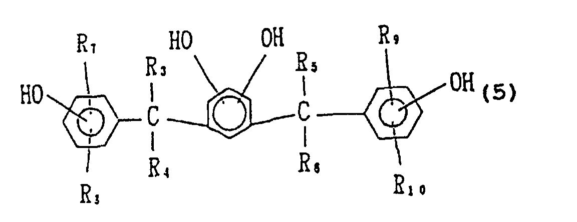
general formula (4) or (5) :
wherein R
3 to R
7 are as defined in the general formula (2).
wherein R
3 to R
10 may be the same or different and each represent
a hydrogen atom or methyl group.
Among the foregoing solid phenolic resins (component B1),
the pentafunctional solid phenolic resin can be in the form of
phenolic resin having a structure represented by the following
general formula (6):
wherein R
3 to R
10 are as defined in the general formula (5).
The foregoing solid phenolic resin to be used herein
preferably has a hydroxyl equivalent of from 30 to 260 g/eq and
a softening point of from 40°C to 100°C or a melting point of
from 50°C to 210°C, particularly a hydroxyl equivalent of from
50 to 110 g/eq and a softening point of from 60°C to 90°C or
a melting point of from 70°C to 190°C. The softening point can
be measured according to JIS K 7243.
The mixing proportion of the foregoing liquid epoxy resin
(component A1) and solid phenolic resin (component B1) is
preferably predetermined such that the amount of hydroxyl group
in the phenolic resin per equivalent of epoxy group in the
foregoing epoxy resin is from 0.6 to 1.4 equivalents, more
preferably from 0.7 to 1.1 equivalents.
In the first embodiment, the foregoing liquid epoxy resin
(component A1) and solid phenolic resin (component B1) to be
combined are preferably a bisphenol F type epoxy resin and a
polyfunctional solid phenolic resin from the standpoint of
fluidity, heat resistance and curability.
The second embodiment of the resin composition for
semiconductor encapsulation, which comprises a solid epoxy resin
(A2) as the epoxy resin (component A) and a liquid phenolic resin
(B2) as the phenolic resin (component B), will be further
described hereinafter.
The foregoing solid epoxy resin (component A2) is not
specifically limited so far as it stays solid at a temperature
of 25°C. Various epoxy resins may be used. Examples of the
epoxy resins employable herein include polyfunctional solid
epoxy resin, crystalline epoxy resin, bifunctional solid epoxy
resin, and triglycidyl isocyanurate. These solid epoxy resins
may be used singly or in combination of two or more thereof.
The term "polyfunctional solid epoxy resin" as used herein is
meant to indicate a solid epoxy resin having three or more epoxy
groups per molecule. Examples of the polyfunctional solid epoxy
resin employable herein include tetrafunctional naphthalene
type epoxy resin, and triphenylmethane type epoxy resin. The
term "crystalline epoxy resin" as used herein is meant to indicate
a solid epoxy resin which shows many crystalline peaks when
subjected to X-ray diffractometry, physically shows a sharp
melting point and exhibits a drastically lowered viscosity during
melting because there is little or no intermolecular mutual
interaction. Examples of the crystalline epoxy resin
employable herein include bisphenol type epoxy resin, biphenyl
type epoxy resin, and stilbene type epoxy resin. The term "solid
epoxy resin (component A2)" as used herein is meant to indicate
not only an epoxy resin which stays solid at 25°C when it is
used singly but also an epoxy resin component which is composed
of two or more of the epoxy resins and stays solid at 25°C.
Among the foregoing solid epoxy resins (component A2),
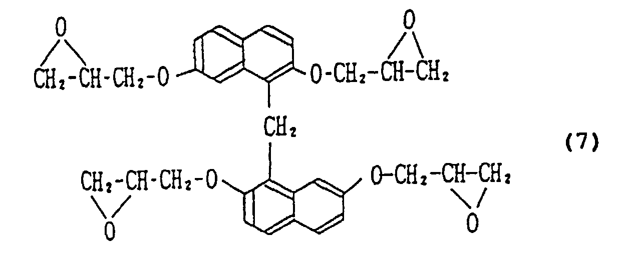
the tetrafunctional naphthalene type epoxy resin may be, e.g.,
Type EXA-4701 epoxy resin commercially available from DAINIPPON
INK & CHEMICALS, INC. Type EXA-4701 epoxy resin is represented
by the following structural formula (7):
Among the foregoing solid epoxy resins (component A2),
the triphenylmethane type epoxy resin may be, e.g., Type
EPPN-501HY epoxy resin commercially available from NIPPON KAYAKU
CO., LTD. Type EPPN-501HY epoxy resin is represented by the
following chemical formula (8):
wherein n represents 0 or a positive integer.
The foregoing solid epoxy resin to be used herein
preferably has an epoxy equivalent of from 140 to 250 g/eq and
a softening point of from 50°C to 100°C or a melting point of
from 45°C to 150°C, particularly an epoxy equivalent of from
150 to 220 g/eq and a softening point of from 60°C to 80°C or
a melting point of from 50°C to 130°C.
The liquid phenolic resin (component B2) to be used in
combination with the foregoing solid epoxy resin (component A2)
is not specifically limited so far as it acts as a curing agent
for the foregoing solid epoxy resin (component A2) and stays
liquid at a temperature of 25°C. Various phenolic resins can
be used. Examples of the liquid phenolic resin employable herein
include allylated phenol novolak, diallylated bisphenol A,
acetylated phenol, and diallylbisphenol F. These liquid
phenolic resins may be used singly or in combination of two or
more thereof. The term "liquid phenolic resin (component B2)"
as used herein is meant to indicate not only a phenolic resin
which stays liquid at 25°C when it is used singly but also a
phenolic resin component which is composed of two or more of
the phenolic resins and stays liquid at 25°C.
The foregoing liquid phenolic resin to be used herein
preferably has a hydroxyl equivalent of from 80 to 200 g/eq,
particularly from 100 to 170 g/eq.
The mixing proportion of the foregoing solid epoxy resin
(component A2) and liquid phenolic resin (component B2) is
preferably predetermined such that the amount of hydroxyl group
in the phenolic resin per equivalent of epoxy group in the
foregoing epoxy resin is from 0.7 to 1.4 equivalents, more
preferably from 0.9 to 1.1 equivalents.
In the second embodiment, the foregoing solid epoxy resin
(component A2) and liquid phenolic resin (component B2) to be
combined are preferably a tetrafunctional naphthalene type
epoxy resin and an allylated phenol novolak from the standpoint
of heat resistance and fluidity.
The third embodiment of the resin composition for
semiconductor encapsulation, which comprises a solid epoxy resin
(component A3) as the epoxy resin (component A) and a solid
phenolic resin (component B3) as the phenolic resin (component
B), will be further described hereinafter.
The foregoing solid epoxy resin (component A3) is not
specifically limited so far as it stays solid at a temperature
of 25°C. Various epoxy resins can be used. Examples of the
solid epoxy resin employable herein include polyfunctional solid
epoxy resin, crystalline epoxy resin, bifunctional solid epoxy
resin, triglycidyl isocyanurate, bisphenol F type epoxy resin,
and bisphenol A type epoxy resin. These solid epoxy resins may
be used singly or in combination of two or more thereof. The
term "polyfunctional solid epoxy resin" as used herein is meant
to indicate a solid epoxy resin having three or more epoxy groups
per molecule. Examples of the polyfunctional solid epoxy resin
employable herein include tetrafunctional naphthalene type
epoxy resin, triphenylmethane type epoxy resin,
dicyclopentadiene type epoxy resin, Techmore VG3101L (produced
by MITSUI CHEMICAL CORPORATION), and orthocresol novolak type
epoxy resin. The term "crystalline epoxy resin" as used herein
is meant to indicate a solid epoxy resin which shows many
crystalline peaks when subjected to X-ray diffractometry,
physically shows a sharp melting point and exhibits a drastically
lowered viscosity during melting because there is little or no
intermolecular mutual interaction. Examples of the crystalline
epoxy resin employable herein include bi sphenol type epoxy resin,
biphenyl type epoxy resin, and stilbene type epoxy resin. When
those having a melting point of 90°C or higher among these
crystalline epoxy resins are used, two or more of these
crystalline epoxy resins are preferably used for the reason that
the resulting fluidity at a temperature of 80°C or lower is
improved. The term "solid epoxy resin (component A3)" as used
herein is meant to indicate not only an epoxy resin which stays
solid at 25°C when it is used singly but also an epoxy resin
component which is composed of two or more of the epoxy resins
and stays solid at 25°C.
Among the foregoing solid epoxy resins (component A3),
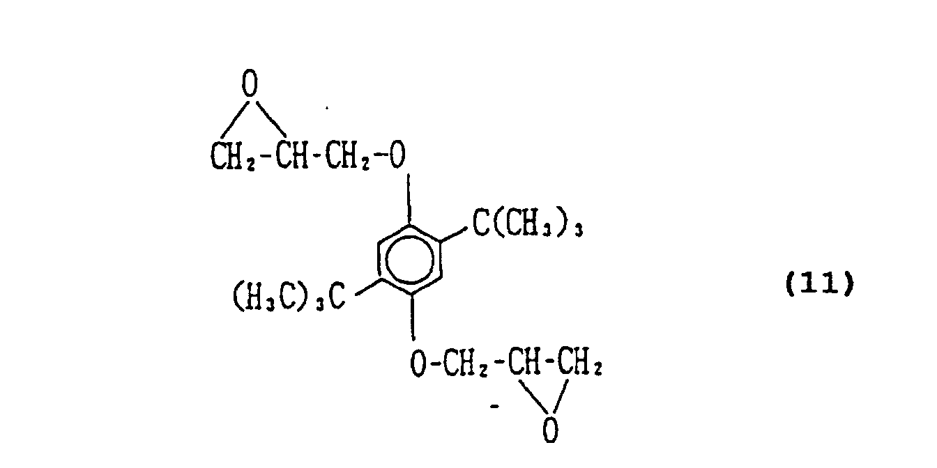
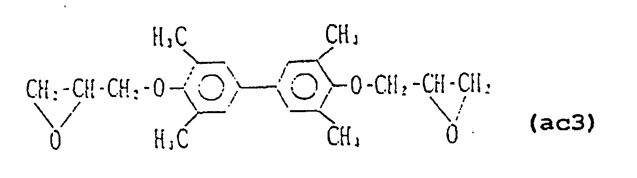
the crystalline epoxy resin may be, e.g., Type GK-4137 epoxy
resin (commercially available from NIPPON STEEL CORP.), Type
GK-5079 (commercially available from NIPPON STEEL CORP.), and
Type YDC-1312 (commercially available from Tohto Kasei Corp.).
Type GK-4137 epoxy resin is represented by the following chemical
formula (9). Type GK-5079 epoxy resin is represented by the
following chemical formula (10). Type YDC-1312 epoxy resin is
represented by the following chemical formula (11).
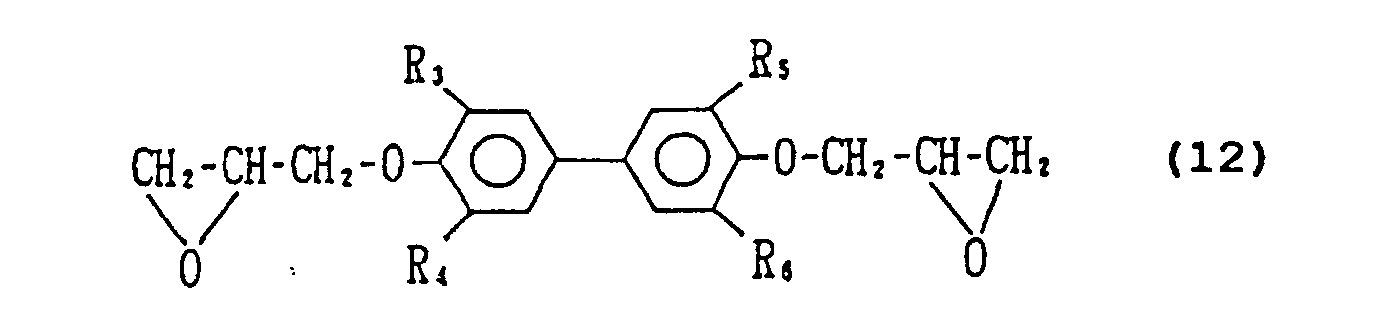
Among the foregoing crystalline epoxy resins, the biphenyl
type epoxy resin is represented by the following general formula
(12) :
wherein R
3 to R
6 may be the same or different and each represent
a hydrogen atom or C
1-5 alkyl group.
Examples of the C1-5 alkyl group represented by R3 to R6
in the foregoing general formula (12) include straight-chain
or branched lower alkyl group such as methyl group, ethyl group,
n-propyl group, isopropyl group, n-butyl group, isobutyl group,
sec-butyl group and tert-butyl group. R3 to R6 may be the same
or different.
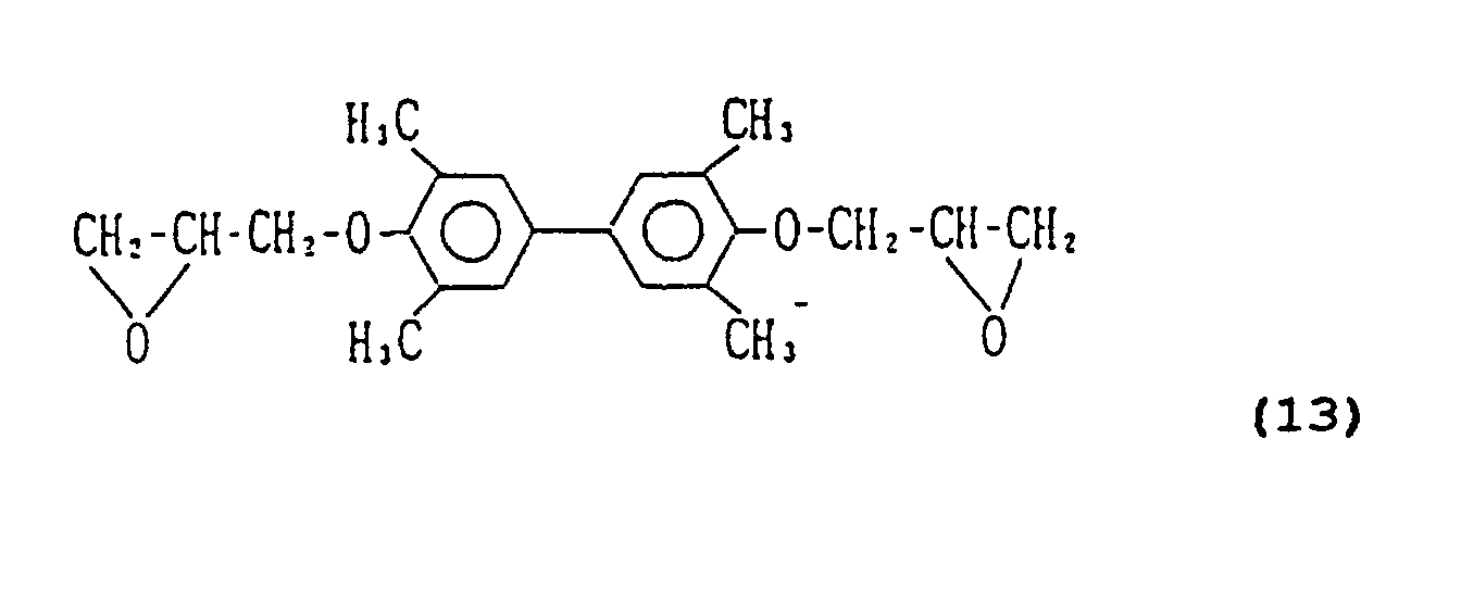
As the foregoing biphenyl type epoxy resin there can be
used a mixture of a biphenyl type epoxy resin having a structure
represented by the following general formula (13) wherein all
R
3 to R
6 are methyl group and a biphenyl type epoxy resin having
a structure represented by the following general formula (14)
wherein all R
3 to R
6 are hydrogen atom in almost the same amount:
The foregoing solid epoxy resin to be used as component
A3 preferably has an epoxy equivalent of from 140 to 270 g/eq
and a softening point of from 50°C to 100°C or a melting point
of from 40°C to 150°C, particularly an epoxy equivalent of from
150 to 220 g/eq and a softening point of from 60°C to 80°C or
a melting point of from 60°C to 130°C.
The foregoing solid phenolic resin (component B3) to be
used in combination with the solid epoxy resin (component A3)
is not specifically limited so far as it stays solid at a
temperature of 25°C. Various phenolic resins can be used.
These phenolic resins may be used in combination with acid
anhydride-based curing agents such as tetrahydrophthalic
anhydride, hexahydrophthalic anhydride,
methylhexahydrophthalic anhydride and phthalic anhydride,
amines, phthalic acids, etc. so far as the desired object of
the invention cannotbe impaired. Examples of the solidphenolic
resin (component B3) employable herein include polyfunctional
solid phenolic resin, bisphenols, terpenephenols,
terpenediphenols, dihydroxynaphthalenes, novolakphenol,
allylated phenol, acetylated phenol, and triphenylmethane type
phenolic resin. These solid phenolic resins maybe used singly
or in combination of two or more thereof. The term
"polyfunctional solid phenolic resin" as used herein is meant
to indicate a solid phenolic resin having at least one aromatic
ring containing two or more phenolic hydroxyl groups wherein
the number of phenolic hydroxyl groups per molecule is 3 or more
and there is contained two or more aromatic rings per molecule.
Examples of the polyfunctional solid phenolic resin employable
herein include trifunctional solid phenolic resin,
tetrafunctional solid phenolic resin, and pentafunctional solid
phenolic resin. The polyfunctional solid phenolic resin, if
used, preferably has a number-average molecular weight of 450
or less. The term "solid phenolic resin (component B3)" as used
herein is meant to indicate not only a phenolic resin which stays
solid at 25°C when it is used singly but also a phenolic resin
component which is composed of two or more of the phenolic resins
and stays solid at 25°C.
Among the foregoing solid phenolic resins (component B3),
the trifunctional solid phenolic resin may be, e.g., a phenolic
resin having a structure represented by the following general
formula (15) or (16):
wherein R
7 to R
11 may be the same or different and each represent
a hydrogen atom or methyl group.
wherein R
7 to R
11 are as defined in the general formula (15).
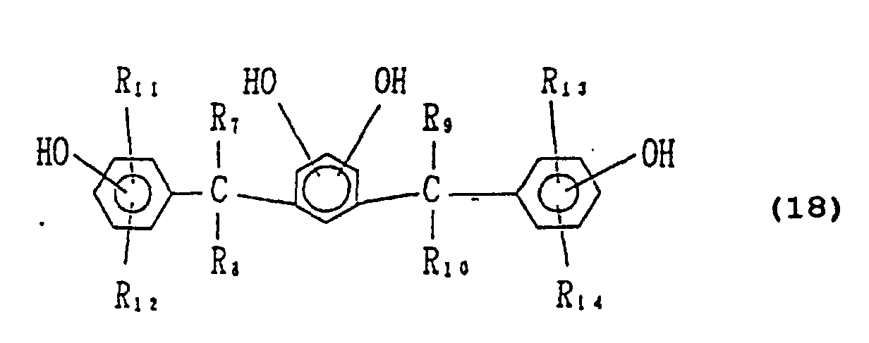
Among the solid phenolic resins (component B3), the
tetrafunctional solid phenolic resin can be, e.g., a phenolic
resin having a structure represented by the following general
formula (17) or (18):
wherein R
7 to R
11 are as defined in the general formula (15).
wherein R
7 to R
14 may be the same or different and each represent
a hydrogen atom or methyl group.
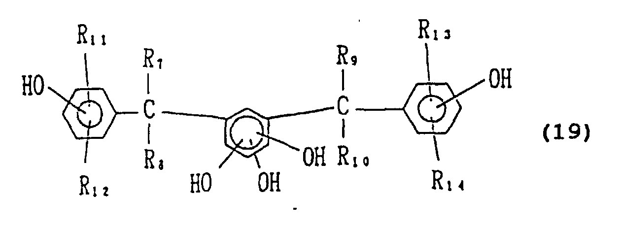
Among the solid phenolic resins (component B3), the
pentafunctional solid phenolic resin can be, e.g., a phenolic
resin having a structure represented by the following general
formula (19):
wherein R
7 to R
14 are as defined in the general formula (18).
The foregoing solid phenolic resin to be used as the
component B3 preferably has a hydroxyl equivalent of from 30
to 260 g/eq and a softening point of from 40°C to 100°C or a
melting point of from 50°C to 210°C, particularly a hydroxyl
equivalent of from 50 to 110 g/eq and a softening point of from
60°C to 90°C or a melting point of from 70°C to 190°C.
The mixing proportion of the foregoing solid epoxy resin
(component A3) and solid phenolic resin (component B3) is
preferably predetermined such that the amount of hydroxyl group
in the phenolic resin per equivalent of epoxy group in the
foregoing epoxy resin is from 0.6 to 1.4 equivalents, more
preferably from 0.7 to 1.1 equivalents.
The foregoing solid epoxy resin (component A3) and solid
phenolic resin (component B3) to be combined are preferably a
crystalline epoxy resin [particularly Type GK-4137 (produced
by NIPPON STEEL CORP. ] and a polyfunctional solid phenolic resin
or tetrafunctional naphthalene type epoxy resin or
triphenylmethane type epoxy resin and a bifunctional bisphenol
resin from the standpoint of curability, heat resistance and
fluidity.
The resin composition for semiconductor encapsulation of
the invention comprises a latent curing accelerator (component
C) and an inorganic filler (component D) incorporated therein
as essential components in combination with the various epoxy
resins and phenolic resins according to the first to third
embodiments.
When incorporated in the resin composition for
semiconductor encapsulation, the foregoing latent curing
accelerator (component C) acts to cause the resin composition
to show a viscosity increase of 10 times or less after 72 hours
of aging in a 50°C atmosphere (viscosity measured at 80°C). An
example of the latent curing accelerator is a microcapsule type
curing accelerator having a core-shell structure in which a core
portion made of one or more selected from various curing
accelerators is covered by a shell portion comprising as a main
component a polymer having a structural unit represented by the
following general formula (1) wherein the reactive amino group
present in the shell portion is blocked. The resin composition
for semiconductor encapsulation comprising such a microcapsule
type curing accelerator incorporated therein exhibits extremely
prolonged pot life and thus is excellent particularly in storage
stability. Even when the use of an ordinary curing accelerator
in a small amount causes the resin composition to show a viscosity
increase of 10 times or less, normally 1 to 3 times, the curing
accelerator is regarded as a latent curing accelerator.
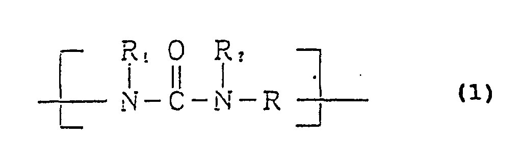
wherein R represents a divalent or trivalent organic group; and
R
1 and R
2, which may be the same or different, each represent
a hydrogen atom or monovalent organic group.
The curing accelerator to be encapsulated as a core portion
in the foregoing microcapsule type curing accelerator is not
specifically limited so far as it acts to accelerate curing
reaction. Known curing accelerators can be used. Those which
stay liquid at room temperature are suitable from the standpoint
of workability in microencapsulation or the characteristics of
the resulting mocrocapsules. The term "liquid at room
temperature" as used herein is meant to indicate that the curing
accelerator stays liquid at room temperature (25°C) itself or
the curing accelerator stays solid at room temperature but can
be liquefied by dissolving or dispersing in an arbitrary organic
solvent.
Examples of the curing accelerator to be encapsulated
include amine-based curing accelerator, imidazole-based curing
accelerator, phosphorus-based curing accelerator, and
phosphorus-boron-based curing accelerator. Specific examples
of these curing accelerators include alkyl-substituted
guanidines such as ethylguanidine, trimethylguanidine,
phenylguanine and diphenylguanidine, 3-substituted
phenyl-1,1-dimethylureas such as
3-(3,4-dichlorophenyl)-1,1-dimethylurea,
3-phenyl-1,1-dimethylurea and
3-(4-chlorophenyl)-1,1-dimethylurea,
3-phenyl-1,1-dimethylurea and
3-(4-chlorophenyl)-1,1-dimethylurea, imidazolines such as
2-methylimidazoline, 2-phenylimidazoline,
2-undecylimidazoline and 2-heptadecylimidazoline,
monoaminopyridines such as 2-aminopyridine, amineimides such
as N,N-dimethyl-N-(2-hydroxy-3-allyloxypropyl)amine-N'-lactamide,
organic phosphorus-based compounds such as
ethylphosphine, propylphosphine, butylphosphine,
phenylphosphine, trimethylphosphine, triethylphosphine,
tributylphosphine, trioctylphosphine, triphenylphosphine,
tricyclohexylphosphine, triphenylphosphine/triphenylborane
complex and tetraphenylphosphonium tetraphenylborate, and
diazabicycloalkenes such as 1,8-diazabicyclo[5,4,0]
undecene-7 and 1,4-diazabicyclo[2,2,2]octane. These curing
accelerators may be used singly or in combination of two or more
thereof. Preferred among these curing accelerators are
imidazole-based compounds and organic phosphorus-based
compounds from the standpoint of ease in production of curing
accelerator-containing microcapsules and handling.
The polymer comprising as a main component a polymer having
a structural unit represented by the foregoing general formula
(1) can be obtained by the polyaddition reaction of
polyisocyanates with polyvalent amines or the reaction of
polyisocyanates with water.
As the foregoing polyvalent isocyanates there can be used
any compounds having two or more isocyanate groups per molecule.
Specific examples of these polyvalent isocyanates include
diisocyanates such as m-phenylenediisocyanate,
p-phenylenediisocyanate, 2,4-tolylenediisocyanate,
2,6-tolylenediisocyanate, naphthalene-1,4-diisocyanate,
diphenylmethane-4,4'-diisocyanate,
3,3'-dimethoxy-4,4'-biphenyldiisocyanate,
3,3'-dimethyldiphenylmethne-4,4'-diisocyanate,
xylylene-1,4-diisocyanate, 4,4'-diphenylpropanediisocyanate,
trimethylenediisocyanate, hexamethylenediisocyanate,
propylene-1,2-diisocyanate, butylene-1,2-diisocyanate,
cyclohexylene-1,2-diisocyanate and
cyclohexylene-1,4-diisocyanate, triisocyanates such as
p-phenylenediisothiocyanate, xylylene-1,4-diisothiocyanate
and ethylidinediisothiocyanate, tetraisocyanates such as
4,4'-dimethyldiphenylmethane-2,2',5,5'-tetraisocyanate,
adduct of hexamethylenediisocyanate with hexanetriol, adduct
of 2,4-tolylenediisocyanate with Brenzcatechol, adduct of
tolylenediisocyanate with hexanetriol, adduct of
tolyenediisocyanate with trimethylolpropane, adduct of
xylylenediisocyanate with trimethylolpropane, adduct of
hexamethylenediisocyanate with trimethylolpropane, and
isocyanate prepolymers such as trimer of aliphatic polyvalent
isocyanate such as triphenyldimethylenetriisocyanate,
tetraphenyltrimethylene tetraisocyanate,
pentaphenyltetramethylene pentaisocyanate, lysine isocyanate
and hexamethylene diisocyanate. These compounds may be used
singly or in combination of two or more thereof.
Preferred among the foregoing polyvalent isocyanates are
isocyanate prepolymers represented by polymethylene polyphenyl
isocyanates such as adduct of tolylene diisocyanate and
trimethylol propane, adduct of xylylene diisocyanate and
trimethylolpropane and triphenyldimethylene triisocyanate from
the standpoint of film-forming properties in
microencapsulization and mechanical strength.
On the other hand, as the polyvalent amines to be reacted
with the polyvalent isocyanates there can be used any compounds
having two or more amino groups per molecule. Specific examples
of these compounds employable herein include diethylenetriamine,
triethylenetetramine, tetraethylene pentamine,
1,6-hexamethylenediamine, 1,8-octamethylene diamine,
1,12-dodecamethylenediamine, o-phenylenediamine,
m-phenylenediamine, p-phenylenediamine, o-xylylenediamine,
m-xylylenediamine, p-xylylenediamine, menthanediamine,
bis (4-amino-3-methylcyclohexyl)methane, isophoronediamine,
1,3-diaminocyclohexane, and spiroacetal-based diamine. These
compounds may be used singly or in combination of two or more
thereof.
The reaction of the polyvalent isocyanates with water
causes hydrolyzation of the polyvalent isocyanates resulting
in the production of an amine that is then reacted with unreacted
isocyanate groups (so-called self-polyaddition reaction) to
produce a polymer comprising as a main component a polymer having
a structural unit represented by the general formula (1).
As the polymer constituting the shell portion (wall
membrane) there may be used a polyurethane-polyurea having a
urethane bond in common with each other produced from the
polyvalent isocyanate and a polyvalent alcohol in combination.
As the foregoing polyvalent alcohol there can be used any
of aliphatic alcohol, aromatic alcohol and alicyclic alcohol.
Examples of the polyvalent alcohol employable herein include
catechol, resorcinol, 1,2-dihydroxy-4-methylbenzene,
1,3-dihydroxy-5-methylbenzene,
3,4-dihydroxy-1-methylbenzene,
3,5-dihydroxy-1-methylbenzene, 2,4-dihydroxyethylbenzene,
1,3-naphthalenediol, 1,5-napthalenediol, 2,7-naphthalenediol,
2,3-naphthalenediol, o,o'-biphenol, p,p'-biphenol, bisphenol
A, bis-(2-hydroxyphenyl)methane, xylylenediol, ethylene glycol,
1,3-propylene glycol, 1,4-butylene glycol, 1,5-pentanediol,
1,6-hexanediol, 1,7-heptanediol, 1,8-octanediol,
1,1,1-trimethylolpropane, hexanetriol, pentaerythritol,
glycerin, and sorbitol. These compounds may be used singly or
in combination of two or more thereof.
The foregoing microcapsule type curing accelerator can
be prepared through, e.g., the following three steps.
[1st step]
The curing accelerator as a core component is dissolved
or finely dispersed in a polyvalent isocyanate as a raw material
of wall (shell) to form an oil phase. Subsequently, the oil
phase thus formed is dispersed in the aqueous medium (aqueous
phase) containing a dispersion stabilizer in the form of oil
drop to prepare an O/W (oil phase/aqueous phase) emulsion.
Subsequently, in the O/W emulsion was dissolved a polyvalent
amine to cause interfacial polymerization of the polyvalent amine
with the polyvalent isocyanate in the oil phase to initiate
polyaddition reaction. Alternatively, the O/W emulsion is
heated so that the polyvalent isocyanate in the oil phase reacts
with water at the interface with the aqueous phase to produce
an amine that subsequently initiate self-polyaddition reaction.
Thus, microcapsules comprising as a shell portion (wall membrane)
a polyurea-based polymer, preferably a polyurea having a
structural unit represented by the general formula (1) are
prepared to obtain a microcapsule dispersion.
On the other hand, when a solid curing accelerator is
dissolved in an organic solvent to form a core component, an
S/O/W (solidphase/oil phase/aqueous phase) emulsion is obtained.
In this type of an emulsion, the curing accelerator is lipophilic.
A hydrophilic curing accelerator can be difficultly formed into
this type of an emulsion. In this case, however, the solubility
of the curing accelerator can be properly adjusted to form an
O/O (oil phase/oil phase) emulsion or S/O/O (solid phase/oil
phase/oil phase) emulsion which then undergoes interfacial
polymerization.
The organic solvent for dissolving the curing accelerator
therein is not specifically limited so far as it stays liquid
at room temperature. In practice, however, one which does not
dissolve the shell portion (wall membrane) therein needs to be
selected. Specific examples of the organic solvent employable
herein include organic solvents such as ethyl acetate, methyl
ethyl ketone, acetone, methylene chloride, xylene, toluene and
tetrahydrofuran, and oils such as phenylxylylethane and
dialkylnaphthalene.
[2nd step]
In the microcapsule dispersion obtained at the 1st step
is then dissolved or dispersed a blocking agent. In this
procedure, the addition of the blocking agent can be effected
after the removal of the dispersion stabilizer or unreacted amine
from the aqueous phase by centrifugal separation or the like
to advantage.
[3rd step]
The microcapsule dispersion which has been subjected to
blocking of amino group with a blocking agent at the 2nd step
can be subjected to centrifugal separation, filtration or the
like to remove excessive blocking agent, and then dried to prepare
a powdered microcapsule type curing accelerator.
Examples of the dispersion stabilizer to be added to the
aqueous medium (aqueous phase) at the 1st step include
water-soluble high molecular compounds such as polyvinyl alcohol
and hydroxymethyl cellulose, and surface active agents such as
anionic surface active agent, nonionic surface active agent and
cationic surface active agent. Alternatively, hydrophilic
inorganic colloidal materials such as colloidal silica and
viscous mineral may be used. The amount of such a dispersion
stabilizer to be added is preferably predetermined to be from
0.1 to 10% by weight based on the weight of the aqueous phase.
The blocking agent to be used at the 2nd step is not
specifically limited so far as it is a compound reactive with
amino group. Examples of such a compound employable herein
include compounds which react with amino group to form a covalent
bond such as epoxy compound, aldehyde compound, acid anhydride,
ester compound and isocyanate. Further examples of such a
compound include acidic compounds which undergo neutralization
reaction with amino group to form a salt such as organic carboxylic
acids (e.g., acetic acid, formic acid, lactic acid, oxalic acid
and succinic acid, organic sulfonic acids such as
p-toluenesulfonic acid, 2-naphthalenesulfonic acid and
dodecylbenzenesulfonic acid), phenol compounds, inorganic
acids such as boric acid, phosphoric acid, nitric acid, nitrous
acid and hydrochloric acid, and solid materials having an acidic
surface (e.g., silica, aerogil). Preferred among these
compounds are the acidic compounds, which can be used to
effectively block the amino group present on and inside the wall
membrane. Particularly preferred among these acidic compounds
are formic acid and organic sulfonic acids.
The foregoing blocking agent is added in an amount
equimolecular with the amino group present on and inside the
wall membrane. In practical, when as the blocking agent there
is used an acidic compound, the acidic material (acidic compound)
is added to the dispersion which has just been subjected to
microcapsulization (interfacial polymerization) so that the pH
value of the dispersion is adjusted from basicity to acidity,
preferably a pH of 2 to 5. Thereafter, the dispersion may be
subjected to centrifugal separation, filtration or the like to
remove excessive acidic compound.
In the process for the production of a microcapsule type
curing accelerator comprising the foregoing 1st to 3rd steps,
the 2nd step may also involve the passing of the microcapsule
dispersion through an acidic cation exchange column by which
the unreacted free amine can be removed or the remaining amino
group can be neutralized.
The average particle diameter of the microcapsule type
curing accelerator thus obtained is not specifically limited.
In practice, however, it is preferably predetermined to a range
of from 0.05 to 500 µm, more preferably from 0.1 to 30 µm from
the standpoint of uniformity in dispersion. The shape of the
microcapsule type curing accelerator is preferably sphere but
may be ellipsoid. In the case where the microcapsules are not
uniform in particle diameter, e.g., where the microcapsules are
ellipsoidal or flat rather than spherical, the value obtained
by simply averaging the longest diameter and the shortest
diameter is defined as average particle diameter.
The amount of the curing accelerator to be encapsulated
in the microcapsule type curing accelerator is preferably
predetermined to be from 10 to 95% by weight, particularly from
30 to 80% by weight based on the total amount of microcapsules.
In other words, when the amount of the curing accelerator to
be encapsulated falls below 10% by weight, the curing reaction
time is too long to give sufficient reactivity. On the contrary,
when the amount of the curing accelerator to be encapsulated
exceeds 95% by weight, the thickness of the resulting wall
membrane is too small to provide the core portion (curing agent)
with sufficient isolatability and mechanical strength.
The ratio of the thickness of the shell portion (wall
membrane) to the particle diameter of the microcapsule type
curing accelerator is preferably predetermined to a range of
from 3 to 25%, particularly from 5 to 25%. In other words, when
the foregoing ratio falls below 3%, the resulting microcapsules
cannot be provided with a sufficient mechanical strength against
the shear developed at the kneading step during the production
of epoxy resin composition. On the contrary, when the foregoing
ratio exceeds 25%, there is a tendency that the curing accelerator
encapsulated is insufficiently released.
The amount of the latent curing accelerator (component
C) to be incorporated is preferably predetermined to a range
of from 0.1 to 40 parts by weight (hereinafter abbreviated as
"parts"), particularly from 5 to 20 parts based 100 parts of
the foregoing embodiments of phenolic resin (components B1 to
B3). In other words, when the amount of the latent curing
accelerator to be incorporated falls below 0.1 parts, the curing
rate is so low that the resulting strength is liable to be lowered.
On the contrary, when the amount of the latent curing accelerator
to be incorporated exceeds 40 parts, the curing rate is so high
that the fluidity is liable to be impaired. The use of the
above-described latent curing accelerator generally provides
a resin composition showing a viscosity increase of 10 times
or less after 72 hours of aging in a 50°C atmosphere (viscosity
measured at 80°C).
In the invention, as the latent curing accelerator to be
used as component C there may be used a commercially available
microcapsule type curing accelerator besides the curing
accelerator-containing microcapsules so far as the desired
object cannot be impaired. Examples of these commercially
available microcapsule type curing accelerators include
MCE-9957 (comprising as wall membrane methyl methacrylate;
produced by NIPPON KAYAKU CO. , LTD.), and Novacure produced by
Asahi Ciba Co., Ltd. (HX-3748, 3741, 3742, HX-3921HR, HX-3941HP).
Even curing accelerators other than microcapsule type curing
accelerator may be used such as those having a reduced catalytic
activity such as dicyan diamide and Fujicure FXR-1030 and
FXE-1000 produced by Fuji Chemical Industry Corp. or if they
are ordinary curing accelerators and added in a small amount
to give a reduced catalyst activity.
The inorganic filler (component D) to be used as the
component C is not specifically limited. Various inorganic
fillers maybe used. Examples of these inorganic fillers include
silica, clay, gypsum, calcium carbonate, barium sulfate, alumina
oxide, beryllium oxide, silicon carbide, silicon nitride, and
aerogil. These compounds may comprise an
electrically-conductive particulate material such as nickel,
gold, copper, silver, tin, lead and bismuth incorporated therein.
Preferred among these compounds is spherical silica powder,
particularly spherical fused silica powder. The average
particle diameter of the inorganic filler is preferably from
0.01 to 60 µm, more preferably from 0.1 to 15 µm. The term
"spherical" as used herein is meant to indicate that the
sphericity is 0.85 or more on the average as measured by a Type
FPIA-100 flow type particle image analyzer (produced by SYSMEX
INC.) .
The content of the inorganic filler (component D) is
preferably predetermined to a range of from 15 to 85%,
particularly from 50 to 80% based on the total weight of the
resin composition for semiconductor encapsulation. In other
words, when the content of the inorganic filler falls below 15%
by weight, the resulting resin composition for semiconductor
encapsulation tends to exhibit a reduced viscosity at 25°C and
thus undergoes sedimentation of inorganic filler during storage
or exhibit a high hygroscopicity and hence a deteriorated
reliability in humidity resistance. On the contrary, when the
content of the inorganic filler exceeds 85%, the resulting resin
composition for semiconductor encapsulation tends to exhibit
a reduced fluidity and hence deteriorated dischargeability and
coatability.
Further, the resin composition for semiconductor
encapsulation of the invention may comprise other additives
incorporated therein besides the foregoing essential components
as necessary.
Examples of the other additives employable herein include
fire retardant,wax,leveling agent,anti-foaming agent, pigment,
dye, silane coupling agent, and titanate-based coupling agent.
Examples of the silane coupling agent employable herein include
γ-mercaptopropyl trimethoxysilane, γ-glycidoxypropyl methyl
diethoxysilane,
β-(3,4-epoxycyclohexyl)ethyltrimethoxysilane,
γ-methacryloxypropyl trimethoxysilane, and amino
group-containing silane. These silane coupling agents may be
used singly or in combination of two or more thereof.
Examples of the fire retardant employable herein include
novolak type bromated epoxy resin, and bromated bisphenol A type
epoxy resin, metallic compounds such as antimony trioxide,
antimony pen taoxide, magnesium hydroxide and aluminum hydroxide,
and phosphorus-based compounds such as red phosphorus and ester
phosphate. These fire retardants may be used singly or in
combination of two or more thereof.
Examples of the wax employable herein include a higher
fatty acid, a higher fatty acid ester, a higher fatty acid
calcium, and an amide-based compound. These waxes may be used
singly or in combination of two or more thereof.
The resin composition for semiconductor encapsulation of
the invention may comprise a silicone oil, silicone rubber,
synthetic rubber or reactive diluent incorporated therein
besides the above-described other additives to reduce the
resulting stress. The resin composition for semiconductor
encapsulation of the invention may comprise an ion trap agent
such as hydrotalcite and bismuth hydroxide for the purpose of
enhancing the reliability in the humidity resistance reliability
test.
The resin composition for semiconductor encapsulation of
the invention can be prepared, e.g., in the following manner.
In some detail, the foregoing components A to D and optionally
other additives are mixed, and then kneaded under heating in
a kneader such as universal agitator so that it is melt-mixed.
Subsequently, the mixture is cooled to room temperature (approx.
25°C) to produce the desired resin composition for semiconductor
encapsulation. In order to adjust the fluidity of the resin
composition for semi conductor encapsulation, an organic solvent
may be added. Examples of the organic solvent employable herein
include toluene, xylene, methyl ethyl ketone (MEK), acetone,
and diacetone alcohol. These organic solvents maybe used singly
or in combination of two or more thereof.
The viscosity of the resin composition for semiconductor
encapsulation thus obtained must be predetermined to a range
of from 7,000 poise or more at 25°C and 5,000 poise or less at
80°C, particularly 7,000 poise or more at 25°C and 3,000 poise
or less at 80°C. The lower limit of the viscosity of the resin
composition for semiconductor encapsulation at 80°C is generally
1.0 poise. In other words, when the viscosity of the resin
composition for semiconductor encapsulation falls below 7,000
poise at 25°C and exceeds 5,000 poise at 80°C, the resulting
resin composition for semiconductor encapsulation exhibits
deteriorated storage stability, dischargeability and
coatability and thus cannot satisfy the desired requirements.
The viscosity of the resin composition for semiconductor
encapsulation at 25°C and 80°C can be measured by an E type
viscometer as follows.
[Viscosity at 25°C]
For the measurement of viscosity at 25°C, a Type REBOU
viscometer comprising a cone rotor having a size of 3° and R7.7
produced by Toki Sangyo Co., Ltd. was used. The sample was
pretreated at a cone rotor rotary speed of 1 rpm for 1 minute
at 25°C, and then allowed to stand at 0.1 rpm for 10 minutes
at 25°C before measurement.
[Viscosity at 80°C]
For the measurement of viscosity at 80°C, a Type RE80R
viscometer produced by Toki Sangyo Co., Ltd. was used. For the
sample having a viscosity of less than 1,000 poise, a cone rotor
having a size of 3° x R14 was used. For the sample having a
viscosity of 1,000 poise or more, a cone rotor having a size
of 3° x R7.7 was used. The sample was pretreated at a cone rotor
rotary speed of 1 rpm for 1 minute at 80°C, and then allowed
to stand at 0.5 rpm for 10 minutes at 80°C before measurement.
The production of a semiconductor device from the resin
composition for semiconductor encapsulation of the invention
is accomplished by various known methods. In mounting by flip
chip, COB, graph top, cavity fill, etc., the resin composition
for semiconductor encapsulation which has been heated (to a
temperature of from about 40°C to 90°C, preferably from about
60°C to 80°C) is supplied by means of a dispenser so that the
semiconductor element is potted. The resin composition is then
heated and cured to form an encapsulating resin layer. Thus,
a semiconductor device can be produced. Alternatively, a solid
or semi-solid resin composition for semiconductor encapsulation
may be directly adhered or applied to the semiconductor element,
etc., and then heated and cured to form an encapsulating resin
layer. Thus, a semiconductor device can be produced. The
mounting may be effected in vacuo.
Among the foregoing processes for the production of a
semiconductor device, flip chip mounting will be further
described hereinafter with reference to side fill encapsulation
process, press bump encapsulation process and printing
encapsulation process.
[Side fill encapsulation process]
A wiring circuit board having semiconductor elements
provided thereon with a plurality of connecting electrode
portions interposed therebetween is prepared. The gap between
the wiring circuit board and semiconductor elements which have
been previously heated (to a temperature of from about 40°C to
130°C, preferably from 60°C to 100°C) is then filled with the
resin composition for semiconductor encapsulation which has been
heated (to a temperature of from about 40°C to 90°C, preferably
from about 60°C to 80°C) and injected by means of a dispenser.
The resin composition thus injected is then heated and cured
to form an encapsulating resin layer. In this manner, a
semiconductor device can be produced by flip chip mounting.
Alternatively, a solid or semi-solid resin composition
for semiconductor encapsulation which has not previously been
heated may be directly applied onto the semiconductor elements
or to the area in the vicinity thereof, and then heated and cured
to form an encapsulating resin layer in the gap between the
semiconductor elements and the wiring circuit board.
The production of a semiconductor by side fill
encapsulation process may be effected in vacuo. As the apparatus
for the production of such a semiconductor device in vacuo there
may be used a Type MBC-V Series produced by Musashi Engineering
Co., Ltd. The foregoing production of a semiconductor device
in vacuo may be accomplished by differential pressure filling
method which comprises filling of the gap between the wiring
circuit board and the semiconductor-elements in vacuo with the
resin composition for semiconductor encapsulation which has been
injected by means of a dispenser and subsequent filling the gap
with the resin composition at atmospheric pressure.
[Press bump encapsulation process]
The resin composition for semiconductor encapsulation
which has been heated (to a temperature of from about 40°C to
90C, preferably from 60°C to 80°C) is applied onto the wiring
circuit board by means of a dispenser so that the semiconductor
elements are potted. Thereafter, press bump connection process
using a flip chip bonder or the like is effected to carry out
the electrical connection between the semiconductor elements
and the wiring circuitboard and the formation of an encapsulating
resin layer at the same time. In this manner, a semiconductor
device can be produced by flip chip mounting.
Alternatively, a solid or semi-solid resin composition
for semiconductor encapsulation which has not previously been
heated may be directly applied to the semiconductor elements
or wiring circuit board, followed by press bump connection
process. In this manner, the connection between the
semiconductor elements and the wiring circuit board and the
formation of an encapsulating resin layer can be effected at
the same time.
The production of a semiconductor device by press bump
encapsulation process may be effected in vacuo.
Instead of potting by means of a dispenser, printing may
be effected to apply the resin composition if possible, followed
by press bump connection process by flip chip bonder or the like
which effects the electrical connection between the
semiconductor elements and the wiring circuit board and the
formation of an encapsulating resin layer at the same time. In
the application by printing, the printing atmosphere may be
entirely heated or the mask or squeegee may be partly heated
(to a temperature of from about 40°C to 100°C).
[Printing encapsulation process]
A wiring circuit board having semiconductor elements
provided thereon with a plurality of connecting electrode
portions interposed therebetween is prepared. The resin
composition for semiconductor encapsulation which has been
heated (to a temperature of from about 40°C to 90°C, preferably
from about 60°C to 80°C) is then dropped into the gap between
the wiring circuit board and semiconductor elements which has
previously been heated (to a temperature of from about 40°C to
130°C, preferably from about 60°C to 100°C) by means of a dispenser
so that printing encapsulation is effected to form an
encapsulating resin layer. In this manner, a semiconductor
device can be produced by flip chip mounting.
The printing encapsulation process is preferably
accomplished by the use of a Type VPE-100 Series vacuum printing
encapsulation apparatus using vacuum differential pressure
(produced by Toray Engineering Co. , Ltd.) because air bubbles
can hardly enter into the encapsulating resin layer.
Alternatively, a solid or semi-solid resin composition
for semiconductor encapsulation which has not previously been
heated may be directly applied to a stage or squeegee so that
printing encapsulation can be effected.
On the other hand, among the foregoing processes for the
production of a semiconductor device, the cavity fill process
for the production of a semiconductor device will be further
described hereinafter.
A wiring circuit board having semiconductor elements
provided thereon in such an arrangement that the semiconductor
elements are electrically connected thereto through a bonding
wire or the like is prepared. The resin composition for
semiconductor encapsulation which has been heated (to a
temperature of from about 40°C to 90°C, preferably from about
60°C to 80°C) is then applied to the wiring circuit board and
semiconductor elements which has previously been heated (to a
temperature of from about 40°C to 130°C, preferably from about
60°C to 100°C) by means of a dispenser so that the semiconductor
elements are potted. The resin composition is then heated and
cured so that an encapsulating resin layer is formed to
encapsulate the semiconductor elements. In this manner, a
cavity fill type of semiconductor device can be produced.
Alternatively, a solid or semi-solid resin composition
for semiconductor encapsulation which has not previously been
heated may be directly adhered or applied to the semiconductor
elements, and then heated and cured to form an encapsulating
resin layer in such an arrangement that the semiconductor
elements are encapsulated.
The production of a semiconductor device by the foregoing
encapsulation method may be effected in vacuo. As the apparatus
for the production of such a semiconductor device in vacuo there
may be used a Type MBC-V Series produced by Musashi Engineering
Co., Ltd.
Other processes for the production of a semiconductor
device will be further described hereinafter. A wiring circuit
board having semiconductor elements provided thereon in such
an arrangement that the semiconductor elements are electrically
connected thereto through a bonding wire or the like is prepared.
The resin composition for semiconductor encapsulation which has
been heated (to a temperature of from about 40°C to 90°C,
preferably from about 60°C to 80°C) is then supplied on the wiring
circuit board and semiconductor elements which have previously
been heated (to a temperature of from about 40°C to 130°C,
preferably from 60°C to 100°C) by printing or the like, and then
heated and cured to form an encapsulating resin layer in such
an arrangement that the semiconductor elements are encapsulated.
In this manner, a cavity fill type of semiconductor device can
be produced.
The production of a semiconductor device by printing
encapsulation process may be effected in vacuo. In the procedure
of producing a semiconductor device in vacuo, printing
encapsulation in vacuo may be followed by the rise in the
atmospheric pressure that causes the removal of voids from the
resin composition for semiconductor encapsulation. Finish
printing may be then effected under these conditions.
The semiconductor device is then placed on a mounting board
(mother board) to produce a semiconductor product. In some
detail, the semiconductor device is mounted on the mounting board
(mother board) with a plurality of connecting electrode portions
being provided interposed therebetween and its wiring circuit
board being opposed to the mounting board. At the same time,
the gap between the mounting board and the semiconductor device
is filled with the resin composition for semiconductor
encapsulation of the invention which is then heated and cured
to form an encapsulating resin layer. In this manner, a
semiconductor product is produced.
The method for heating and curing the resin composition
for semiconductor encapsulation is not specifically limited.
In practice, however, a heating method using a convection dryer,
IR reflow furnace, hot plate or the like can be used.
Examples of the method for filling the gap between the
mounting board and the semiconductor device with the resin
composition for semiconductor encapsulation of the invention
include the same methods as described with flip chip mounting
among the processes for the production of a semiconductor device
mentioned above, i.e., side fill encapsulation process, press
bump encapsulation process, printing encapsulation process, etc.
The resin composition for semiconductor encapsulation may
comprise an electrically-conductive particulate material such
as nickel, gold, silver, copper, tin, lead and bismuth dispersed
therein to form ACF (Anisotropic Conductive Film) or ACP
(Anisotropic Conductive Paste) which is then used for flip chip
mounting. In other embodiments, the resin composition for
semiconductor encapsulation may be applied to the wiring circuit
board as a damming material or may be used as an adhesive for
bonding the wiring circuit board to the heat radiator or a
die-bonding agent.
The production of a semiconductor device comprising the
resin composition for semiconductor encapsulation of the
invention which has been provided on a semiconductor wafer or
matrix wiring circuit board can be accomplished by various known
methods.
The production of a semiconductor device will be described
with reference to the case where the resin composition for
semiconductor encapsulation of the invention is applied to a
semi conductor wafer having a plurality of semi conductor elements
with protruding electrode portions formed thereon. In some
detail, the resin composition for semiconductor encapsulation
which has been heated (to a temperature of from about 40°C to
90°C, preferably from about 60°C to 80°C) is applied to the
protruding electrode portion side of the semiconductor wafer
by means of a dispenser to form a resin layer made of the resin
composition for semiconductor encapsulation to a predetermined
thickness. The formation of a resin layer made of the resin
composition for semiconductor encapsulation to a predetermined
thickness is effected in such a manner that at least the forward
end of the protruding electrode portion is exposed to the exterior
of the resin layer. Subsequently, the semiconductor wafer
having a resin layer formed thereon is cut to produce a
semiconductor device.
The formation of a resin layer made of the resin composition
for semiconductor encapsulation can be carried out by printing
through an opening in the mask.
The resin layer thus formed may be in any state so far
as it is eventually thermoset. The heating and curing of the
resin layer may be effected before or after cutting of the
semiconductor wafer. -
On the other hand, the resin composition for semiconductor
encapsulation is supplied onto the whole of a plurality of
semiconductor elements mounted on a matrix wiring circuit board
having individual wiring circuits formed thereon to form a resin
layer in such an arrangement that the semiconductor elements
are encapsulated. Subsequently, the resin layer is thermoset
to encapsulate the plurality of semiconductor elements with the
resin composition. The plurality of semiconductor elements
thus encapsulated are then cut every semiconductor element to
produce semiconductor devices.
The resin layer thus formed may be in any state so far
as it is eventually thermoset. The heating and curing of the
resin layer may be effected before or after cutting of the
semiconductor elements.
As the method for forming the resin layer made of the resin
composition for semiconductor encapsulation there may be used
a method using a dispenser, a method involving printing through
an opening in the mask or the like similarly to the method
previously mentioned.
Alternatively, the resin composition for semiconductor
encapsulation is supplied onto the protruding electrode portion
side of a semiconductor wafer having a plurality of semiconductor
elements with protruding electrode portions formed thereon to
form a resin layer to a predetermined thickness. The
semiconductor wafer having a resin layer formed thereon is then
cut to individual semiconductor elements. Subsequently, the
wiring circuit board and the semiconductor elements are
contact-bonded to each other under heating with the resin layer
side of the semiconductor elements thus separated and the
plurality of wiring circuit boards being opposed to each other
so that they are electrically connected to each other. At the
same time, the resin layer is melted and cured to form an
encapsulating resin layer between the semiconductor elements
and the wiring circuit boards so that the semiconductor elements
are encapsulated. In this manner, a semiconductor device is
produced.
Alternatively, the resin composition for semiconductor
encapsulation is supplied onto a matrix wiring circuit board
having individual wiring circuits formed thereon to form a resin
layer. The wiring circuit board having a resin layer formed
thereon is then cut to individual wiring circuit boards.
Subsequently, semiconductor elements each provided with a
plurality of connecting electrode portions and the wiring circuit
boards thus separated are contact-bonded to each other under
heating with the connecting electrode portion side of the
semiconductor elements and the wiring circuit boards being
opposed to each other so that they are electrically connected
to each other. At the same time, the resin layer is melted and
cured to form an encapsulating resin layer between the
semiconductor elements and the wiring circuit boards so that
the semiconductor elements are encapsulated. In this manner,
a semiconductor device is produced.
As the method for forming the resin layer made of the resin
composition for semiconductor encapsulation there may be used
a method using a dispenser, a method involving printing through
an opening in the mask or the like similarly to the method
previously mentioned.
The present invention will be further described in the
following examples and comparative examples, but the present
invention should not be construed as being limited thereto.
(1) Examples and comparative examples of the first embodiment
of the resin composition for semiconductor encapsulation
(combination of a liquid epoxy resin and a solid phenolic resin)
will be described hereinafter.
The following various components were prepared prior to
these examples.
[Epoxy resin aa1]
Bisphenol F type epoxy resin (Epo Tohto YDF-8170, produced
by Tohto Kasei Co. , Ltd.; liquid at 25°C; epoxy equivalent: 158
g/eq)
[Epoxy resin aa2]
Bisphenol A type epoxy resin (DER-332, produced by The
Dow Chemical Company; liquid at 25°C; epoxy equivalent: 170 g/eq)
[Epoxy resin aa3]
Alicyclic epoxy resin (Celloxide 2021P, produced by DAISEL
CHEMICAL INDUSTRIES, LTD; liquid at 25°C; epoxy equivalent: 135
g/eq)
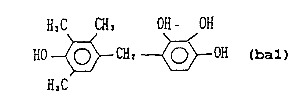
[Phenolic resin ba1]
Tetrafunctional phenolic resin represented by the
following chemical formula (ba1) (THD-2344, produced by Honshu
Chemical Industry Co., Ltd.; solid at 25°C; melting point: 187°C;
purity: 94%)
Pentafunctional phenolic resin represented by the
following chemical formula (ba2) (BisPG-26X, produced by Honshu
Chemical Industry Co., Ltd.; solid at 25°C; melting point: 182°C;
purity: 97.5%)
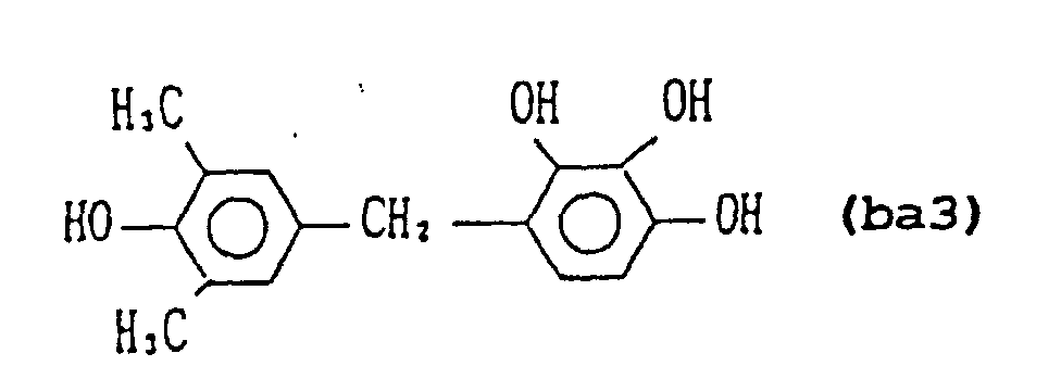
Tetrafunctional phenolic resin represented by the
following chemical formula (ba3) (MHD-2344, produced by Honshu
Chemical Industry Co., Ltd.; solid at 25°C; melting point: 156°C;
purity: 93.6%)
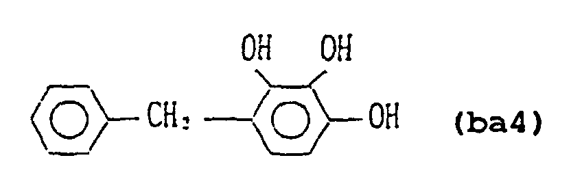
Trifunctional phenolic resin represented by the following
chemical formula (ba4) (HDM-234, produced by Honshu Chemical
Industry Co., Ltd.; solid at 25°C; melting point: 94°C; purity:
98%)
Solid phenolic resin represented by the following chemical
formula (ba5) (TrisP-RK, produced by Honshu Chemical Industry
Co., Ltd.; solid at 25°C; melting point: 95°C; purity: 89%)
Triphenylmethane type phenolic resin [MEH-7500 (3,4P),
produced by Meiwa Kasei Co., Ltd.; solid at 25°C; hydroxyl
equivalent: 101 g/eq; melting point: 110°C; 150°C viscosity:
3 to 4 poise]
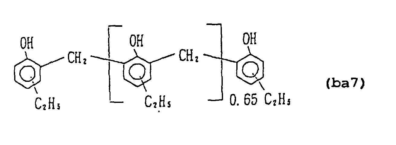
[Phenolic resin ba7]
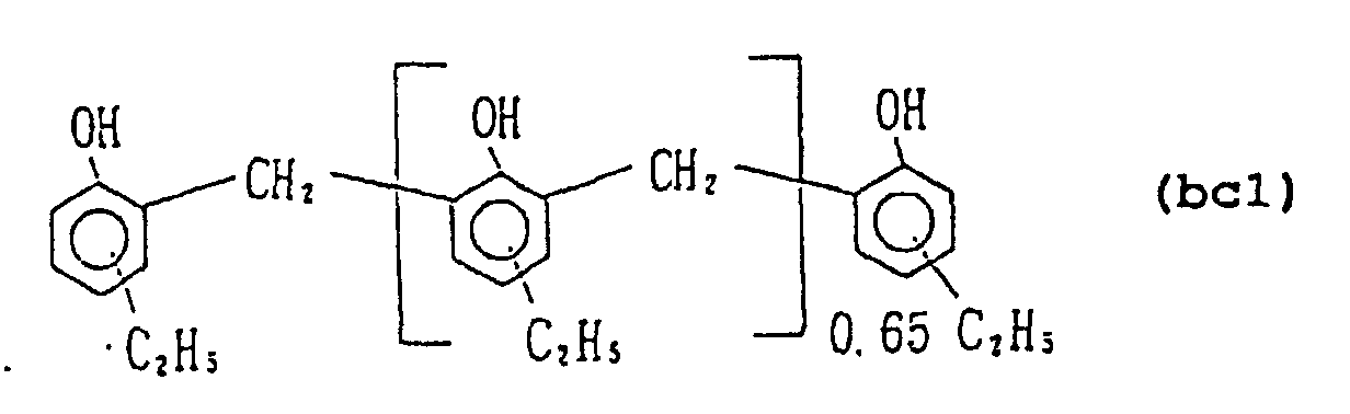
p-Ethylphenol resin represented by the following chemical
formula (ba7) (produced by Meiwa Kasei Co., Ltd.; solid at 25°C;
hydroxyl equivalent: 129 g/eq; melting point: 98°C)
Allylated phenol novolak (MEH-8005H, produced by Meiwa
Kasei Co. , Ltd.; liquid at 25°C; hydroxyl equivalent: 135 g/eq)
[Acid anhydride-based curing agent]
Methylhexahydrophthalic anhydride (methylated HHPA,
Rikacid MH-700, produced by New Japan Chemical Co., Ltd.)
[Curing accelerator c1]
A microcapsule type curing accelerator was prepared in
accordance with the method previously mentioned. In some detail,
11 parts of an adduct of 3 mols of xylylene diisocyanate and
1 mol of trimethylolpropane and 4.6 parts of an adduct of 3 mols
of tolylene diisocyanate and 1 mol of trimethylolpropane were
uniformly dissolved in a mixture of 7 parts of triphenyl phosphine
and 3.9 parts of ethyl acetate as curing accelerators to prepare
an oil phase. Separately, an aqueous phase comprising 100 parts
of distilled water and 5 parts of a polyvinyl alcohol was prepared.
To the aqueous phase thus prepared was then added the oil phase
prepared as above. The mixture was then subjected to
emulsification by means of a homomixer to form an emulsion. The
emulsion thus formed was then charged into a polymerization
reactor equipped with a reflux tube, an agitator and a dropping
funnel.
On the other hand, 10 parts of an aqueous solution
containing 3 parts of triethylenetetramine were prepared. The
aqueous solution thus prepared was then put into the dropping
funnel provided in the foregoing polymerization reactor. The
aqueous solution was dropped into the emulsion in the reactor
where interfacial polymerization took place at a temperature
of 70°C for 3 hours to obtain an aqueous suspension of microcapsule
type curing accelerator. Subsequently, the aqueous suspension
was subjected to centrifugal separation to remove the polyvinyl
alcohol, etc. from the aqueous phase. To the residue were then
added 100 parts of distilled water. The mixture was then
subjected to dispersion to obtain a suspension.
To the suspension was then added formic acid to adjust
the pH value of the system to 3. In this manner, a microcapsule
type curing accelerator in which the amino group present on and
inside the wall membrane had been blocked with formic acid was
prepared. The microcapsule type curing accelerator thus
obtained was repeatedly subjected to centrifugal separation and
rinsing, and then dried to isolate the microcapsule type curing
accelerator as a free-flowing powder. The average particle
diameter of the microcapsule type curing accelerator was 2 µm.
The ratio of the shell thickness to the particle diameter of
microcapsules was 15%. The encapsulated amount of
triphenylphosphine was 30% by weight based on the total amount
of the microcapsule type curing accelerator.
[Curing accelerator c2]
MCE-9957 produced by NIPPON KAYAKU CO., LTD.
[Curing accelerator c3]
2-Ethyl-4-methylimidazole (Curezol 2E4MZ, produced by
Shikoku Chemicals Corp.)
[Inorganic filler d1]
Spherical fused silica powder (SP-4B, produced by TONEN
CHEMICAL CORPORATION; average particle diameter: 5.0 µm)
[Inorganic filler d2]
Spherical fused silica powder (FB-48X, produced by DENKI
KAGAKU KOGYO K.K.; average particle diameter: 15 µm)
[Inorganic filler d3]
Spherical fused silica powder (SE-2100, produced by
Admatechs Co., Ltd.; average particle diameter: 0.56 µm)
EXAMPLES a1 - a12; COMPARATIVE EXAMPLES a1 - a4; CONVENTIONAL
EXAMPLES
The foregoing various components were mixed in proportions
set forth in Tables 1 to 3 below, and then kneaded in a universal
agitator so that they were melt-mixed. Subsequently, the
mixture was cooled to room temperature to prepare the desired
resin compositions for semiconductor encapsulation. The
kneading conditions were as follows.
[EXAMPLES a1 - a8; COMPARATIVE EXAMPLE a4]
The epoxy resin and the phenolic resin were charged into
the universal agitator where they were stirred at a temperature
of 150°C for 2 minutes to dissolve all the solid contents.
Subsequently, the temperature of the solution was lowered to
a range of from 90°C to 100°C. To the solution was then added
the inorganic filler. The mixture was then stirred for 10 minutes.
The mixture was then adjusted to a temperature of 75°C. To the
mixture was then added the curing accelerator. The mixture was
then stirred for 2 minutes for use.
[EXAMPLES a9 - a12; COMPARATIVE EXAMPLES a2, a3]
The epoxy resin and the phenolic resin were charged into
the universal agitator where they were then stirred at a
temperature of 110°C for 5 minutes to dissolve all the solid
contents. Subsequently, the temperature of the solution was
lowered to a range of from 90°C to 100°C. To the solution was
then added the inorganic filler. The mixture was then stirred
for 10 minutes. The mixture was then adjusted to a temperature
of 65°C. To the mixture was then added the curing accelerator.
The mixture was then stirred for 2 minutes for use.
[COMPARATIVE EXAMPLE a1; CONVENTIONAL EXAMPLE]
The epoxy resin, the phenolic resin or the acid anhydride
were charged into the universal agitator where they were then
stirred at a temperature of 80°C for 10 minutes. Thereafter,
the mixture was stirred with the inorganic filler at the same
temperature for 10 minutes. The temperature of the mixture was
then lowered to 50°C. To the mixture was then added the curing
accelerator. The mixture was then stirred for 2 minutes for
use.
| (Unit: parts) |
| | Example No. |
| | a1 | a2 | a3 | a4 | a5 | a6 |
| Epoxy resin | aa1 | 404 | 404 | 341 | 358 | 414 | 207 |
| aa2 | - | - | - | - | - | - |
| aa3 | - | - | - | - | - | - |
| Phenolic resin | ba1 | 93.9 | 93.9 | - | - | - | - |
| ba2 | 93.9 | 93.9 | 77 | 80.7 | 93 | 46.5 |
| ba3 | - | - | 77 | 80.7 | 93 | 46.5 |
| ba4 | - | - | - | - | - | - |
| ba5 | - | - | - | - | - | - |
| ba6 | - | - | - | - | - | - |
| ba7 | - | - | - | - | - | - |
| ba8 | - | - | - | - | - | - |
| Acid anhydride-based curing accelerator | - | - | - | - | - | - |
| Curing accelerator | c1 | 21.8 | - | 18.0 | 18.7 | 21.6 | 10.9 |
| c2 | - | 32.9 | - | - | - | - |
| c3 | - | - | - | - | - | - |
| Inorganic filler | d1 | 140 | 140 | 1005 | 962 | 900 | 190 |
| d2 | 746 | 746 | - | - | - | 1010 |
| Content of inorganic filler in total amount (wt-%) | 59 | 59 | 66 | 64 | 59 | 79 |
| (Unit: parts) |
| | Example No. |
| | a7 | a8 | a9 | a10 | a11 | a12 |
| Epoxy resin | aa1 | 311 | 825 | - | 366 | - | 285 |
| aa2 | - | - | 420 | - | - | - |
| aa3 | - | - | - | - | 300 | - |
| Phenolic resin | ba1 | - | - | - | - | - | - |
| ba2 | 69.8 | 186 | - | - | - | - |
| ba3 | 69.8 | 186 | - | - | - | - |
| ba4 | - | - | 173 | - | - | - |
| ba5 | - | - | - | - | - | 301 |
| ba6 | - | - | - | 234 | - | - |
| ba7 | - | - | - | - | 287 | - |
| ba8 | - | - | - | - | - | - |
| Acid anhydride-based curing accelerator | - | - | - | - | - | - |
| Curing accelerator | c1 | 16.4 | 43.5 | 20.0 | 27.4 | 33.5 | 35.2 |
| c2 | - | - | - | - | - | - |
| c3 | - | - | - | - | - | - |
| Inorganic filler | d1 | 167 | 47.3 | 140 | 900 | 139 | 139 |
| d2 | 884 | 253 | 747 | - | 741 | 740 |
| Content of inorganic filler in total amount (wt-%) | 69 | 19 | 59 | 59 | 59 | 59 |
| (Unit: parts) |
| | Comparative example | Conven-tional example |
| | a1 | a2 | a3 | a4 |
| Epoxy resin | aa1 | 239 | 206 | - | 186 | 290 |
| aa2 | - | 213 | 420 | - | - |
| aa3 | - | - | - | - | - |
| Phenolic resin | ba1 | - | - | - | - | - |
| ba2 | - | - | - | 41.9 | - |
| ba3 | - | - | - | 41.9 | - |
| ba4 | - | 181 | 173 | - | - |
| ba5 | - | - | - | - | - |
| ba6 | - | - | - | - | - |
| ba7 | - | - | - | - | - |
| ba8 | 204 | - | - | - | - |
| Acid anhydride-based curing accelerator | - | - | - | - | 308 |
| Curing accelerator | c1 | 23.8 | 21.2 | - | 9.8 | - |
| c2 | - | - | - | - | - |
| c3 | - | - | 3.5 | - | 6.1 |
| Inorganic filler | d1 | 164 | 142 | 140 | 195 | 142 |
| d2 | 869 | 757 | 747 | 1035 | 754 |
| Content of inorganic filler in total amount (wt-%) | 69 | 59 | 60 | 81 | 60 |
The resin compositions for semiconductor encapsulation
of examples and comparative examples thus obtained were each
measured for viscosity at 25°C and 80°C by means of an E type
viscometer in accordance with the foregoing methods. These
resin compositions for semiconductor encapsulation were each
then measured and evaluated for glass transition temperature
(Tg), storage stability (degree of sedimentation of inorganic
filler, degree of change of viscosity), dischargeability,
coatability and pot life in accordance with the following methods.
The semiconductor devices produced from the foregoing resin
compositions for semiconductor encapsulation were then measured
and evaluated for reliability in humidity resistance in
accordance with the following method. The results are set forth
in Tables 4 to 7 below.
[Glass transition temperature (Tg)]
A test piece obtained by curing the resin composition for
semiconductor encapsulation which had previously been defoamed
at a temperature of 150°C for 3 hours was measured for glass
transition temperature by means of TMA apparatus (model #
MG800GM) produced by Rigaku Corp. The measurement was effected
at a temperature rising rate of 5°C/min under a load of 30 g.
The measurements were then plotted with elongation as ordinate
and temperature as abscissa to make a graph. The point of
intersection of the tangential line between 50°C and 70°C and
the tangential line between 200°C and 230°C was defined as Tg.
[Storage stability]
*1: Degree of sedimentation of inorganic filler
Into a test tube having an inner diameter of 16 mm and
a height of 180 mm was put the resin composition for semiconductor
encapsulation to a height of 120 mm. The test tube was then
capped. The test specimen was allowed to stand at a temperature
of 25°C for 30 days, and then confirmed for the degree of
sedimentation of inorganic filler. In order to judge if
sedimentation takes place or not, the change in turbidity was
visually confirmed by making the use of the fact that where the
inorganic filler is sedimented, the level of turbidity of the
resin composition for semiconductor encapsulation changes.
When the turbidity decreases (transparency increases), it is
defined that sedimentation takes place. In some detail, when
the height of the sedimented portion is 1 mm or more, it is defined
that sedimentation takes place. This state is represented by
the mark X. When there is no sedimented portion, it is defined
that no sedimentation takes place. This state is represented
by the mark o ○.
*2: Degree of viscosity change
The resin composition for semiconductor encapsulation was
allowed to stand in a 25°C atmosphere for 30 days. The sample
was measured for viscosity before and after aging by means of
an E type viscometer (measuring temperature: 80°C (25°C for
conventional example). When the viscosity after aging is 1.5
times or less that before aging, it is judged as o ○. When the
viscosity after aging is from more than 1.5 times to 3.0 times
or less that before aging, it is judged as ○. When the viscosity
after aging is from more than 3.0 times to 10 times or less that
before aging, it is judged as Δ. When the viscosity after aging
is more than 10 times that before aging, it is judged as X. The
measurement of viscosity by means of an E type viscometer was
effected in the same manner as the measurement of viscosity at
25°C or 80°C.
[Dischargeability, coatability]
For the evaluation of dischargeability, the amount of the
resin composition for semiconductor encapsulation discharged
through a dispenser under specific time and pressure conditions
was determined. In some detail, using a 10 cc syringe produced
by Musashi Engineering Co., Ltd. and a Type SN-17G metallic needle
(inner diameter: 2.4 mm), the discharged amount of the resin
composition was measured after 10 seconds at 5 kg/cm2. When
the discharged amount is 1,000 mg or more, it is defined as o ○.
When the discharged amount is from 200 mg or more to less than
1,000 mg or more, it is defined as ○. When the discharged amount
is from 50 mg or more to less than 200 mg or more, it is defined
as Δ. When the discharged amount is less than 50 mg, it is
defined as X. When the discharged amount is less than 50 mg,
the level of encapsulation of semiconductor with resin is
unacceptable.
[Pot life (viscosity change)]
The various resin compositions for semiconductor
encapsulation were each measured for viscosity before and after
aging at a temperature of 50°C for 72 hours by means of an E
type viscometer (measuring temperature: 80°C (25°C for
conventional example)). When the viscosity after aging is 1.5
times or less that before aging, it is defined as o ○. When the
viscosity after aging is from more than 1.5 times to 3.0 times
or less that before aging, it is defined as ○. When the viscosity
after aging is from more than 3.0 times to 10 times or less that
before aging, it is defined as Δ. When the viscosity after
aging is more than 10 times that before aging, it is defined
as X. The measurement of viscosity by means of an E type
viscometer was effected in the same manner as the measurement
of viscosity at 25°C or 80°C.
[Reliability in humidity resistance]
Semiconductor devices were produced from the various resin
compositions for semiconductor encapsulation. In some detail,
a dual in-line package (DIP) having semiconductor chips mounted
thereon was set in a DIP mold. The mold was then heated to a
temperature of 140°C (110°C for conventional example). The
resin composition for semiconductor encapsulation which had
previously been defoamed and melted at a temperature of from
60°C to 120°C was dropped onto the mold, and then cured at a
temperature of 150°C for 3 hours (at a temperature of 110°C for
20 hours for conventional example) to produce a semiconductor
device. The semiconductor device was then subjected to aging
under humidity conditions of 130°C, 85%RH and 2.3 atm (applied
bias voltage: 30 V) . The various patterns were then checked
for continuity. When the pattern is found discontinuous, it
is defined as defective. The check for continuity was conducted
on the sample which had been withdrawn to room temperature. The
time at which the percent defective of package [(number of
defective patterns/number of patterns) x 100] reaches 50% was
then confirmed. Other conditions were as follows:
- Package evaluated: DIP16
- Lead frame: 4.2 alloy; thickness: 0.25 mm
- Chip: All surface A1 model element (3 x 6 mm),
produced by Shinko K.K. (A1 pattern:
thickness: 5 µm; width: 5 µm)
- Wire: 99.99%; Gold SR 25 µm (diameter)
- Ag paste: EN-4000, produced by Hitachi Chemical Co. ,
Ltd.
- Number evaluated (n) : 10 packages/sample (one package
comprises two patterns connected to positive electrode
and two patterns connected to negative electrode,
giving a total of 40 measurable patterns)
- PCT conditions: 130°C x 85%RH x 2.3 atm (applied
bias voltage: 30 V)
| | Example No. |
| | a1 | a2 | a3 | a4 |
| Properties at 25°C | Semi-solid | Semi-solid | Semi-solid | Semi-solid |
Viscosity
(poise) | 25°C | 105000 | 104000 | >300000 | >300000 |
| 80°C | 25 | 24 | 4600 | 2500 |
| Glass transition temp. (°C) | 137 | 136 | 134 | 134 |
Storage
stability | | o ○ | o ○ | o ○ | o ○ |
| | o ○ | ○ | o ○ | o ○ |
| Dischargeability, coatability | o ○ | o ○ | ○ | o ○ |
| Pot life | o ○ | ○ | o ○ | o ○ |
| Reliability in humidity resistance (PCT) | 200< | 200< | 200< | 200< |
| | Example No. |
| | a5 | a6 | a7 | a8 |
| Properties at 25°C | Semi-solid | Solid | Semi-solid | Semi-solid |
Viscosity
(poise) | 25°C | 17400 | solid | 161000 | 13200 |
| 80°C | 1300 | 3070 | 68 | 16 |
| Glass transition temp. (°C) | 135 | 134 | 135 | 136 |
Storage
stability | | o ○ | o ○ | o ○ | o ○ |
| | o ○ | o ○ | o ○ | o ○ |
| Dischargeability, coatability | o ○ | ○ | o ○ | o ○ |
| Pot life | o ○ | o ○ | o ○ | o ○ |
| Reliability in humidity resistance (PCT) | 200< | 200< | 200< | 100 |
| | Example No. |
| | a9 | a10 | a11 | a12 |
| Properties at 25°C | Semi-solid | Solid | Semi-solid | Solid |
| Viscosity (poise) | 25°C | 9600 | solid | 11400 | Solid |
| 80°C | 10 | 160 | 25 | 328 |
| Glass transition temp. (°C) | 120 | 129 | 112 | 107 |
| Storage stability | | o ○ | o ○ | o ○ | o ○ |
| | o ○ | o ○ | ○ | o ○ |
| Dischargeability, coatability | o ○ | o ○ | o ○ | o ○ |
| Pot life | o ○ | o ○ | ○ | o ○ |
| Reliability in humidity resistance (PCT) | 180 | 200< | 90 | 180 |
| | Comparative Example No. | Conventional example |
| | a1 | a2 | a3 | a4 |
| Properties at 25°C | Liquid | Liquid | Semi-solid | Solid | Liquid |
Viscosity
(poise) | 25°C | 5700 | 6500 | 11000 | Solid | 850 |
| 80°C | 15 | 33 | 15 | 5600 | 15 |
| Glass transition temp. (°C) | 59 | 126 | 130 | 133 | 140 |
Storage
stability | | X | X | o ○ | o ○ | X |
| | o ○ | o ○ | X | o ○ | X |
| Dischargeability, coatability | o ○ | o ○ | o ○ | X | o ○ |
| Pot life | o ○ | o ○ | X | o ○ | Δ |
| Reliability in humidity resistance (PCT) | 70 | 190 | 60 | 190 | 20 |
As can be seen in the results of Table 4 to 7 above, all
the products of the present examples show no sedimentation of
inorganic filler and exhibit a prolonged pot life and better
storage stability as compared with the product of the
conventional example. The resin compositions for semiconductor
encapsulation of the present examples exhibit an excellent
dischargeability and coatability. The semiconductor devices
produced from the resin compositions for semiconductor
encapsulation of the present examples exhibit a good reliability
in humidity resistance. In particular, the products of Examples
a1 to a9 comprise a polyfunctional solid phenolic resin as a
solid phenolic resin and thus exhibit a higher glass transition
temperature than those comprising a solid phenolic resin which
is not a polyfunctional solid phenolic resin. Further, the
products of Examples a1 and a3 to a12 comprise a specific
microcapsule type curing accelerator as a latent curing
accelerator and thus exhibit a prolonged pot life and hence is
excellent particularly in storage stability as compared with
those comprising a commercially available microcapsule type
curing accelerator.
On the contrary, the product of Comparative Example a1
comprises a liquid epoxy resin and a liquid phenolic resin and
thus exhibits a deteriorated storage stability that causes the
sedimentation of inorganic filler. Further, the product of
Comparative Example a2 exhibits a viscosity of less than 7,000
poise at a temperature of 25°C and thus is liable to sedimentation
of inorganic filler. Moreover, the product of Comparative
Example a3 comprises a curing accelerator which is not a latent
curing accelerator and thus exhibits a reduced pot life and hence
an increased viscosity change during storage. Finally, the
resin composition for semiconductor encapsulation of
Comparative Example a4 exhibits a viscosity of more than 5,000
poise at a temperature of 80°C and hence a deteriorated
dischargeability and coatability.
The present invention will be further described in the
following examples of process for the production of the foregoing
semiconductor devices.
EXAMPLE a13
The resin composition for semiconductor encapsulation
prepared in Example a4 was previously defoamed at a temperature
of 70°C in vacuo. The resin composition thus defoamed was then
used to produce a semiconductor device. In some detail, the
resin composition for semiconductor encapsulation which had been
heated to a temperature of 70°C was applied to a wiring circuit
board which had previously been heated to a temperature of 100°C
through a dispenser so that the wiring circuit board was potted.
Thereafter, using a flip chip bonder, semiconductor elements
were placed on the wiring circuit board, the semiconductor
elements and the wiring circuit board were then electrically
connected to each other with connecting electrode portions under
hot pressing conditions (150°C x 2 kg x 20 min. + 220°C x 0.5
kg x 2 min.), and at the same time, an encapsulating resin layer
was formed in the gap between the wiring circuit board and the
semiconductor elements. In this manner, a semiconductor was
produced by flip chip mounting.
EXAMPLE a14
A semiconductor device was produced by flip chip mounting
in the same manner as in Example a13 except that the resin
composition for semiconductor encapsulation of Example a5 which
had been previously defoamed at a temperature of 70°C in vacuo
was used.
EXAMPLE a15
The resin composition for semiconductor encapsulation
prepared in Example a9 was previously defoamed at a temperature
of 70°C in vacuo. A semiconductor device was then produced from
the resin composition thus defoamed as follows. In some detail,
a wiring circuit board having semiconductor elements mounted
thereon wherein the two components are electrically connected
to each other with a bonding wire was prepared. The resin
composition for semiconductor encapsulation which had been
heated to a temperature of 70°C was then applied to the wiring
circuit board and semiconductor elements which had previously
been heated to a temperature of 70°C at a pressure of 5 Torr
by printing through an opening in the mask. Subsequently, the
pressure of the atmosphere was raised to 150 Torr to remove voids
contained in the resin composition for semiconductor
encapsulation thus applied. The resin composition for
semiconductor encapsulation which had been heated to a
temperature of 70°C was then used to finish printing with the
pressure of the atmosphere being kept to 150 Torr. Thereafter,
the resin composition for semiconductor encapsulation was
thermoset at a temperature of 150°C for 3 hours to form an
encapsulating resin layer in such an arrangement that the
semiconductor elements are encapsulated. In this manner, a
cavity fill type of semiconductor device was produced.
EXAMPLE a16
A semiconductor device was produced by flip chip mounting
in the same manner as in Example a13 except that the resin
composition for semiconductor encapsulation of Example a10 which
had been previously defoamed at a temperature of 70°C in vacuo
was used.
[Preparation of resin composition for semiconductor
encapsulation α1]
The various components were mixed in proportions set forth
in Table 8 below, melt-kneaded in a universal agitator, and then
defoamed at a temperature of 70°C in vacuo. The mixture was
then cooled to room temperature to prepare a desired resin
composition for semiconductor encapsulation. The kneading
conditions were as follows. In some detail, the epoxy resin
and the phenolic resin were charged into the universal agitator
where they were then stirred at a temperature of 150°C for 2
minutes so that all the solid content was dissolved.
Subsequently, the temperature in the universal agitator was
lowered to a range of from 90°C to 100°C, and the mixture was
then mixed with the inorganic filler for 10 minutes.
Subsequently, the temperature in the universal agitator was
adjusted to 75°C, and the mixture was then mixed with the curing
accelerator for 2 minutes for use.
The resin composition for semiconductor encapsulation α1
thus obtained was then measured for viscosity at 25°C and 80°C
by means of an E type viscometer in accordance with the methods
previously mentioned. The resin composition for semiconductor
encapsulation α1 was then measured and evaluated for glass
transition temperature (Tg), storage stability (degree of
sedimentation of inorganic filler, degree of change of viscosity),
dischargeability, coatability and pot life in accordance with
the methods previously mentioned. The semiconductor device
produced from the foregoing resin composition for semiconductor
encapsulation was then measured and evaluated for reliability
in humidity resistance in accordance with the method previously
mentioned. The results are set forth in Table 8 below.
| | Resin composition for semiconductor encapsulation α1 |
| Epoxy resin | aa1 | 414 |
| Phenolic resin | ba2 | 93 |
| ba3 | 93 |
| Curing accelerator | c1 | 21.6 |
| Inorganic filler | d3 | 900 |
| Content of inorganic filler in total amount (wt-%) | 59 |
| Properties at 25°C | Semi-solid |
| Viscosity (poise) | 25°C | 51,000 |
| 80°C | 17 |
| Glass transition temperature (°C) | 133 |
| Storage stability | | o ○ |
| | o ○ |
| Dischargeability and coatability | o ○ |
| Pot life | o ○ |
| Reliability in humidity resistance (PCT) | 200 < |
A semiconductor device was produced from the resin
composition for semiconductor encapsulation α1 as follows. In
some detail, a wiring circuit board having semiconductor elements
mounted thereon with connecting electrode portions interposed
therebetween was prepared. Subsequently, the gap between the
wiring circuit board and semiconductor elements which had been
previously heated to a temperature of 100°C was filled with the
resin composition for semiconductor encapsulation α1 which had
been previously heated to a temperature of 70°C through a
dispenser. Thereafter, the resin composition for semiconductor
encapsulation α1 thus applied was thermoset at a temperature
of 150°C for 3 hours to form an encapsulating resin layer in
the gap between the wiring circuit board and the semiconductor
elements. In this manner, a semiconductor device was produced
by flip chip mounting.
EXAMPLE a18
A semiconductor device was produced from the resin
composition for semiconductor encapsulation α1 as follows. In
some detail, a wiring circuit board having semiconductor elements
mounted thereon with connecting electrode portions interposed
therebetween was prepared. Subsequently, the gap between the
wiring circuit board and semiconductor elements which had been
previously heated to a temperature of 70°C was filled with the
resin composition for semiconductor encapsulation α1 which had
been previously heated to a temperature of 70°C at a pressure
of 5 Torr through a dispenser. Thereafter, the resin
composition for semiconductor encapsulation α1 thus applied was
thermoset at a temperature of 150°C for 3 hours to form an
encapsulating resin layer in the gap between the wiring circuit
board and the semiconductor elements. In this manner, a
semiconductor device was produced by flip chip mounting.
EXAMPLE a19
A semiconductor device was produced from the resin
composition for semiconductor encapsulation α1 as follows. In
some detail, a wiring circuitboard having semiconductor elements
mounted thereon with connecting electrode portions interposed
therebetween was prepared. Subsequently, the gap between the
wiring circuit board and semiconductor elements which had been
previously heated to a temperature of 70°C was filled with the
resin composition for semiconductor encapsulation α1 which had
been previously heated at a pressure of 5 Torr to a temperature
of 70°C through a dispenser. Thereafter, the pressure was
returned to atmospheric pressure. The gap between the wiring
circuit board and the semiconductor elements was then filled
with the resin composition for semiconductor encapsulation α1
which had been heated to a temperature of 70°C (differential
pressure filling). The resin composition for semiconductor
encapsulation α1 thus applied was thermoset at a temperature
of 150°C for 3 hours to form an encapsulating resin layer in
the gap between the wiring circuit board and the semiconductor
elements. In this manner, a semiconductor device was produced
by flip chip mounting.
EXAMPLE a20
A semiconductor device was produced from the resin
composition for semiconductor encapsulation α1 as follows. In
some detail, the resin composition for semiconductor
encapsulation α1 which had been heated to a temperature of 70°C
was applied to a wiring circuit board which had previously been
heated to a temperature of 100°C through a dispenser so that
the wiring circuit board was potted. Thereafter, using a flip
chip bonder, semiconductor elements were placed on the wiring
circuit board, the semiconductor elements and the wiring circuit
board were then electrically connected to each other with
connecting electrode portions under hot pressing conditions
(150°C x 2 kg x 20 min. + 220°C x 0.5 kg x 2 min.), and at the
same time, an encapsulating resin layer was formed in the gap
between the wiring circuit board and the semiconductor elements.
In this manner, a semiconductor was produced by flip chip
mounting.
EXAMPLE a21
A semiconductor device was produced from the resin
composition for semiconductor encapsulation α1 as follows. In
some detail, the resin composition for semiconductor
encapsulation α1 which had been heated to a temperature of 70°C
was applied to semiconductor elements which had previously been
heated to a temperature of 100°C through a dispenser so that
the semiconductor elements were potted. Thereafter, using a
flip chip bonder, a wiring circuit board which had been heated
to a temperature of 70°C was placed on the semiconductor elements,
the semiconductor elements and the wiring circuit board were
then electrically connected to each other with connecting
electrode portions under hot pressing conditions (150°C x 2 kg
x 20 min. + 220°C x 0.5 kg x 2 min.), and at the same time, an
encapsulating resin layer was formed in the gap between the wiring
circuit board and the semiconductor elements. In this manner,
a semiconductor was produced by flip chip mounting.
EXAMPLE a22
A semiconductor device was produced from the resin
composition for semiconductor encapsulation α1 as follows. In
some detail, the resin composition for semiconductor
encapsulation α1 which had been heated to a temperature of 70°C
was applied to a wiring circuit board which had previously been
heated to a temperature of 70°C at a pressure of 5 Torr through
a dispenser so that the wiring circuit board was potted.
Thereafter, using a flip chip bonder, semiconductor elements
were placed on the wiring circuit board, the semiconductor
elements and the wiring circuit board were then electrically
connected to each other with connecting electrode portions under
hot pressing conditions (150°C x 2 kg x 20 min. + 220°C x 0.5
kg x 2 min.), and at the same time, an encapsulating resin layer
was formed in the gap between the wiring circuit board and the
semiconductor elements. In this manner, a semiconductor was
produced by flip chip mounting.
EXAMPLE a22
A semiconductor device was-produced from the resin
composition for semiconductor encapsulation α1 as follows. In
some detail, the resin composition for semiconductor
encapsulation α1 which had been heated to a temperature of 70°C
was applied to a wiring circuit board which had previously been
heated to a temperature of 70°C at a pressure of 5 Torr through
a dispenser so that the wiring circuit board was potted.
Thereafter, using a flip chip bonder, semiconductor elements
were placed on the wiring circuit board, the semiconductor
elements and the wiring circuit board were then electrically
connected to each other with connecting electrode portions under
hot pressing conditions (150°C x 2 kg x 20 min. + 220°C x 0.5
kg x 2 min.), and at the same time, an encapsulating resin layer
was formed in the gap between the wiring circuit board and the
semiconductor elements. In this manner, a semiconductor was
produced by flip chip mounting.
EXAMPLE a23
A semiconductor device was produced from the resin
composition for semiconductor encapsulation α1 as follows. In
some detail, the resin composition for semiconductor
encapsulation α1 which had been heated to a temperature of 70°C
was applied to semiconductor elements which had been previously
heated to a temperature of 70°C at a pressure of 5 Torr through
a dispenser so that the semiconductor elements were potted.
Thereafter, using a flip chip bonder, a wiring circuit board
which had been heated to a temperature of 70°C was placed on
the semiconductor elements, the semiconductor elements and the
wiring circuit board were then electrically connected to each
other with connecting electrode portions under hot pressing
conditions (150°C x 2 kg x 20 min. + 220°C x 0.5 kg x 2 min.),
and at the same time; an encapsulating resin layer was formed
in the gap between the wiring circuit board and the semiconductor
elements. In this manner, a semiconductor was produced by flip
chip mounting.
EXAMPLE a24
A semiconductor device was produced from the resin
composition for semiconductor encapsulation α1 as follows. In
some detail, the resin composition for semiconductor
encapsulation α1 which had been heated to a temperature of 70°C
was applied to semiconductor elements which had previously been
heated to a temperature of 70°C by printing through an opening
in the mask. Thereafter, using a flip chip bonder, a wiring
circuit board which had been heated to a temperature of 70°C
was placed on the semiconductor elements, the semiconductor
elements and the wiring circuit board were then electrically
connected to each other with connecting electrode portions under
hot pressing conditions (150°C x 2 kg x 20 min. + 220°C x 0.5
kg x 2 min.), and at the same time, an encapsulating resin layer
was formed in the gap between the wiring circuit board and the
semiconductor elements. In this manner, a semiconductor was
produced by flip chip mounting.
EXAMPLE a25
A semiconductor device was produced from the resin
composition for semiconductor encapsulation α1 as follows. In
some detail, the resin composition for semiconductor
encapsulation α1 which had been heated to a temperature of 70°C
was applied to a wiring circuit board which had previously been
heated to a temperature of 70°C by printing through an opening
in the mask. Thereafter, using a flip chip bonder, semiconductor
elements were placed on the wiring circuit board, the
semiconductor elements and the wiring circuit board were then
electrically connected to each other with connecting electrode
portions under hot pressing conditions (150°C x 2 kg x 20 min.
+ 220°C x 0.5 kg x 2 min.), and at the same time, an encapsulating
resin layer was formed in the gap between the wiring circuit
board and the semiconductor elements. In this manner, a
semiconductor was produced by flip chip mounting.
EXAMPLE a26
A semiconductor device was produced from the resin
composition for semiconductor encapsulation α1 as follows. In
some detail, the resin composition for semiconductor
encapsulation α1 which had been heated to a temperature of 70°C
was applied to semiconductor elements which had previously been
heated to a temperature of 70°C by printing through an opening
in the mask at a pressure of 5 Torr. Thereafter, using a flip
chip bonder, a wiring circuit board which had been heated to
a temperature of 70°C was placed on the semiconductor elements,
the semiconductor elements and the wiring circuit board were
then electrically connected to each other with connecting
electrode portions under hot pressing conditions (150°C x 2 kg
x 20 min. + 220°C x 0.5 kg x 2 min.), and at the same time, an
encapsulating resin layer was formed in the gap between the wiring
circuit board and the semiconductor elements. In this manner,
a semiconductor was produced by flip chip mounting.
EXAMPLE a27
A semiconductor device was produced from the resin
composition for semiconductor encapsulation α1 as follows. In
some detail, the resin composition for semiconductor
encapsulation α1 which had been heated to a temperature of 70°C
was applied to a wiring circuit board which had previously been
heated to a temperature of 70°C by printing through an opening
in the mask at a pressure of 5 Torr. Thereafter, using a flip
chip bonder, semiconductor elements which had been heated to
a temperature of 70°C were placed on the wiring circuit board,
the semiconductor elements and the wiring circuit board were
then electrically connected to each other with connecting
electrode portions under hot pressing conditions (150°C x 2 kg
x 20 min. + 220°C x 0.5 kg x 2 min.), and at the same time, an
encapsulating resin layer was formed in the gap between the wiring
circuit board and the semiconductor elements. In this manner,
a semiconductor was produced by flip chip mounting.
EXAMPLE a28
A semiconductor device was produced from the resin
composition for semiconductor encapsulation α1 as follows. In
some detail, a wiring circuit board having semiconductor elements
mounted thereon wherein they are electrically connected to each
other with a bonding wire was prepared. The resin composition
for semiconductor encapsulation α1 which had been heated to a
temperature of 70°C was then applied to the semiconductor
elements which had been previously heated to a temperature of
100°C through a dispenser so that the semiconductor elements
were potted. Thereafter, the resin composition thus applied
was thermoset at a temperature of 150°C for 3 hours to form an
encapsulating resin layer in such an arrangement that the
semiconductor elements were encapsulated. In this manner, a
cavity fill type of semiconductor device was produced.
EXAMPLE a29
A semiconductor device was produced from the resin
composition for semiconductor encapsulation α1 as follows. In
some detail, a wiring circuit board having semiconductor elements
mounted thereon wherein they are electrically connected to each
other with a bonding wire was prepared. The resin composition
for semiconductor encapsulation α1 which had been heated to a
temperature of 70°C was then applied to the semiconductor
elements which had been previously heated to a temperature of
70°C through a dispenser at a pressure of 5 Torr so that the
semiconductor elements were potted. Thereafter, the resin
composition thus applied was thermoset at a temperature of 150°C
for 3 hours to form an encapsulating resin layer in such an
arrangement that the semiconductor elements were encapsulated.
In this manner, a cavity fill type of semiconductor device was
produced.
EXAMPLE a30
A semiconductor device was produced from the resin
composition for semiconductor encapsulation α1 as follows. In
some detail, a wiring circuit board having semiconductor elements
mounted thereon wherein they are electrically connected to each
other with a bonding wire was prepared. The resin composition
for semiconductor encapsulation α1 which had been heated to a
temperature of 70°C was then applied to the semiconductor
elements which had been previously heated to a temperature of
70°C by printing through an opening in the mask. Thereafter,
the resin composition thus applied was thermoset at a temperature
of 150°C for 3 hours to form an encapsulating resin layer in
such an arrangement that the semiconductor elements were
encapsulated. In this manner, a cavity fill type of
semiconductor device was produced.
EXAMPLE a31
A semiconductor device was produced from the resin
composition for semiconductor encapsulation α1 as follows. In
some detail, a wiring circuitboard having semiconductor elements
mounted thereon wherein they are electrically connected to each
other with a bonding wire was prepared. The resin composition
for semiconductor encapsulation α1 which had been heated to a
temperature of 70°C was then applied to the semiconductor
elements which had been previously heated to a temperature of
70°C by printing through an opening in the mask at a pressure
of 5 Torr. Thereafter, the resin composition thus applied was
thermoset at a temperature of 150°C for 3 hours to form an
encapsulating resin layer in such an arrangement that the
semiconductor elements were encapsulated. In this manner, a
cavity fill type of semiconductor device was produced.
EXAMPLE a32
A semiconductor device was produced from the resin
composition for semiconductor encapsulation α1 as follows. In
some detail, a wiring circuit board having semiconductor elements
mounted thereon wherein they are electrically connected to each
other with a bonding wire was prepared. The resin composition
for semiconductor encapsulation α1 which had been heated to a
temperature of 70°C was then applied to the semiconductor
elements which had been previously heated to a temperature of
70°C by printing through an opening in the mask at a pressure
of 5 Torr. Subsequently, the pressure of the atmosphere was
raised to 150 Torr to remove voids contained in the resin
composition for semiconductor encapsulation α1 thus applied.
The resin composition for semiconductor encapsulation α1 which
had been heated to a temperature of 70°C was then used to finish
printing with the pressure of the atmosphere being kept to 150
Torr. Thereafter, the resin composition thus applied was
thermoset at a temperature of 150°C for 3 hours to form an
encapsulating resin layer in such an arrangement that the
semiconductor elements were encapsulated. In this manner, a
cavity fill type of semiconductor device was produced.
EXAMPLE a33
The semi conductor device produced in Example a20 was placed
on a mounting board (mother board), electrically connected to
the mounting board, and then heated to a temperature of 100°C.
Thereafter, the gap between the mounting board and the
semiconductor device was filled with the resin composition for
semiconductor encapsulation α1 which had been heated to a
temperature of 70°C through a dispenser. The resin composition
thus applied was then thermoset at a temperature of 150°C for
3 hours to form an encapsulating resin layer in the gap between
the semiconductor device and the mounting board. In this manner,
a semiconductor product was produced.
The various semiconductor devices thus obtained and the
foregoing product having a semiconductor device mounted on a
mounting board were each visually examined for presence of
bubbles in the encapsulating resin layer. The results are set
forth in Tables 9 to 11.
| | Example No. |
| | a31 | a32 | a33 |
| Presence of bubbles | Small amount | None | Small amount |
As can be seen in the results of Tables 9 to 11, all the
semiconductor devices except those of Examples a28 and a30 were
observed to have no or a small amount of bubbles present in the
encapsulating resin layer.
(2) Examples and comparative examples of the second embodiment
of the resin composition for semiconductor encapsulation
(combination of a solid epoxy resin and a liquid phenolic resin)
will be described hereinafter.
The following various components were prepared prior to
these examples.
[Epoxy resin ab1]
Tetrafunctional naphthalene type epoxy resin represented
by the following structural formula (ab1) (EXA-4701, produced
by DAINIPPON INK & CHEMICALS, INC.; solid at 25°C; epoxy
equivalent: 167 g/eq; softening point: 68°C)
Triphenylmethane type epoxy resin represented by the
following chemical formula (ab2) (EPPN-501HY, produced by NIPPON
KAYAKU CO., LTD.; solid at 25°C; epoxy equivalent: 170 g/eq;
softening point: 62°C)
wherein n represents a number of about 1.8.
Solid epoxy resin represented by the following structural
formula (ab3) (GK-4292, produced by Nippon Steel Chemical Co.,
Ltd.; solid at 25°C; epoxy equivalent: 247 g/eq; melting point:
121°C)
Solid epoxy resin represented by the following structural
formula (ab4) (GK-4137, produced by Nippon Steel Chemical Co.,
Ltd.; solid at 25°C; epoxy equivalent: 174 g/eq; melting point:
79°C)
Bisphenol F type epoxy resin [Epo Tohto YDF-8170, produced
by Tohto Kasei Corp.; liquid at 25°C (13 poise) ; epoxy equivalent:
158 g/eq)
[Epoxy resin ab6]
Solid epoxy resin represented by the following structural
formula (ab6) (GK-5079, produced by Nippon Steel Chemical Co.,
Ltd.; solid at 25°C; epoxy equivalent: 190 g/eq)
Triglycidyl isocyanurate (TEPIC-S, produced by Nissan
Chemical Industries, Ltd.; solid at 25°C; epoxy equivalent: 100
g/eq)
[Phenolic resin bb1]
Allylated phenol novolak (MEH-8005H, produced by Showa
Kasei Co., Ltd.; liquid at 25°C; hydroxyl equivalent: 135 g/eq)
[Phenolic resin bb2]
Diallylated bisphenol A (produced by Gunei Chemical
Industry Co., Ltd.; liquid at 25°C; hydroxyl equivalent: 154
g/eq)
[Curing accelerator c1]
The same microcapsule type curing accelerator as the curing
accelerator c1 used in the examples and comparative examples
of the first embodiment was used. The average particle diameter
of the microcapsule type curing accelerator was 2 µm. The ratio
of the shell thickness to the particle diameter of microcapsules
was 15%. The encapsulated amount of triphenylphosphine was 30%
by weight based on the total amount of the microcapsule type
curing accelerator.
[Curing accelerator c2]
MCE-9957 produced by NIPPON KAYAKU Co., LTD.
[curing accelerator c3]
2-Ethyl-4-methylimidazole (Curezol 2E4MZ, produced by
Shikoku Chemicals Corp.)
[Inorganic filler d1]
Spherical fused silica powder (SP-4B, produced by TONEN
CHEMICAL CORPORATION; average particle diameter: 5.0 µm)
[Inorganic filler d2]
Spherical fused silica powder (FB-48X, produced by DENKI
KAGAKU KOGYO K.K.; average particle diameter: 15 µm)
[Inorganic filler d3]
Spherical fused silica powder (SE-2100, produced by
Admatechs Co., Ltd.; average particle diameter: 0.56 µm)
EXAMPLES b1 - b10; COMPARATIVE EXAMPLES b1 - b4
The foregoing various components were mixed in proportions
set forth in Tables 12 to 14 below, and then kneaded in a universal
agitator so that they were melt-mixed. Subsequently, the
mixture was cooled to room temperature to prepare the desired
resin compositions for semiconductor encapsulation. The
kneading conditions were as follows.
[EXAMPLES b1 - b4; COMPARATIVE EXAMPLES b3, b4]
The epoxy resin and the phenolic resin were charged into
the universal agitator where they were stirred at a temperature
of 110°C for 5 minutes to dissolve all the solid contents.
Subsequently, the temperature of the solution was lowered to
a range of from 90°C to 100°C. To the solution was then added
the inorganic filler. The mixture was then stirred for 10 minutes.
The mixture was then adjusted to a temperature of 65°C. To the
mixture was then added the curing accelerator. The mixture was
then stirred for 2 minutes for use.
[EXAMPLES b5 - b7; COMPARATIVE EXAMPLE b2]
The epoxy resin and the phenolic resin were charged into
the universal agitator where they were stirred at a temperature
of 130°C for 10 minutes to dissolve all the solid contents.
Subsequently, the temperature of the solution was lowered to
a range of from 90°C to 100°C. To the solution was then added
the inorganic filler. The mixture was then stirred for 10 minutes.
The mixture was then adjusted to a temperature of 75°C. To the
mixture was then added the curing accelerator. The mixture was
then stirred for 2 minutes for use.
[EXAMPLES b8 - b10]
The epoxy resin and the phenolic resin were charged into
the universal agitator where they were stirred at a temperature
of 150°C for 10 minutes. Subsequently, the temperature of the
solution was lowered to a range of from 90°C to 100°C. To the
solution was then added the inorganic filler. The mixture was
then stirred for 10 minutes. The mixture was then adjusted to
a temperature of 65°C. To the mixture was then added the curing
accelerator. The mixture was then-stirred for 2 minutes for
use.
[COMPARATIVE EXAMPLE b1]
The epoxy resin and the phenolic resin were charged into
the universal agitator where they were stirred at a temperature
of 80°C for 10 minutes. Thereafter, to the solution was then
added the inorganic filler at the same temperature. The mixture
was then stirred for 10 minutes. The mixture was then adjusted
to a temperature of 50°C. To the mixture was then added the
curing accelerator. The mixture was then stirred for 2 minutes
for use.
| (Unit: parts) |
| | Example No. |
| | b1 | b2 | b3 | b4 | b5 |
| Epoxy resin | ab1 | 325 | 325 | 332 | - | - |
| ab2 | - | - | - | 328 | - |
| ab3 | - | - | - | - | 380 |
| ab4 | - | - | - | - | - |
| ab5 | - | - | - | - | - |
| ab6 | - | - | - | - | - |
| ab7 | - | - | - | - | - |
| Phenolic resin | bb1 | 263 | 263 | 268 | 260 | 210 |
| bb2 | - | - | - | - | - |
| Curing accelerator | c1 | 30.5 | - | 31.4 | 30.2 | 24.6 |
| c2 | - | 46 | - | - | - |
| c3 | - | - | - | - | - |
| Inorganic filler | d1 | 140 | 140 | 900 | 140 | 140 |
| d2 | 742 | 742 | - | 742 | 742 |
| Content of inorganic filler in total amount (wt-%) | 59 | 58 | 59 | 59 | 59 |
| (Unit: parts) |
| | Example No. |
| | b6 | b7 | b8 | b9 | b10 |
| Epoxy resin | ab1 | - | - | - | - | - |
| ab2 | - | - | - | - | - |
| ab3 | 333 | 319 | - | - | - |
| ab4 | - | - | 120 | 649 | 649 |
| ab5 | - | - | - | - | - |
| ab6 | - | - | 131 | - | - |
| ab7 | - | - | - | - | - |
| Phenolic resin | bb1 | 184 | 176 | 94 | 504 | 504 |
| bb2 | - | - | 106 | - | - |
| Curing accelerator | c1 | 21.5 | 20.6 | 23.4 | 58.9 | - |
| c2 | - | - | - | - | 88.2 |
| c3 | - | - | - | - | - |
| Inorganic filler | d1 | 152 | 159 | 166 | 45.4 | 45.4 |
| d2 | 809 | 846 | 884 | 243 | 243 |
| Content of inorganic filler in total amount (wt-%) | 64 | 66 | 69 | 19 | 19 |
| (Unit: parts) |
| | Comparative Example No. |
| | b1 | b2 | b3 | b4 |
| Epoxy resin | ab1 | - | - | - | - |
| ab2 | - | - | 328 | - |
| ab3 | - | 290 | - | - |
| ab4 | - | - | - | - |
| ab5 | 239 | - | - | - |
| ab6 | - | - | - | - |
| ab7 | - | - | - | 569 |
| Phenolic resin | bb1 | 204 | 160 | 260 | 569 |
| bb2 | - | - | - | - |
| Curing accelerator | c1 | 23.8 | 18.7 | - | 66.6 |
| c2 | - | - | - | - |
| c3 | - | - | 5.2 | - |
| Inorganic filler | d1 | 164 | 166 | 140 | 45 |
| d2 | 869 | 884 | 742 | 240 |
| Content of inorganic filler in total amount (wt-%) | 69 | 69 | 60 | 19 |
The resin compositions for semiconductor encapsulation
of examples and comparative examples thus obtained were each
measured for viscosity at 25°C and 80°C by means of an E type
viscometer in accordance with the foregoing methods. These
resin compositions for semiconductor encapsulation were each
then measured and evaluated for glass transition temperature
(Tg), storage stability (degree of sedimentation of inorganic
filler, degree of change of viscosity), dischargeability,
coatability and pot life in accordance with the following methods.
The semiconductor devices produced from the foregoing resin
compositions for semiconductor encapsulation were then measured
and evaluated for reliability in humidity resistance in
accordance with the following method. The results are set forth
in Tables 15 to 17 below.
[Glass transition temperature (Tg)]
The glass transition temperature was determined in the
same manner as in the first embodiment.
[Storage stability]
*1: Degree of sedimentation of inorganic filler
The degree of sedimentation of inorganic filler was
determined in the same manner as in the first embodiment.
*2: Degree of viscosity change
The degree of viscosity change was determined in the same
manner as in the first embodiment.
[Dischargeability, coatability]
The dischargeability and coatability were determined in
the same manner as in the first embodiment.
[Pot life (viscosity change)]
The pot life was determined in the same manner as in the
first embodiment.
[Reliability in humidity resistance]
The reliability in humidity resistance was determined in
the same manner as in the first embodiment.
| | Example No. |
| | b1 | b2 | b3 | b4 | b5 |
| Properties at 25°C | Semi-solid | Semi-solid | Semi-solid | Semi-solid | Solid |
Viscosity
(poise) | 25°C | 267000 | 250000 | >300000 | >300000 | Solid |
| 80°C | 128 | 120 | 235 | 143 | 3000 |
| Glass transition temp. (°C) | 118 | 119 | 118 | 119 | 88 |
Storage
stability | | o ○ | o ○ | o ○ | o ○ | o ○ |
| | o ○ | ○ | o ○ | o ○ | o ○ |
| Dischargeability, coatability | o ○ | o ○ | o ○ | o ○ | ○ |
| Pot life | o ○ | ○ | o ○ | o ○ | o ○ |
| Reliability in humidity resistance (PCT) | 200< | 200< | 200< | 200< | 140 |
| | Example No. |
| | b6 | b7 | b8 | b9 | b10 |
| Properties at 25°C | Semi-solid | Semi-solid | Semi-solid | Semi-solid | Solid |
Viscosity
(poise) | 25°C | Solid | Solid | 7500 | Solid | Solid |
| 80°C | 3510 | 4500 | 20 | 15 | 16 |
| Glass transition temp. (°C) | 87 | 88 | 71 | 65 | 66 |
Storage
stability | | o ○ | o ○ | o ○ | o ○ | o ○ |
| | o ○ | o ○ | o ○ | o ○ | ○ |
| Dischargeability, coatability | ○ | Δ | o ○ | o ○ | o ○ |
| Pot life | o ○ | o ○ | o ○ | o ○ | ○ |
| Reliability in humidity resistance (PCT) | 140 | 150 | 150 | 60 | 60 |
| | Comparative Example No. |
| | b1 | b2 | b3 | b4 |
| Properties at 25°C | Liquid | Solid | Semi-solid | Liquid |
| Viscosity (poise) | 25°C | 5700 | Solid | >300000 | 6500 |
| 80°C | 15 | 5600 | 250 | 15 |
| Glass transition temp. (°C) | 59 | 87 | 137 | *3 |
| Storage stability | | X | o ○ | o ○ | X |
| | o ○ | o ○ | X | ○ |
| Dischargeability, coatability | o ○ | X | o ○ | o ○ |
| Pot life | o ○ | o ○ | X | ○ |
| Reliability in humidity resistance (PCT) | 70 | 100 | 80 | |
As can be seen in the results of Table 15 to 17 above,
all the products of the present examples show no sedimentation
of inorganic filler and exhibit a prolonged pot life and excellent
storage stability. The resin compositions for semiconductor
encapsulation of the present examples exhibit an excellent
dischargeability and coatability. The semiconductor devices
produced from the resin compositions for semiconductor
encapsulation of the present examples exhibit a good reliability
in humidity resistance. In particular, the products of Examples
b1 to b4 comprise a polyfunctional solid epoxy resin as a solid
epoxy resin and thus exhibit a higher glass transition
temperature than those comprising a solid epoxy resin which is
not a polyfunctional solid epoxy resin. Further, the products
of Examples b1 and b3 to b9 comprise a specific microcapsule
type curing accelerator as a latent curing accelerator and thus
exhibit an extremely prolonged pot life and hence is excellent
in storage stability as compared with those comprising a
commercially available microcapsule type curing accelerator.
On the contrary, the products of Comparative Examples b1
and b4 are a liquid which exhibits a viscosity of less than 7,000
poise at 25°C and thus exhibit a deteriorated storage stability
that causes the sedimentation of inorganic filler. Further,
the product of Comparative Example b2 exhibits a viscosity of
more than 5,000 poise at a temperature of 80°C and thus exhibits
a deteriorated fluidity that causes the deterioration of
dischargeability and coatability. Moreover, the product of
Comparative Example b3 comprises a curing accelerator which is
not a latent curing accelerator and thus exhibits a reduced pot
life and hence a drastically increased viscosity change during
storage.
The present invention will be further described in the
following examples of process for the production of the foregoing
semiconductor devices.
EXAMPLE b11
A semiconductor device was then produced from the resin
composition for semiconductor encapsulation prepared in Example
b1 as follows. In some detail, a wiring circuit board having
semiconductor elements mounted thereon wherein the two
components are electrically connected to each other with a
bonding wire was prepared. The resin composition for
semiconductor encapsulation which had been heated to a
temperature of 70°C was then applied to the wiring circuit board
and semiconductor elements which had previously been heated to
a temperature of 70°C at a pressure of 5 Torr by printing through
an opening in the mask. Subsequently, the pressure of the
atmosphere was raised to 50 Torr to remove voids contained in
the resin composition for semiconductor encapsulation thus
applied. The resin composition for semiconductor encapsulation
which had been heated to a temperature of 70°C was then used
to finish printing with the pressure of the atmosphere being
kept to 50 Torr. Thereafter, the resin composition for
semiconductor encapsulation thus applied was thermoset at a
temperature of 150°C for 3 hours to form an encapsulating resin
layer in such an arrangement that the semiconductor elements
are encapsulated. In this manner, a cavity fill type of
semiconductor device was produced.
EXAMPLE b12
A semiconductor device was produced from the resin
composition for semiconductor encapsulation prepared in Example
b3 as follows. In some detail, the resin composition for
semiconductor encapsulation which had been heated to a
temperature of 70°C was applied to a wiring circuit board which
had previously been heated to a temperature of 70°C through a
dispenser so that the wiring circuit board was potted.
Thereafter, using a flip chip bonder, semiconductor elements
were placed on the wiring circuit board, the semiconductor
elements and the wiring circuit board were then electrically
connected to each other with connecting electrode portions under
hot pressing conditions (150°C x 2 kg x 20 min. + 220°C x 0.5
kg x 2 min.), and at the same time, an encapsulating resin layer
was formed in the gap between the wiring circuit board and the
semiconductor elements. In this manner, a semiconductor was
produced by flip chip mounting.
EXAMPLE b13
A semiconductor device was then produced from the resin
composition for semiconductor encapsulation prepared in Example
b4 as follows. In some detail, a wiring circuit board having
semiconductor elements mounted thereon wherein the two
components are electrically connected to each other with a
bonding wire was prepared. The resin composition for
semiconductor encapsulation which had been heated to a
temperature of 70°C was then applied to the wiring circuit board
and semiconductor elements which had previously been heated to
a temperature of 70°C at a pressure of 5 Torr by printing through
an opening in the mask. Subsequently, the pressure of the
atmosphere was raised to 50 Torr to remove voids contained in
the resin composition for semiconductor encapsulation thus
applied. The resin composition for semiconductor encapsulation
which had been heated to a temperature of 70°C was then used
to finish printing with the pressure of the atmosphere being
kept to 50 Torr. Thereafter, the resin composition for
semiconductor encapsulation thus applied was thermoset at a
temperature of 150°C for 3 hours to form an encapsulating resin
layer in such an arrangement that the semiconductor elements
are encapsulated. In this manner, a cavity fill type of
semiconductor device was produced.
EXAMPLE b14
A semiconductor device was produced by flip chip mounting
in the same manner as in Example b13 except that the resin
composition for semiconductor encapsulation prepared in Example
b8 was used.
[Preparation of resin composition for semiconductor
encapsulation α2]
The various components were mixed in proportions set forth
in Table 18 below, and then melt-kneaded in a universal agitator.
The mixture was then cooled to room temperature to prepare a
desired resin composition for semiconductor encapsulation. The
kneading conditions were as follows. In some detail, the epoxy
resin and the phenolic resin were charged into the universal
agitator where they were then stirred at a temperature of 110°C
for 5 minutes so that all the solid content was dissolved.
Subsequently, the temperature in the universal agitator was
lowered to a range of from 90°C to 100°C, and the mixture was
then mixed with the inorganic filler for 10 minutes.
Subsequently, the temperature in the universal agitator was
adjusted to 65°C, and the mixture was then mixed with the curing
accelerator for 2 minutes for use.
The resin composition for semiconductor encapsulation α2
thus obtained was then measured for viscosity at 25°C and 80°C
by means of an E type viscometer in accordance with the methods
previously mentioned. The resin composition for semiconductor
encapsulation α2 was then measured and evaluated for glass
transition temperature (Tg), storage stability (degree of
sedimentation of inorganic filler, degree of change of viscosity) ,
dischargeability, coatability and pot life in accordance with
the methods previously mentioned. The semiconductor device
produced from the foregoing resin composition for semiconductor
encapsulation α2 was then measured and evaluated for reliability
in humidity resistance in accordance with the method previously
mentioned. The results are set forth in Table 18 below.
| | Resin composition for semiconductor encapsulation α2 |
| Epoxy resin | ab1 | 325 |
| Phenolic resin | bb1 | 263 |
| Curing accelerator | c1 | 30.5 |
| Inorganic filler | d3 | 882 |
| Content of inorganic filler in total amount (wt-%) | 59 |
| Properties at 25°C | Semi-solid |
| Viscosity (poise) | 25°C | 150,000 |
| 80°C | 60 |
| Glass transition temperature (°C) | 121 |
| Storage stability | | o ○ |
| | o ○ |
| Dischargeability and coatability | o ○ |
| Pot life | o ○ |
| Reliability in humidity resistance (PCT) | 200 < |
A semiconductor device was produced from the resin
composition for semiconductor encapsulation α2 as follows. In
some detail, a wiring circuit board having semiconductor elements
mounted thereon with connecting electrode portions interposed
therebetween was prepared. Subsequently, the gap between the
wiring circuit board and semiconductor elements which had been
previously heated to a temperature of 70°C was filled with the
resin composition for semiconductor encapsulation α2 which had
been previously heated to a temperature of 70°C through a
dispenser. Thereafter, the resin composition for semiconductor
encapsulation α2 thus applied was thermoset at a temperature
of 150°C for 3 hours to form an encapsulating resin layer in
the gap between the wiring circuit board and the semiconductor
elements. In this manner, a semiconductor device was produced
by flip chip mounting.
EXAMPLE b16
A semiconductor device was produced using the resin
composition for semiconductor encapsulation α2 as follows. In
some detail, a wiring circuit board having semiconductor elements
mounted thereon with connecting electrode portions interposed
therebetween was prepared. Subsequently, the gap between the
wiring circuit board and semiconductor elements which had been
previously heated to a temperature of 70°C was filled with the
resin composition for semiconductor encapsulation α2 which had
been previously heated to a temperature of 70°C at a pressure
of 5 Torr through a dispenser. Thereafter, the resin composition
for semiconductor encapsulation α2 thus applied was thermoset
at a temperature of 150°C for 3 hours to form an encapsulating
resin layer in the gap between the wiring circuit board and the
semiconductor elements. In this manner, a semiconductor device
was produced by flip chip mounting.
EXAMPLE b17
A semiconductor device was produced using the resin
composition for semiconductor encapsulation α2 as follows. In
some detail, a wiring circuit board having semiconductor elements
mounted thereon with connecting electrode portions interposed
therebetween was prepared. Subsequently, the gap between the
wiring circuit board and semiconductor elements which had been
previously heated to a temperature of 70°C was filled with the
resin composition for semiconductor encapsulation α2 which had
been previously heated at a pressure of 5 Torr to a temperature
of 70°C through a dispenser. Thereafter, the pressure was
returned to atmospheric pressure. The gap between the wiring
circuit board and the semiconductor elements was then filled
with the resin composition for semiconductor encapsulation α2
which had been heated to a temperature of 70°C (differential
pressure filling). The resin composition for semiconductor
encapsulation α2 thus applied was thermoset at a temperature
of 150°C for 3 hours to form an encapsulating resin layer in
the gap between the wiring circuit board and the semiconductor
elements. In this manner, a semiconductor device was produced
by flip chip mounting.
EXAMPLE b18
A semiconductor device was produced using the resin
composition for semiconductor encapsulation α2 as follows. In
some detail, the resin composition for semiconductor
encapsulation α2 which had been heated to a temperature of 70°C
was applied to a wiring circuit board which had previously been
heated to a temperature of 70°C through a dispenser so that the
wiring circuit board was potted. Thereafter, using a flip chip
bonder, semiconductor elements were placed on the wiring circuit
board, the semiconductor elements and the wiring circuit board
were then electrically connected to each other with connecting
electrode portions under hot pressing conditions (150°C x 2 kg
x 20 min. + 220°C x 0.5 kg x 2 min.), and at the same time, an
encapsulating resin layer was formed in the gap between the wiring
circuit board and the semiconductor elements. In this manner,
a semiconductor was produced by flip chip mounting.
EXAMPLE b19
A semiconductor device was produced using the resin
composition for semiconductor encapsulation α2 as follows. In
some detail, the resin composition for semiconductor
encapsulation α2 which had been heated to a temperature of 70°C
was applied to semiconductor elements which had previously been
heated to a temperature of 90°C through a dispenser so that the
semiconductor elements were potted. Thereafter, using a flip
chip bonder, a wiring circuit board which had been heated to
a temperature of 70°C was placed on the semiconductor elements,
the semiconductor elements and the wiring circuit board were
then electrically connected to each other with connecting
electrode portions under hot pressing conditions (150°C x 2 kg
x 20 min. + 220°C x 0.5 kg x 2 min.), and at the same time, an
encapsulating resin layer was formed in the gap between the wiring
circuit board and the semiconductor elements. In this manner,
a semiconductor was produced by flip chip mounting.
EXAMPLE b20
A semiconductor device was produced using the resin
composition for semiconductor encapsulation α2 as follows. In
some detail, the resin composition for semiconductor
encapsulation α2 which had been heated to a temperature of 70°C
was applied to a wiring circuit board which had previously been
heated to a temperature of 70°C at a pressure of 5 Torr through
a dispenser so that the wiring circuit board was potted.
Thereafter, using a flip chip bonder, semiconductor elements
were placed on the wiring circuit board, the semiconductor
elements and the wiring circuit board were then electrically
connected to each other with connecting electrode portions under
hot pressing conditions (150°C x 2 kg x 20 min. + 220°C x 0.5
kg x 2 min.) , and at the same time, an encapsulating resin layer
was formed in the gap between the wiring circuit board and the
semiconductor elements. In this manner, a semiconductor was
produced by flip chip mounting.
EXAMPLE b21
A semiconductor device was produced using the resin
composition for semiconductor encapsulation α2 as follows. In
some detail, the resin composition for semiconductor
encapsulation α1 which had been heated to a temperature of 70°C
was applied to semiconductor elements which had been previously
heated to a temperature of 90°C at a pressure of 5 Torr through
a dispenser so that the semiconductor elements were potted.
Thereafter, using a flip chip bonder, a wiring circuit board
which had been heated to a temperature of 70°C was placed on
the semiconductor elements, the semiconductor elements and the
wiring circuit board were then electrically connected to each
other with connecting electrode portions under hot pressing
conditions (150°C x 2 kg x 20 min. + 220°C x 0.5 kg x 2 min.),
and at the same time, an encapsulating resin layer was formed
in the gap between the wiring circuit board and the semiconductor
elements. In this manner, a semiconductor was produced by flip
chip mounting.
EXAMPLE b22
A semiconductor device was produced using the resin
composition for semiconductor encapsulation α2 as follows. In
some detail, the resin composition for semiconductor
encapsulation α1 which had been heated to a temperature of 70°C
was applied to semiconductor elements which had previously been
heated to a temperature of 90°C by printing through an opening
in the mask. Thereafter, using a flip chip bonder, a wiring
circuit board which had been heated to a temperature of 70°C
was placed on the semiconductor elements, the semiconductor
elements and the wiring circuit board were then electrically
connected to each other with connecting electrode portions under
hot pressing conditions (150°C x 2 kg x 20 min. + 220°C x 0.5
kg x 2 min.), and at the same time, an encapsulating resin layer
was formed in the gap between the wiring circuit board and the
semiconductor elements. In this manner, a semiconductor was
produced by flip chip mounting.
EXAMPLE b23
A semiconductor device was produced using the resin
composition for semiconductor encapsulation α2 as follows. In
some detail, the resin composition for semiconductor
encapsulation α2 which had been heated to a temperature of 70°C
was applied to a wiring circuit board which had previously been
heated to a temperature of 70°C by printing through an opening
in the mask. Thereafter, using a flip chipbonder, semiconductor
elements were placed on the wiring circuit board, the
semiconductor elements and the wiring circuit board were then
electrically connected to each other with connecting electrode
portions under hot pressing conditions (150°C x 2 kg x 20 min.
+ 220°C x 0.5 kg x 2 min.), and at the same time, an encapsulating
resin layer was formed in the gap between the wiring circuit
board and the semiconductor elements. In this manner, a
semiconductor was produced by flip chip mounting.
EXAMPLE b24
A semiconductor device was produced using the resin
composition for semiconductor encapsulation α2 as follows. In
some detail, the resin composition for semiconductor
encapsulation α2 which had been heated to a temperature of 70°C
was applied to semiconductor elements which had previously been
heated to a temperature of 90°C by printing through an opening
in the mask at a pressure of 5 Torr. Thereafter, using a flip
chip bonder, a wiring circuit board which had been heated to
a temperature of 70°C was placed on the semiconductor elements,
the semiconductor elements and the wiring circuit board were
then electrically connected to each other with connecting
electrode portions under hot pressing conditions (150°C x 2 kg
x 20 min. + 220°C x 0.5 kg x 2 min.), and at the same time, an
encapsulating resin layer was formed in the gap between the wiring
circuit board and the semiconductor elements. In this manner,
a semiconductor was produced by flip chip mounting.
EXAMPLE b25
A semiconductor device was produced using the resin
composition for semiconductor encapsulation α2 as follows. In
some detail, the resin composition for semiconductor
encapsulation α2 which had been heated to a temperature of 70°C
was applied to a wiring circuit board which had previously been
heated to a temperature of 70°C by printing through an opening
in the mask at a pressure of 5 Torr. Thereafter, using a flip
chip bonder, semiconductor elements were placed on the wiring
circuit board, the semiconductor elements and the wiring circuit
board were then electrically connected to each other with
connecting electrode portions under hot pressing conditions
(150°C x 2 kg x 20 min. + 220°C x 0.5 kg x 2 min.), and at the
same time, an encapsulating resin layer was formed in the gap
between the wiring circuit board and the semiconductor elements.
In this manner, a semi conductor was produced by flip chip
mounting.
EXAMPLE b26
A semiconductor device was produced using the resin
composition for semiconductor encapsulation α2 as follows. In
some detail, a wiring circuit board having semiconductor elements
mounted thereon wherein they are electrically connected to each
other with a bonding wire was prepared. The resin composition
for semiconductor encapsulation α2 which had been heated to a
temperature of 70°C was then applied to the semiconductor
elements which had been previously heated to a temperature of
70°C through a dispenser so that the semiconductor elements were
potted. Thereafter, the resin composition thus applied was
thermoset at a temperature of 150°C for 3 hours to form an
encapsulating resin layer in such an arrangement that the
semiconductor elements were encapsulated. In this manner, a
cavity fill type of semiconductor device was produced.
EXAMPLE b27
A semiconductor device was produced using the resin
composition for semiconductor encapsulation α2 as follows. In
some detail, awiring circuit board having semiconductor elements
mounted thereon wherein they are electrically connected to each
other with a bonding wire was prepared. The resin composition
for semiconductor encapsulation α2 which had been heated to a
temperature of 70°C was then applied to the semiconductor
elements which had been previously heated to a temperature of
70°C through a dispenser at a pressure of 5 Torr so that the
semiconductor elements were potted. Thereafter, the resin
composition thus applied was thermoset at a temperature of 150°C
for 3 hours to form an encapsulating resin layer in such an
arrangement that the semiconductor elements were encapsulated.
In this manner, a cavity fill type of semiconductor device was
produced.
EXAMPLE b28
A semiconductor device was produced using the resin
composition for semiconductor encapsulation α2 as follows. In
some detail, a wiring circuit board having semiconductor elements
mounted thereon wherein they are electrically connected to each
other with a bonding wire was prepared. The resin composition
for semiconductor encapsulation α2 which had been heated to a
temperature of 70°C was then applied to the semiconductor
elements which had been previously heated to a temperature of
70°C by printing through an opening in the mask. Thereafter,
the resin composition thus applied was thermoset at a temperature
of 150°C for 3 hours to form an encapsulating resin layer in
such an arrangement that the semiconductor elements were
encapsulated. In this manner, a cavity fill type of
semiconductor device was produced.
EXAMPLE b29
A semiconductor device was produced using the resin
composition for semiconductor encapsulation α2 as follows. In
some detail, a wiring circuit board having semiconductor elements
mounted thereon wherein they are electrically connected to each
other with a bonding wire was prepared. The resin composition
for semiconductor encapsulation α2 which had been heated to a
temperature of 70°C was then applied to the semiconductor
elements which had been previously heated to a temperature of
70°C by printing through an opening in the mask at a pressure
of 5 Torr. Thereafter, the resin composition thus applied was
thermoset at a temperature of 150°C for 3 hours to form an
encapsulating resin layer in such an arrangement that the
semiconductor elements were encapsulated. In this manner, a
cavity fill type of semiconductor device was produced.
EXAMPLE b30
A semiconductor device was produced using the resin
composition for semiconductor encapsulation α2 as follows. In
some detail, a wiring circuitboard having semiconductor elements
mounted thereon wherein they are electrically connected to each
other with a bonding wire was prepared. The resin composition
for semiconductor encapsulation α2 which had been heated to a
temperature of 70°C was then applied to the semiconductor
elements which had been previously heated to a temperature of
70°C by printing through an opening in the mask at a pressure
of 5 Torr. Subsequently, the pressure of the atmosphere was
raised to 50 Torr to remove voids contained in the resin
composition for semiconductor encapsulation α2 thus applied.
The resin composition for semiconductor encapsulation α2 which
had been heated to a temperature of 70°C was then used to finish
printing with the pressure of the atmosphere being kept to 50
Torr. Thereafter, the resin composition thus applied was
thermoset at a temperature of 150°C for 3 hours to form an
encapsulating resin layer in such an arrangement that the
semiconductor elements were encapsulated. In this manner, a
cavity fill type of semiconductor device was produced.
EXAMPLE b31
The resin composition for semiconductor encapsulation α2
which had been heated to a temperature of 70°C was applied to
a mounting board (mother board) through a dispenser so that the
mounting board was potted. The semiconductor device produced
in Example b20 was placed on the mounting board. Using an IR
reflow furnace (conditions: 240°C x 10 sec), the semiconductor
device and the mounting board were then electrically connected
to each other with connecting electrode portions, and at the
same time, an encapsulating resin layer was formed in the gap
between the semiconductor device and the mounting board. In
this manner, a semiconductor product was produced.
The various semiconductor devices thus obtained and the
foregoing product having a semiconductor device mounted on a
mounting board were each visually examined for presence of
bubbles in the encapsulating resin layer. The results are set
forth in Tables 19 to 21.
| | Example No. |
| | b29 | b30 | b31 |
| Presence of bubbles | Small amount | None | Small amount |
As can be seen in the results of Tables 19 to 21, all the
semiconductor devices or semiconductor products except those
of Examples b26 and b28 were observed to have no or a small amount
of bubbles present in the encapsulating resin layer.
(3) Examples and comparative examples of the third embodiment
of the resin composition for semiconductor encapsulation
(combination of a solid epoxy resin and a solid phenolic resin)
will be described hereinafter.
The following various components were prepared prior to
these examples.
[Epoxy resin ac1]
Crystalline epoxy resin represented by the following
chemical formula (ac1) [GK-4137, produced by Nippon Steel
Chemical Co., Ltd.; solid at 25°C; epoxy equivalent: 174 g/eq;
melting point: 79°C)
Crystalline epoxy resin represented by the following
chemical formula (ac2) (YDC-1312, produced by Tohto Kasei Co.,
Ltd.; solid at 25°C; epoxy equivalent: 173 g/eq; melting point:
145°C)
Crystalline epoxy resin represented by the following
chemical formula (ac3) (YX-4000H, produced by Yuka Shell Co.,
Ltd.; solid at 25°C; epoxy equivalent: 195 g/eq; melting point:
105°C)
Solid epoxy resin represented by the following structural
formula (ab4) (GK-5079, produced by Nippon Steel Chemical Co.,
Ltd.; solid at 25°C; epoxy equivalent: 190 g/eq; melting point:
78°C)
Triphenylmethane type epoxy resin represented by the
following chemical formula (ac5) (EPPN-501HY, produced by NIPPON
KAYAKU CO., LTD.; solid at 25°C; epoxy equivalent: 170 g/eq;
softening point: 62°C)
wherein n represents a number of about 1.8.
Bisphenol F type epoxy resin (Epo Tohto YDF-8170, produced
by Tohto Kasei Co. , Ltd.; liquid at 25°C; epoxy equivalent: 158
g/eq)
[Epoxy resin ac7]
Bisphenol A type epoxy resin (DER-332, produced by The
Dow Chemical Company; liquid at 25°C; epoxy equivalent: 170 g/eq)
[Epoxy resin ac8]
Tetrafunctional naphthalene type epoxy resin represented
by the following structural formula (ac8) (EXA-4701, produced
by DAINIPPON INK & CHEMICALS, INC.; solid at 25°C; epoxy
equivalent: 167 g/eq; softening point: 68°C)
p-Ethylphenol resin represented by the following chemical
formula (bc1) (produced by Meiwa Kasei Co. , Ltd.; solid at 25°C;
hydroxyl equivalent: 129 g/eq; melting point: 98°C)
A mixture of a trifunctional phenolic resin represented
by the following chemical formula (bc2') and a tetrafunctional
phenolic resin represented by the following chemical formula
(bc2") [MHD-244HG, produced by Honshu Chemical Industry Co.,
Ltd.; melting point: 140°C]. The peak area ratio of the resin
represented by the chemical formula (bc2') and the resin
represented by the chemical formula (bc2") (to all peak area)
are about 84% and about 15%, respectively, as analyzed by liquid
chromatography.
A mixture of the tetrafunctional phenolic resin
represented by the chemical formula (bc2") and the trifunctional
phenolic resin represented by the following chemical formula
(bc2') [Bis26X-RS, produced by Honshu Chemical Industry Co.,
Ltd.; melting point: 182°C]. The peak area ratio of the resin
represented by the chemical formula (bc2") and the resin
represented by the chemical formula (bc2') (to all peak area)
are about 90% and about 8%, respectively, as analyzed by liquid
chromatography.
[Phenolic resin bc4]
Trifunctional phenolic resin represented by the following
chemical formula (ba4) (HDM-234, produced by Honshu Chemical
Industry Co. , Ltd.; solid at 25°C; purity: 98%; melting point:
94°C)
Phenolic resin represented by the following chemical
formula (bc5) (BPF-ST, produced by Mitsui Chemical Inc.; solid
at 25°C)
Allylated phenol novolak (MEH-8005H, produced by Meiwa
Kasei Co. , Ltd.; liquid at 25C; hydroxyl equivalent: 135 g/eq)
[Curing accelerator c1]
The samemicrocapsule type curing accelerator as the curing
accelerator c1 used in the examples and comparative examples
of the first embodiment was used. The average particle diameter
of the microcapsule type curing accelerator was 2 µm. The ratio
of the shell thickness to the particle diameter of microcapsules
was 15%. The encapsulated amount of triphenylphosphine was 30%
by weight based on the total amount of the microcapsule type
curing accelerator.
[Curing accelerator c2]
MCE-9957 produced by NIPPON KAYAKU CO., LTD.
[curing accelerator c3]
2-Ethyl-4-methylimidazole (Curezol 2E4MZ, produced by
Shikoku Chemicals Corp.)
[Inorganic filler d1]
Spherical fused silica powder (SP-4B, produced by TONEN
CHEMICAL CORPORATION; average particle diameter: 5.0 µm)
[Inorganic filler d2]
Spherical fused silica powder (FB-48X, produced by DENKI
KAGAKU KOGYO K.K.; average particle diameter: 15 µm)
[Inorganic filler d3]
Spherical fused silica powder (SE-2100, produced by
Admatechs Co., Ltd.; average particle diameter: 0.56 µm)
EXAMPLES c1 - c11; COMPARATIVE EXAMPLES c1 - c4
The foregoing various components were mixed in proportions
set forth in Tables 22 to 24 below, and then kneaded in a universal
agitator so that they were melt-mixed. Subsequently, the
mixture was cooled to room temperature to prepare the desired
resin compositions for semiconductor encapsulation. The
kneading conditions were as follows.
[EXAMPLES c1 - c11; COMPARATIVE EXAMPLES c2 - c4]
The epoxy resin and the phenolic resin were charged into
the universal agitator where they were stirred at a temperature
of 150°C for 10 minutes to dissolve all the solid contents.
Subsequently, the temperature of the solution was lowered to
a range of from 90°C to 100°C. To the solution was then added
the inorganic filler. The mixture was then stirred for 10 minutes.
The mixture was then adjusted to a temperature of 75°C. To the
mixture was then added the curing accelerator. The mixture was
then stirred for 2 minutes for use. However, in Comparative
Example 4, the mixture was adjusted to a temperature of 65°C,
followed by the addition of the curing accelerator.
[COMPARATIVE EXAMPLE c1]
The epoxy resin and the phenolic resin were charged into
the universal agitator where they were stirred at a temperature
of 80°C for 10 minutes. Thereafter, to the mixture was added
the inorganic filler at the same temperature. The mixture was
then stirred for 10 minutes. The temperature of the solution
was lowered to 50°C. To the solution was then added the inorganic
filler. The mixture was then stirred for 2 minutes.
| (Unit: parts) |
| | Example No. |
| | c1 | c2 | c3 | c4 | c5 |
| Epoxy resin | ac1 | 391 | 391 | 309 | 376 | - |
| ac2 | - | - | - | - | 133 |
| ac3 | - | - | - | - | 150 |
| ac4 | - | - | - | - | 145 |
| ac5 | - | - | - | - | - |
| ac6 | - | - | - | - | - |
| ac7 | - | - | - | - | - |
| Phenolic resin | bc1 | - | - | - | - | - |
| bc2 | 99.7 | 99.7 | 150 | 182 | - |
| bc3 | 99.7 | 99.7 | 141 | 171 | - |
| bc4 | - | - | - | - | 164 |
| bc5 | - | - | - | - | - |
| bc6 | - | - | - | - | - |
| Curing accelerator | c1 | 23.1 | - | 34 | 41.2 | 19.1 |
| c2 | - | 34.9 | - | - | - |
| c3 | - | - | - | - | - |
| Inorganic filler | d1 | 140 | 140 | 900 | 729 | 141 |
| d2 | 746 | 746 | - | - | 748 |
| Content of inorganic filler in total amount (wt-%) | 59 | 59 | 59 | 49 | 59 |
| (Unit: parts) |
| | Example No. |
| | c6 | c7 | c8 | c9 | c10 | c11 |
| Epoxy resin | ac1 | - | - | 663 | 663 | 210 | - |
| ac2 | 134 | - | - | - | - | - |
| ac3 | 151 | - | - | - | - | - |
| ac4 | 147 | - | - | - | 229 | - |
| ac5 | - | 379 | - | - | - | - |
| ac6 | - | - | - | - | - | - |
| ac7 | - | - | - | - | - | 210 |
| ac8 | - | - | - | - | - | 163 |
| Phenolic resin | bc1 | - | - | 491 | 491 | 311 | - |
| bc2 | - | - | - | - | - | - |
| bc3 | - | - | - | - | - | - |
| bc4 | 167 | - | - | - | - | 86.5 |
| bc5 | - | 221 | - | - | - | - |
| bc6 | - | - | - | - | - | 131 |
| Curing accelerator | c1 | 19.5 | 25.9 | 57.5 | - | 36.4 | 25.3 |
| c2 | - | - | - | 85.9 | - | - |
| c3 | - | - | - | - | - | - |
| Inorganic filler | d1 | 900 | 900 | 45.4 | 45.4 | 119 | 140 |
| d2 | - | - | 243 | 243 | 631 | 747 |
| Content of inorganic filler in total amount (wt-%) | 59 | 59 | 19 | 19 | 49 | 59 |
| (Unit: parts) |
| | Comparative Example No. |
| | c1 | c2 | c3 | c4 |
| Epoxy resin | ac1 | - | 231 | 294 | - |
| ac2 | - | - | - | - |
| ac3 | - | - | - | - |
| ac4 | - | - | - | - |
| ac5 | - | 252 | - | 379 |
| ac6 | 239 | - | - | - |
| Phenolic resin | bc1 | - | 342 | - | - |
| bc2 | - | - | 142 | - |
| bc3 | - | - | 134 | - |
| bc4 | - | - | - | - |
| bc5 | - | - | - | 221 |
| bc6 | 204 | - | - | - |
| Curing accelerator | c1 | 23.8 | 40 | 32.3 | - |
| c2 | - | - | - | - |
| c3 | - | - | - | 4.4 |
| Inorganic filler | d1 | 164 | 107 | 147 | 900 |
| d2 | 869 | 568 | 783 | - |
| Content of inorganic filler in total amount (wt-%) | 60 | 44 | 61 | 60 |
The resin compositions for semiconductor encapsulation
of examples and comparative examples thus obtained were each
measured for viscosity at 25°C and 80°C by means of an E type
viscometer in accordance with the foregoing methods. These
resin compositions for semiconductor encapsulation were each
then measured and evaluated for glass transition temperature
(Tg), storage stability (degree of sedimentation of inorganic
filler, degree of change of viscosity), dischargeability,
coatability and pot life in accordance with the following methods.
The semiconductor devices produced using the foregoing resin
compositions for semiconductor encapsulation were then measured
and evaluated for reliability in humidity resistance in
accordance with the following method. The results are set forth
in Tables 25 to 27 below.
[Glass transition temperature (Tg)]
The glass transition temperature was determined in the
same manner as in the first embodiment.
[Storage stability]
*1: Degree of sedimentation of inorganic filler
The degree of sedimentation of inorganic filler was
determined in the same manner as in the first embodiment.
*2: Degree of viscosity change
The degree of viscosity change was determined in the same
manner as in the first embodiment.
[Dischargeability, coatability]
The dischargeability and coatability were determined in
the same manner as in the first embodiment.
[Pot life (viscosity change)]
The pot life was determined in the same manner as in the
first embodiment.
[Reliability in humidity resistance]
The reliability in humidity resistance was determined in
the same manner as in the first embodiment.
| | Example No. |
| | c1 | c2 | c3 | c4 | c5 |
| Properties at 25°C | Solid | Solid | Solid | Solid | Semi-solid |
| Viscosity (poise) | 25°C | Solid | Solid | Solid | Solid | 255000 |
| 80°C | 22.5 | 24 | 4500 | 3000 | 82.5 |
| Glass transition temp. (°C) | 126 | 124 | 125 | 125 | 133 |
| Storage stability | | o ○ | o ○ | o ○ | o ○ | o ○ |
| | o ○ | ○ | o ○ | o ○ | o ○ |
| Dischargeability, coatability | o ○ | o ○ | Δ | ○ | o ○ |
| Pot life | o ○ | ○ | o ○ | o ○ | o ○ |
| Reliability in humidity resistance (PCT) | 200< | 200< | 170 | 150 | 200< |
| | Example No. |
| | c6 | c7 | c8 | c9 | c10 |
| Properties at 25°C | Semi-solid | Solid | Solid | Solid | Semi-solid |
| Viscosity (poise) | 25°C | 50000 | Solid | Solid | Solid | 7200 |
| 80°C | 90 | 610 | 22.5 | 23 | 60 |
| Glass transition temp. (°C) | 134 | 136 | 88 | 85 | 94 |
| Storage stability | | o ○ | o ○ | o ○ | o ○ | o ○ |
| | o ○ | o ○ | o ○ | ○ | o ○ |
| Dischargeability, coatability | o ○ | ○ | o ○ | o ○ | o ○ |
| Pot life | o ○ | o ○ | o ○ | ○ | o ○ |
| Reliability in humidity resistance (PCT) | 200< | 200< | 100 | 100 | 180 |
| | Example No. | Comparative Example No. |
| | C11 | c1 | c2 | c3 | c4 |
| Properties at 25°C | Semi-solid | Liquid | Liquid | Solid | Solid |
| Viscosity (poise) | 25°C | 50000 | 5700 | 6100 | Solid | Solid |
| 80°C | 36 | 15 | 55 | 5560 | 1500 |
| Glass transition temp. (°C) | 118 | 59 | 93 | 124 | 145 |
| Storage stability | | o ○ | X | X | o ○ | o ○ |
| | o ○ | o ○ | o ○ | o ○ | X |
| Dischargeability, coatability | o ○ | o ○ | o ○ | X | Δ |
| Pot life | o ○ | o ○ | o ○ | o ○ | X |
| Reliability humidity resistance in (PCT) | 200 | 70 | 90 | 170 | 80 |
As can be seen in the results of Table 25 to 27 above,
all the products of the present examples show no sedimentation
of inorganic filler and exhibit a prolonged pot life and excellent
storage stability. The resin compositions for semiconductor
encapsulation of the present examples exhibit an excellent
dischargeability and coatability. The semiconductor devices
produced using the resin compositions for semiconductor
encapsulation of the present examples exhibit a good reliability
in humidity resistance. In particular, the products of Examples
c1 to c7 comprise a polyfunctional solid phenolic resin as a
solid phenolic resin and thus exhibit a higher glass transition
temperature than those comprising a solid resin which is not
a polyfunctional solid resin. Further, the products of Examples
c1, c3 to c8, c10 and c11 comprise a specific microcapsule type
curing accelerator as a latent curing accelerator and thus
exhibit an extremely prolonged pot life and hence is excellent
in storage stability as compared with those comprising a
commercially available microcapsule type curing accelerator.
On the contrary, the product of Comparative Example c1
comprises a liquid epoxy resin and a liquid phenolic resin and
thus exhibits a deteriorated storage stability that causes the
sedimentation of inorganic filler. Further, the product of
Comparative Example c2 exhibits a viscosity of less than 7,000
poise at a temperature of 25°C and thus exhibits a deteriorated
storage stability that causes the sedimentation of inorganic
filler. Moreover, the product of Comparative Example c3 exhibits
a viscosity of more than 5,000 poise that deteriorates the
dischargeability and coatability thereof. The product of
Comparative Example c4 comprises a curing accelerator which is
not a latent curing accelerator and thus exhibits a reduced pot
life and hence a deteriorated storage stability.
The present invention will be further described in the
following examples of process for the production of the foregoing
semiconductor devices.
EXAMPLE c12
The resin composition for semiconductor encapsulation
prepared in Example c1 was previously defoamed at a temperature
of 70°C in vacuo. The resin composition thus defoamed was then
used to produce a semiconductor device. In some detail, a wiring
circuit board having semiconductor elements mounted thereon
wherein the two components are electrically connected to each
other with a bonding wire was prepared. The resin composition
for semiconductor encapsulation which had been heated to a
temperature of 70°C was then applied to the wiring circuit board
and semiconductor elements which had previously been heated to
a temperature of 70°C at a pressure of 5 Torr by printing through
an opening in the mask. Subsequently, the pressure of the
atmosphere was raised to 150 Torr to remove voids contained in
the resin composition for semiconductor encapsulation thus
applied. The resin composition for semiconductor encapsulation
which had been heated to a temperature of 70°C was then used
to finish printing with the pressure of the atmosphere being
kept to 150 Torr. Thereafter, the resin composition for
semiconductor encapsulation thus applied was thermoset at a
temperature of 150°C for 3 hours to form an encapsulating resin
layer in such an arrangement that the semiconductor elements
are encapsulated. In this manner, a cavity fill type of
semiconductor device was produced.
EXAMPLE c13
The resin composition for semiconductor encapsulation
prepared in Example c4 was previously defoamed at a temperature
of 70°C in vacuo. The resin composition thus defoamed was then
used to produce a semiconductor device. In some detail, the
resin composition for semiconductor encapsulation which had been
heated to a temperature of 70°C was applied to a wiring circuit
board which had previously been heated to a temperature of 100°C
through a dispenser so that the wiring circuit board was potted.
Thereafter, using a flip chip bonder, semiconductor elements
were placed on the wiring circuit board, the semiconductor
elements and the wiring circuit board were then electrically
connected to each other with connecting electrode portions under
hot pressing conditions (150°C x 2 kg x 20 min. + 220°C x 0.5
kg x 2 min.), and at the same time, an encapsulating resin layer
was formed in the gap between the wiring circuit board and the
semiconductor elements. In this manner, a semiconductor was
produced by flip chip mounting.
EXAMPLE c14
A semiconductor device was produced by flip chip mounting
in the same manner as in Example c12 except that the resin
composition for semiconductor encapsulation of Example c6 which
had been previously defoamed at a temperature of 70°C in vacuo
was used.
EXAMPLE c15
A semiconductor device was produced by flip chip mounting
in the same manner as in Example c12 except that the resin
composition for semiconductor encapsulation of Example c7 which
had been previously defoamed at a temperature of 70°C in vacuo
was used.
EXAMPLE c16 (comprising epoxy resin and phenolic resin in
combination)
The resin composition for semiconductor encapsulation
prepared in Example c11 was previously defoamed at a temperature
of 70°C in vacuo. The resin composition thus defoamed was then
used to produce a semiconductor device. In some detail, a wiring
circuit board having semiconductor elements mounted thereon
wherein the two components are electrically connected to each
other with a bonding wire was prepared. The resin composition
for semiconductor encapsulation which had been heated to a
temperature of 70°C was then applied to the wiring circuit board
and semiconductor elements which had previously been heated to
a temperature of 70°C at a pressure of 5 Torr by printing through
an opening in the mask. Subsequently, the pressure of the
atmosphere was raised to 150 Torr to remove voids contained in
the resin composition for semiconductor encapsulation thus
applied. The resin composition for semiconductor encapsulation
which had been heated to a temperature of 70°C was then used
to finish printing with the pressure of the atmosphere being
kept to 150 Torr. Thereafter, the resin composition for
semiconductor encapsulation thus applied was thermoset at a
temperature of 150°C for 3 hours to form an encapsulating resin
layer in such an arrangement that the semiconductor elements
are encapsulated. In this manner, a cavity fill type of
semiconductor device was produced.
[Preparation of resin composition for semiconductor
encapsulation α3]
The various components were mixed in proportions set forth
in Table 28 below, melt-kneaded in a universal agitator, and
then defoamed at a temperature of 70°C in vacuo. The mixture
was then cooled to room temperature to prepare a desired resin
composition for semiconductor encapsulation. The kneading
conditions were as follows. In some detail, the epoxy resin
and the phenolic resin were charged into the universal agitator
where they were then stirred at a temperature of 150°C for 10
minutes so that all the solid content was dissolved.
Subsequently, the temperature in the universal agitator was
lowered to a range of from 90°C to 100°C, and the mixture was
then mixed with the inorganic filler for 10 minutes.
Subsequently, the temperature in the universal agitator was
adjusted to 75°C, and the mixture was then mixed with the curing
accelerator for 2 minutes for use.
The resin composition for semiconductor encapsulation α3
thus obtained was then measured for viscosity at 25°C and 80°C
by means of an E type viscometer in accordance with the methods
previously mentioned. The resin composition for semiconductor
encapsulation α3 was then measured and evaluated for glass
transition temperature (Tg), storage stability (degree of
sedimentation of inorganic filler, degree of change of viscosity),
dischargeability, coatability and pot life in accordance with
the methods previously mentioned. The semiconductor device
produced using the foregoing resin composition for semiconductor
encapsulation α3 was then measured and evaluated for reliability
in humidity resistance in accordance with the method previously
mentioned. The results are set forth in Table 28 below.
| | Resin composition for semiconductor encapsulation α3 |
| Epoxy resin | ac1 | 391 |
| Phenolic resin | bc2 | 99.7 |
| bc3 | 99.7 |
| Curing accelerator | c1 | 23.1 |
| Inorganic filler | d3 | 886 |
| Content of inorganic filler in total amount (wt-%) | 59 |
| Properties at 25°C | Solid |
| Viscosity (poise) | 25°C | Solid |
| 80°C | 25 |
| Glass transition temperature (°C) | 125 |
| Storage stability | | o ○ |
| | o ○ |
| Dischargeability and coatability | o ○ |
| Pot life | o ○ |
| Reliability in humidity resistance (PCT) | 200 < |
A semiconductor device was produced using the resin
composition for semiconductor encapsulation α3 as follows. In
some detail, a wiring circuitboard having semiconductor elements
mounted thereon with connecting electrode portions interposed
therebetween was prepared. Subsequently, the gap between the
wiring circuit board and semiconductor elements which had been
previously heated to a temperature of 100°C was filled with the
resin composition for semiconductor encapsulation α3 which had
been previously heated to a temperature of 70°C through a
dispenser. Thereafter, the resin composition for semiconductor
encapsulation α3 thus applied was thermoset at a temperature
of 150°C for 3 hours to form an encapsulating resin layer in
the gap between the wiring circuit board and the semiconductor
elements. In this manner, a semiconductor device was produced
by flip chip mounting.
EXAMPLE c18
A semiconductor device was produced using the resin
composition for semiconductor encapsulation α3 as follows. In
some detail, a wiring circuit board having semiconductor elements
mounted thereon with connecting electrode portions interposed
therebetween was prepared. Subsequently, the gap between the
wiring circuit board and semiconductor elements which had been
previously heated to a temperature of 70°C was filled with the
resin composition for semiconductor encapsulation α3 which had
been previously heated to a temperature of 70°C at a pressure
of 5 Torr through a dispenser. Thereafter, the resin composition
for semiconductor encapsulation α3 thus applied was thermoset
at a temperature of 150°C for 3 hours to form an encapsulating
resin layer in the gap between the wiring circuit board and the
semiconductor elements. In this manner, a semiconductor device
was produced by flip chip mounting.
EXAMPLE c19
A semiconductor device was produced using the resin
composition for semiconductor encapsulation α3 as follows. In
some detail, a wiring circuitboard having semiconductor elements
mounted thereon with connecting electrode portions interposed
therebetween was prepared. Subsequently, the gap between the
wiring circuit board and semiconductor elements which had been
previously heated to a temperature of 70°C was filled with the
resin composition for semiconductor encapsulation α3 which had
been previously heated at a pressure of 5 Torr to a temperature
of 70°C through a dispenser. Thereafter, the pressure was
returned to atmospheric pressure. The gap between the wiring
circuit board and the semiconductor elements was then filled
with the resin composition for semiconductor encapsulation α3
which had been heated to a temperature of 70°C (differential
pressure filling). The resin composition for semiconductor
encapsulation α3 thus applied was thermoset at a temperature
of 150°C for 3 hours to form an encapsulating resin layer in
the gap between the wiring circuit board and the semiconductor
elements. In this manner, a semiconductor device was produced
by flip chip mounting.
EXAMPLE c20
A semiconductor device was produced using the resin
composition for semiconductor encapsulation α3 as follows. In
some detail, the resin composition for semiconductor
encapsulation α3 which had been heated to a temperature of 70°C
was applied to a wiring circuit board which had previously been
heated to a temperature of 100°C through a dispenser so that
the wiring circuit board was potted. Thereafter, using a flip
chip bonder, semiconductor elements were placed on the wiring
circuit board, the semiconductor elements and the wiring circuit
board were then electrically connected to each other with
connecting electrode portions under hot pressing conditions
(150°C x 2 kg x 20 min. + 220°C x 0.5 kg x 2 min.), and at the
same time, an encapsulating resin layer was formed in the gap
between the wiring circuit board and the semiconductor elements.
In this manner, a semiconductor was produced by flip chip
mounting.
EXAMPLE c21
A semiconductor device was produced using the resin
composition for semiconductor encapsulation α3 as follows. In
some detail, the resin composition for semiconductor
encapsulation α3 which had been heated to a temperature of 70°C
was applied to semiconductor elements which had previously been
heated to a temperature of 100°C through a dispenser so that
the semiconductor elements were potted. Thereafter, using a
flip chip bonder, a wiring circuit board which had been heated
to a temperature of 70°C was placed on the semiconductor elements,
the semiconductor elements and the wiring circuit board were
then electrically connected to each other with connecting
electrode portions under hot pressing conditions (150°C x 2 kg
x 20 min. + 220°C x 0.5 kg x 2 min.), and at the same time, an
encapsulating resin layer was formed in the gap between the wiring
circuit board and the semiconductor elements. In this manner,
a semiconductor was produced by flip chip mounting.
EXAMPLE c22
A semiconductor device was produced using the resin
composition for semiconductor encapsulation α3 as follows. In
some detail, the resin composition for semiconductor
encapsulation α3 which had been heated to a temperature of 70°C
was applied to a wiring circuit board which had previously been
heated to a temperature of 70°C at a pressure of 5 Torr through
a dispenser so that the wiring circuit board was potted.
Thereafter, using a flip chip bonder, semiconductor elements
were placed on the wiring circuit board, the semiconductor
elements and the wiring circuit board were then electrically
connected to each other with connecting electrode portions under
hot pressing conditions (150°C x 2 kg x 20 min. + 220°C x 0.5
kg x 2 min.), and at the same time, an encapsulating resin layer
was formed in the gap between the wiring circuit board and the
semiconductor elements. In this manner, a semiconductor was
produced by flip chip mounting.
EXAMPLE c23
A semiconductor device was -produced using the resin
composition for semiconductor encapsulation α3 as follows. In
some detail, the resin composition for semiconductor
encapsulation α3 which had been heated to a temperature of 70°C
was applied to semiconductor elements which had been previously
heated to a temperature of 70°C at a pressure of 5 Torr through
a dispenser so that the semiconductor elements were potted.
Thereafter, using a flip chip bonder, a wiring circuit board
which had been heated to a temperature of 70°C was placed on
the semiconductor elements, the semiconductor elements and the
wiring circuit board were then electrically connected to each
other with connecting electrode portions under hot pressing
conditions (150°C x 2 kg x 20 min. + 220°C x 0.5 kg x 2 min.),
and at the same time, an encapsulating resin layer was formed
in the gap between the wiring circuit board and the semiconductor
elements. In this manner, a semiconductor was produced by flip
chip mounting.
EXAMPLE c24
A semiconductor device was produced using the resin
composition for semiconductor encapsulation α3 as follows. In
some detail, the resin composition for semiconductor
encapsulation α3 which had been heated to a temperature of 70°C
was applied to semiconductor elements which had previously been
heated to a temperature of 70°C by printing through an opening
in the mask. Thereafter, using a flip chip bonder, a wiring
circuit board which had been heated to a temperature of 70°C
was placed on the semiconductor elements, the semiconductor
elements and the wiring circuit board were then electrically
connected to each other with connecting electrode portions under
hot pressing conditions (150°C x 2 kg x 20 min. + 220°C x 0.5
kg x 2 min.), and at the same time, an encapsulating resin layer
was formed in the gap between the wiring circuit board and the
semiconductor elements. In this manner, a semiconductor was
produced by flip chip mounting.
EXAMPLE c25
A semiconductor device was produced using the resin
composition for semiconductor encapsulation α3 as follows. In
some detail, the resin composition for semiconductor
encapsulation α3 which had been heated to a temperature of 70°C
was applied to a wiring circuit board which had previously been
heated to a temperature of 70°C by printing through an opening
in the mask. Thereafter, using a flip chipbonder, semiconductor
elements were placed on the wiring circuit board, the
semiconductor elements and the wiring circuit board were then
electrically connected to each other with connecting electrode
portions under hot pressing conditions (150°C x 2 kg x 20 min.
+ 220°C x 0.5 kg x 2 min.), and at the same time, an encapsulating
resin layer was formed in the gap between the wiring circuit
board and the semiconductor elements. In this manner, a
semiconductor was produced by flip chip mounting.
EXAMPLE c26
A semiconductor device was produced using the resin
composition for semiconductor encapsulation α3 as follows. In
some detail, the resin composition for semiconductor
encapsulation α3 which had been heated to a temperature of 70°C
was applied to semiconductor elements which had previously been
heated to a temperature of 70°C by printing through an opening
in the mask at a pressure of 5 Torr. Thereafter, using a flip
chip bonder, a wiring circuit board which had been heated to
a temperature of 70°C was placed on the semiconductor elements,
the semiconductor elements and the wiring circuit board were
then electrically connected to each other with connecting
electrode portions under hot pressing conditions (150°C x 2 kg
x 20 min. + 220°C x 0.5 kg x 2 min.), and at the same time, an
encapsulating resin layer was formed in the gap between the wiring
circuit board and the semiconductor elements. In this manner,
a semiconductor was produced by flip chip mounting.
EXAMPLE c27
A semiconductor device was produced using the resin
composition for semiconductor encapsulation α3 as follows. In
some detail, the resin composition for semiconductor
encapsulation α3 which had been heated to a temperature of 70°C
was applied to a wiring circuit board which had previously been
heated to a temperature of 70°C by printing through an opening
in the mask at a pressure of 5 Torr. Thereafter, using a flip
chip bonder, semiconductor elements were placed on the wiring
circuit board, the semiconductor elements and the wiring circuit
board were then electrically connected to each other with
connecting electrode portions under hot pressing conditions
(150°C x 2 kg x 20 min. + 220°C x 0.5 kg x 2 min.), and at the
same time, an encapsulating resin layer was formed in the gap
between the wiring circuit board and the semiconductor elements.
In this manner, a semiconductor was produced by flip chip
mounting.
EXAMPLE c28
A semiconductor device was produced using the resin
composition for semiconductor encapsulation α3 as follows. In
some detail, a wiring circuit board having semiconductor elements
mounted thereon wherein they are electrically connected to each
other with a bonding wire was prepared. The resin composition
for semiconductor encapsulation α3 which had been heated to a
temperature of 70°C was then applied to the semiconductor
elements which had been previously heated to a temperature of
100°C through a dispenser so that the semiconductor elements
were potted. Thereafter, the resin composition thus applied
was thermoset at a temperature of 150°C for 3 hours to form an
encapsulating resin layer in such an arrangement that the
semiconductor elements were encapsulated. In this manner, a
cavity fill type of semiconductor device was produced.
EXAMPLE c29
A semiconductor device was produced using the resin
composition for semiconductor encapsulation α3 as follows. In
some detail, a wiring circuit board having semiconductor elements
mounted thereon wherein they are electrically connected to each
other with a bonding wire was prepared. The resin composition
for semiconductor encapsulation α3 which had been heated to a
temperature of 70°C was then applied to the semiconductor
elements which had been previously heated to a temperature of
70°C through a dispenser at a pressure of 5 Torr so that the
semiconductor elements were potted. Thereafter, the resin
composition thus applied was thermoset at a temperature of 150°C
for 3 hours to form an encapsulating resin layer in such an
arrangement that the semiconductor elements were encapsulated.
In this manner, a cavity fill type of semiconductor device was
produced.
EXAMPLE c30
A semiconductor device was produced using the resin
composition for semiconductor encapsulation α3 as follows. In
some detail, a wiring circuit board having semiconductor elements
mounted thereon wherein they are electrically connected to each
other with a bonding wire was prepared. The resin composition
for semiconductor encapsulation α3 which had been heated to a
temperature of 70°C was then applied to the semiconductor
elements which had been previously heated to a temperature of
70°C by printing through an opening in the mask. Thereafter,
the resin composition thus applied was thermoset at a temperature
of 150°C for 3 hours to form an encapsulating resin layer in
such an arrangement that the semiconductor elements were
encapsulated. In this manner, a cavity fill type of
semiconductor device was produced.
EXAMPLE c31
A semiconductor device was produced using the resin
composition for semiconductor encapsulation α3 as follows. In
some detail, a wiring circuit board having semiconductor elements
mounted thereon wherein they are electrically connected to each
other with a bonding wire was prepared. The resin composition
for semiconductor encapsulation α3 which had been heated to a
temperature of 70°C was then applied to the semiconductor
elements which had been previously heated to a temperature of
70°C by printing through an opening in the mask at a pressure
of 5 Torr. Thereafter, the resin composition thus applied was
thermoset at a temperature of 150°C for 3 hours to form an
encapsulating resin layer in such an arrangement that the
semiconductor elements were encapsulated. In this manner, a
cavity fill type of semiconductor device was produced.
EXAMPLE c32
A semiconductor device was produced using the resin
composition for semiconductor encapsulation α3 as follows. In
some detail, a wiring circuit board having semiconductor elements
mounted thereon wherein they are electrically connected to each
other with a bonding wire was prepared. The resin composition
for semiconductor encapsulation α3 which had been heated to a
temperature of 70°C was then applied to the semiconductor
elements which had been previously heated to a temperature of
70°C by printing through an opening in the mask at a pressure
of 5 Torr. Subsequently, the pressure of the atmosphere was
raised to 150 Torr to remove voids contained in the resin
composition for semiconductor encapsulation α3 thus applied.
The resin composition for semiconductor encapsulation α3 which
had been heated to a temperature of 70°C was then used to finish
printing with the pressure of the atmosphere being kept to 150
Torr. Thereafter, the resin composition thus applied was
thermoset at a temperature of 150°C for 3 hours to form an
encapsulating resin layer in such an arrangement that the
semiconductor elements were encapsulated. In this manner, a
cavity fill type of semiconductor device was produced.
EXAMPLE c33
The semi conductor device produced in Example c20 was placed
on a mounting board (mother board) ,electrically connected to
the mounting board, and then heated to a temperature of 100°C.
The gap between the mounting board and the semiconductor device
was then filled with the resin composition for semiconductor
encapsulation α3 which had been heated to a temperature of 70°C
through a dispenser. The resin composition thus applied was
then thermoset at a temperature of 150°C for 3 hours to form
an encapsulating resin layer in the gap between the semiconductor
device and the mounting board. In this manner, a semiconductor
product was produced.
The various semiconductor devices and semiconductor
products thus obtained were each visually examined for presence
of bubbles in the encapsulating resin layer. The results are
set forth in Tables 29 to 31.
| | Example No. |
| | c30 | c31 | c32 | c33 |
| Presence of bubbles | Small amount | None | Small amount | Small amount |
As can be seen in the results of Tables 29 to 31, all the
semiconductor devices or semiconductor product except those of
Examples c27 and c29 were observed to have no or a small amount
of bubbles present in the encapsulating resin layer.
(4) Examples of the process for the production of a semiconductor
device comprising the resin composition for semiconductor
encapsulation of the invention provided on a semiconductor wafer
and a matrix wiring circuit board will be described hereinafter.
EXAMPLE d1
The resin composition for semiconductor encapsulation
prepared in Example a1 was previously defoamed at a temperature
of 70°C in vacuo. A semiconductor device (wafer level CSP) was
then produced from the resin composition thus defoamed as follows .
In some detail, the resin composition for semiconductor
encapsulation was applied to the protruding electrode portion
side of a semiconductor wafer having a plurality of semiconductor
elements with protruding electrode portion formed thereon which
had been previously heated to a temperature of 70°C through a
dispenser to a thickness of 150 µm to form a resin layer. The
resin composition thus applied was defoamed at a pressure of
5 Torr, and then thermoset at a temperature of 150°C for 3 hours
to form an encapsulating resin layer. Thereafter, the resin
portion was polished in such a manner that the forward end of
the protruding electrode portion was exposed to the exterior
of the resin layer. The semiconductor wafer was then cut into
pieces by a dicer to produce semiconductor devices (wafer level
SCP) .
EXAMPLE d2
The resin composition for semiconductor encapsulation
prepared in Example a1 was previously defoamed at a temperature
of 70°C in vacuo. A semiconductor device (wafer level CSP) was
then produced from the resin composition thus defoamed as follows.
In some detail, the resin composition for semiconductor
encapsulation was applied to the protruding electrode portion
side of a semiconductor wafer having a plurality of semiconductor
elements with protruding electrode portions formed thereon which
had been previously heated to a temperature of 70°C by printing
through an opening in the mask at a pressure of 5 Torr to a thickness
of 150 µm. The resin composition thus applied was then thermoset
at a temperature of 150°C for 3 hours to form an encapsulating
resin layer. Thereafter, the resin portion was polished in such
a manner that the forward end of the protruding electrode portion
was exposed to the exterior of the resin layer. The semiconductor
wafer was then cut into pieces by a dicer to produce semiconductor
devices (wafer level SCP).
EXAMPLE d3
The resin composition for semiconductor encapsulation
prepared in Example a1 was previously defoamed at a temperature
of 70°C in vacuo. A semiconductor device (wafer level CSP) was
then produced from the resin composition thus defoamed as follows.
In some detail, the resin composition for semiconductor
encapsulation was applied to the protruding electrode portion
side of a semiconductor wafer having a plurality of semiconductor
elements with protruding electrode portions formed thereon which
had been previously heated to a temperature of 70°C by printing
through an opening in the mask at a pressure of 5 Torr to a thickness
of 150 µm. Thereafter, the pressure of the atmosphere was
returned to 150 Torr where the resin composition was defoamed.
Subsequently, the semiconductor wafer was subjected to finish
printing at a pressure of 150 Torr. Thereafter, the resin
composition thus applied was then thermoset at a temperature
of 150°C for 3 hours to form an encapsulating resin layer.
Thereafter, the resin portion was polished in such a manner that
the forward end of the protruding electrode portion was exposed
to the exterior of the resin layer. The semiconductor wafer
was then cut into pieces by a dicer to produce semiconductor
devices (wafer level SCP).
EXAMPLE d4
A plurality of semiconductor elements were mounted on a
matrix wiring circuit board having individual wiring circuits
formed thereon with bonding wires. A semiconductor device
(MAP-BGA process) was then produced from the resin composition
for semiconductor encapsulation of Example a1 which had been
defoamed at a temperature of 70°C as follows. In some detail,
the resin composition for semiconductor encapsulation was
applied to the entire surface of semiconductor elements mounted
on the matrix wiring circuit board which had been previously
heated to a temperature of 70°C through a dispenser to form a
resin in such an arrangement that the semiconductor elements
were encapsulated. The resin layer thus formed was then defoamed
at a pressure of 5 Torr. The resin composition thus applied
was then thermoset at a temperature of 150°C for 3 hours to form
an encapsulating resin layer. The matrix wiring circuit board
was then cut into pieces by a dicer to produce semiconductor
devices (MAP-BGA process).
EXAMPLE d5
A plurality of semiconductor elements were mounted
directly on a matrix wiring circuit board having individual
wiring circuits formed thereon. A semiconductor device
(MAP-BGA process) was then produced from the resin composition
for semiconductor encapsulation of Example a1 which had been
defoamed at a temperature of 70°C as follows. In some detail,
the resin composition for semiconductor encapsulation was
applied to the entire surface of semiconductor elements mounted
on the matrix wiring circuit board which had been previously
heated to a temperature of 70°C by printing through an opening
in the mask at a pressure of 5 Torr. The resin composition thus
applied was then thermoset at a temperature of 150°C for 3 hours
to form an encapsulating resin layer. The matrix wiring circuit
board was then cut into pieces by a dicer to produce semiconductor
devices (MAP-BGA process).
EXAMPLE d6
A plurality of semiconductor elements were mounted
directly on a matrix wiring circuit board having individual
wiring circuits formed thereon. A semiconductor device
(MAP-BGA process) was then produced from the resin composition
for semiconductor encapsulation of Example a1 which had been
defoamed at a temperature of 70°C as follows. In some detail,
the resin composition for semiconductor encapsulation was
applied to the entire surface of semiconductor elements mounted
on the matrix wiring circuit board which had been previously
heated to a temperature of 70°C by printing through an opening
in the mask at a pressure of 5 Torr. Thereafter, the pressure
of the atmosphere was returned to 150 Torr where the resin
composition thus applied was defoamed. Subsequently, the
semiconductor wafer was subjected to finish printing at a
pressure of 150 Torr. The resin composition thus applied was
then thermoset at a temperature of 150°C for 3 hours to form
an encapsulating resin layer. The matrix wiring circuit board
was then cut into pieces by a dicer to produce semiconductor
devices(MAP-BGA process).
EXAMPLE d7
The resin composition for semiconductor encapsulation
prepared in Example a1 was previously defoamed at a temperature
of 70°C in vacuo. A semiconductor device was then produced using
the resin composition thus defoamed by flip chip mounting as
follows. In some detail, the resin composition for
semiconductor encapsulation was applied to the protruding
electrode portion side of a semiconductor wafer having a
plurality of semiconductor elements with protruding electrode
portions formed thereon which had been previously heated to a
temperature of 70°C through a dispenser to a thickness of 50
µm to form a resin layer. Thereafter, the semiconductor wafer
was cut into pieces by a dicer. Subsequently, using a flip chip
bonder, a wiring circuit board which had been previously heated
to a temperature of 70°C and the semiconductor elements thus
separated were hot-pressed (conditions: 150°C x 2 kg x 20 min
+ 220°C x 0.5 kg x 2 min) with the wiring circuit board and the
resin layer side of the semiconductor elements being opposed
to each other. In this manner, the semiconductor elements and
the wiring circuit board were electrically connected to each
other with the protruding electrode portion, and at the same
time, an encapsulating resin layer was formed in the gap between
the wiring circuit board and the semiconductor elements. As
a result, a semiconductor device was produced by flip chip
mounting.
EXAMPLE d8
The resin composition for semiconductor encapsulation
prepared in Example a1 was previously defoamed at a temperature
of 70°C in vacuo. A semiconductor device was then produced from
the resin composition thus defoamed by flip chip mounting as
follows. In some detail, the resin composition for
semiconductor encapsulation was applied to the protruding
electrode portion side of a semiconductor wafer having a
plurality of semiconductor elements with protruding electrode
portions formed thereon which had been previously heated to a
temperature of 70°C by printing through an opening in the mask
to a thickness of 50 µm. Thereafter, the semiconductor wafer
was cut into pieces by a dicer. Subsequently, using a flip chip
bonder, a wiring circuit board which had been previously heated
to a temperature of 70°C and the semiconductor elements thus
separated were hot-pressed (conditions: 150°C x 2 kg x 20 min
+ 220°C x 0.5 kg x 2 min) with the wiring circuit board and the
resin layer side of the semiconductor elements being opposed
to each other. In this manner, the semiconductor elements and
the wiring circuit board were electrically connected to each
other with the protruding electrode portion, and at the same
time, an encapsulating resin layer was formed in the gap between
the wiring circuit board and the semiconductor elements. As
a result, a semiconductor device was produced by flip chip
mounting.
EXAMPLE d9
The resin composition for semiconductor encapsulation
prepared in Example a1 was previously defoamed at a temperature
of 70°C in vacuo. A semiconductor device was then produced from
the resin composition thus defoamed by flip chip mounting as
follows. In some detail, the resin composition for
semiconductor encapsulation was applied to the protruding
electrode portion side of a semiconductor wafer having a
plurality of semiconductor elements with protruding electrode
portions formed thereon which had been previously heated to a
temperature of 70°C by printing through an opening in the mask
to a thickness of 50 µm. The resin composition thus applied
was then defoamed at a pressure of 5 Torr. Thereafter, the
semiconductor wafer was cut into pieces by a dicer. Subsequently,
using a flip chip bonder, a wiring circuit board which had been
previously heated to a temperature of 70°C and the semiconductor
elements thus separated were hot-pressed (conditions: 150°C x
2 kg x 20 min + 220°C x 0.5 kg x 2 min) with the wiring circuit
board and the resin layer side of the semiconductor elements
being opposed to each other. In this manner, the semiconductor
elements and the wiring circuit board were electrically connected
to each other with the protruding electrode portion, and at the
same time, an encapsulating resin layer was formed in the gap
between the wiring circuit board and the semiconductor elements.
As a result, a semiconductor device was produced by flip chip
mounting.
EXAMPLE d10
The resin composition for semiconductor encapsulation
prepared in Example a1 was previously defoamed at a temperature
of 70°C in vacuo. A semiconductor device was then produced from
the resin composition thus defoamed by flip chip mounting as
follows. In some detail, the resin composition for
semiconductor encapsulation was applied to the protruding
electrode portion side of a semiconductor wafer having a
plurality of semiconductor elements with protruding electrode
portions formed thereon which had been previously heated to a
temperature of 70°C by printing at a pressure of 5 Torr through
an opening in the mask to a thickness of 50 µm. Thereafter,
the pressure of the atmosphere was returned to 150 Torr where
the resin composition thus applied was then defoamed.
Thereafter, the semiconductor wafer was cut into pieces by a
dicer. Subsequently, using a flip chip bonder, a wiring circuit
board which had been previously heated to a temperature of 70°C
and the semiconductor elements thus separated were hot-pressed
(conditions: 150°C x 2 kg x 20 min + 220°C x 0.5 kg x 2 min)
with the wiring circuit board and the resin layer side of the
semiconductor elements being opposed to each other. In this
manner, the semiconductor elements and the wiring circuit board
were electrically connected to each other with the protruding
electrode portion, and at the same time, an encapsulating resin
layer was formed in the gap between the wiring circuit board
and the semiconductor elements. As a result, a semiconductor
device was produced by flip chip mounting.
EXAMPLE d11
The resin composition for semiconductor encapsulation
prepared in Example a1 was previously defoamed at a temperature
of 70°C in vacuo. A semiconductor device was then produced from
the resin composition thus defoamed by flip chip mounting as
follows. In some detail, the resin composition for
semiconductor encapsulation was applied to the entire surface
of a matrix wiring circuit board having individual wiring
circuits formed thereon which had been previously heated to a
temperature of 70°C through a dispenser at a pressure of 5 Torr
to form a resin layer. Thereafter, the matrix wiring circuit
board was cut into pieces by a dicer. Subsequently, using a
flip chip bonder, semiconductor elements each having a plurality
of connecting electrode portions provided thereon and the wiring
circuit boards thus separated were hot-pressed (conditions:
150°C x 2 kg x 20 min + 220°C x 0.5 kg x 2 min) with the connecting
electrode portion side of the semiconductor elements and the
resin layer side of the wiring circuit boards being opposed to
each other. In this manner, the semiconductor elements and the
wiring circuit boards were electrically connected to each other
with the protruding electrode portion, and at the same time,
an encapsulating resin layer was formed in the gap between the
wiring circuit board and the semiconductor elements. As a result,
a semiconductor device was produced by flip chip mounting.
EXAMPLE d12
The resin composition for semiconductor encapsulation
prepared in Example a1 was previously defoamed at a temperature
of 70°C in vacuo. A semiconductor device was then produced from
the resin composition thus defoamed by flip chip mounting as
follows. In some detail, the resin composition for
semiconductor encapsulation was applied to the entire surface
of a matrix wiring circuit board having individual wiring
circuits formed thereon which had been previously heated to a
temperature of 70°C by printing through an opening in the mask
to form a resin layer. Thereafter, the matrix wiring circuit
board was cut into pieces by a dicer. Subsequently, using a
flip chip bonder, semiconductor elements each having a plurality
of connecting electrode portions provided thereon and the wiring
circuit boards thus separated were hot-pressed (conditions:
150°C x 2 kg x 20 min + 220°C x 0.5 kg x 2 min) with the connecting
electrode portion side of the semiconductor elements and the
resin layer side of the wiring circuit boards being opposed to
each other. In this manner, the semiconductor elements and the
wiring circuit boards were electrically connected to each other
with the protruding electrode portion, and at the same time,
an encapsulating resin layer was formed in the gap between the
wiring circuit board and the semiconductor elements. As a result,
a semiconductor device was produced by flip chip mounting.
EXAMPLE d13
The resin composition for semiconductor encapsulation
prepared in Example a1 was previously defoamed at a temperature
of 70°C in vacuo. A semiconductor device was then produced from
the resin composition thus defoamed by flip chip mounting as
follows. In some detail, the resin composition for
semiconductor encapsulation was applied to the entire surface
of a matrix wiring circuit board having individual wiring
circuits formed thereon which had been previously heated to a
temperature of 70°C by printing through an opening in the mask
to form a resin layer. The resin layer thus formed was then
defoamed at a pressure of 5 Torr. Thereafter, the matrix wiring
circuit board was cut into pieces by a dicer. Subsequently,
using a flip chip bonder, semiconductor elements each having
a plurality of connecting electrode portions provided thereon
and the wiring circuit boards thus separated were hot-pressed
(conditions: 150°C x 2 kg x 20 min + 220°C x 0.5 kg x 2 min)
with the connecting electrode portion side of the semiconductor
elements and the resin layer side of the wiring circuit boards
being opposed to each other. In this manner, the semiconductor
elements and the wiring circuit boards were electrically
connected to each other with the protruding electrode portion,
and at the same time, an encapsulating resin layer was formed
in the gap between the wiring circuit board and the semiconductor
elements. As a result, a semiconductor device was produced by
flip chip mounting.
EXAMPLE d14
The resin composition for semiconductor encapsulation
prepared in Example a1 was previously defoamed at a temperature
of 70°C in vacuo. A semiconductor device was then produced from
the resin composition thus defoamed by flip chip mounting as
follows. In some detail, the resin composition for
semiconductor encapsulation was applied to the entire surface
of a matrix wiring circuit board having individual wiring
circuits formed thereon which had been previously heated to a
temperature of 70°C by printing through an opening in the mask
at a pressure of 5 Torr to form a resin layer. Thereafter, the
pressure of the atmosphere was returned to 150 Torr where the
resin composition thus applied was defoamed. Subsequently, the
matrix wiring circuit board was subjected to finish printing
at a pressure of 150 Torr. Thereafter, the matrix wiring circuit
board was cut into pieces by a dicer. Subsequently, using a
flip chip bonder, semiconductor elements each having a plurality
of connecting electrode portions provided thereon and the wiring
circuit boards thus separated were hot-pressed (conditions:
150°C x 2 kg x 20 min + 220°C x 0.5 kg x 2 min) with the connecting
electrode portion side of the semiconductor elements and the
resin layer side of the wiring circuit boards being opposed to
each other. In this manner, the semiconductor elements and the
wiring circuit boards were electrically connected to each other
with the protruding electrode portion, and at the same time,
an encapsulating resin layer was formed in the gap between the
wiring circuit boards and the semiconductor elements. As a
result, a semiconductor device was produced by flip chip
mounting.
The various semiconductor devices thus obtained were each
then visually observed for the presence of bubbles in the
encapsulating resin layer. The results are set forth in Tables
32 and 33 below.
As can be seen in the results of Tables 32 and 33 above,
all the semiconductor devices thus obtained were observed to
have no or a small amount of bubbles present in the encapsulating
resin layer.
INDUSTRIAL APPLICABILITY
As mentioned above, the present invention provides a resin
composition for semiconductor encapsulation comprising an epoxy
resin (component A), a phenolic resin (component B), a latent
curing accelerator (component C) and an inorganic filler
(component D) and having a viscosity at 25°C and 80°C falling
within a predetermined range. Thus, the resin composition for
semiconductor encapsulation according to the invention exhibits
a prolonged pot life and an excellent storage stability as
compared with the conventional liquid encapsulating medium.
Further, the resin composition for semiconductor encapsulation
according to the invention, even if it stays solid or semi-solid
at room temperature, shows a rapid viscosity drop and thus can
be liquefied at a temperature of as low as from 40°C to 80°C,
showing an excellent dischargeability and coatability. In
particular, since the resin composition for semiconductor
encapsulation according to the invention stays solid or
semi-solid at ordinary temperatures, it can be freely handled
at ordinary temperatures even if it is not cured after applied
to semiconductor elements or wiring circuit boards.
Accordingly, a semiconductor wafer, matrix wiring circuit board
or the like to which the resin composition for semiconductor
encapsulation according to the invention has been applied can
be cut into individual elements and wiring circuit boards which
are then connected to each other by hot pressing method or the
like using a flip chip bonder or the like. Further, since the
resin composition for semiconductor encapsulation according to
the invention can be stored solid or semi-solid at room
temperature, the inorganic filler (component D) cannot be
sedimented. Accordingly, the resin composition for
semiconductor encapsulation according to the invention can be
stored solid or semi-solid and then liquefied at low temperatures
as necessary before use, making it possible to fairly encapsulate
semiconductor elements. As a result, a semiconductor device
having a high reliability particularly in humidity resistance
can be obtained.
The resin composition for semiconductor encapsulation
according to the invention is also advantageous in that it
exhibits an extremely prolonged pot life and thus is excellent
particularly in storage stability when it comprises as the latent
curing accelerator (component C) a microcapsule type curing
accelerator having a core-shell structure in which a core portion
made of a curing accelerator is covered by a specific shell
portion.
The resin composition for semiconductor encapsulation
according to the invention is further advantageous in that it
exhibits an excellent fluidity and thus is excellent particularly
in dischargeability and coatability when it comprises as the
inorganic filler (component D) a spherical fused silica powder
incorporated therein in a predetermined proportion based
thereon.