EP1202318A2 - Plasma display panel - Google Patents
Plasma display panel Download PDFInfo
- Publication number
- EP1202318A2 EP1202318A2 EP01301641A EP01301641A EP1202318A2 EP 1202318 A2 EP1202318 A2 EP 1202318A2 EP 01301641 A EP01301641 A EP 01301641A EP 01301641 A EP01301641 A EP 01301641A EP 1202318 A2 EP1202318 A2 EP 1202318A2
- Authority
- EP
- European Patent Office
- Prior art keywords
- dielectric layer
- electrodes
- plasma display
- display panel
- barrier ribs
- Prior art date
- Legal status (The legal status is an assumption and is not a legal conclusion. Google has not performed a legal analysis and makes no representation as to the accuracy of the status listed.)
- Withdrawn
Links
Images

Classifications
-
- H—ELECTRICITY
- H01—ELECTRIC ELEMENTS
- H01J—ELECTRIC DISCHARGE TUBES OR DISCHARGE LAMPS
- H01J11/00—Gas-filled discharge tubes with alternating current induction of the discharge, e.g. alternating current plasma display panels [AC-PDP]; Gas-filled discharge tubes without any main electrode inside the vessel; Gas-filled discharge tubes with at least one main electrode outside the vessel
- H01J11/20—Constructional details
- H01J11/34—Vessels, containers or parts thereof, e.g. substrates
- H01J11/38—Dielectric or insulating layers
-
- H—ELECTRICITY
- H01—ELECTRIC ELEMENTS
- H01J—ELECTRIC DISCHARGE TUBES OR DISCHARGE LAMPS
- H01J11/00—Gas-filled discharge tubes with alternating current induction of the discharge, e.g. alternating current plasma display panels [AC-PDP]; Gas-filled discharge tubes without any main electrode inside the vessel; Gas-filled discharge tubes with at least one main electrode outside the vessel
- H01J11/10—AC-PDPs with at least one main electrode being out of contact with the plasma
- H01J11/12—AC-PDPs with at least one main electrode being out of contact with the plasma with main electrodes provided on both sides of the discharge space
-
- H—ELECTRICITY
- H01—ELECTRIC ELEMENTS
- H01J—ELECTRIC DISCHARGE TUBES OR DISCHARGE LAMPS
- H01J11/00—Gas-filled discharge tubes with alternating current induction of the discharge, e.g. alternating current plasma display panels [AC-PDP]; Gas-filled discharge tubes without any main electrode inside the vessel; Gas-filled discharge tubes with at least one main electrode outside the vessel
- H01J11/20—Constructional details
- H01J11/34—Vessels, containers or parts thereof, e.g. substrates
- H01J11/40—Layers for protecting or enhancing the electron emission, e.g. MgO layers
Definitions
- the present invention relates to a plasma display panel, and more particularly, to a plasma display panel where a dielectric layer on a front substrate is improved.
- a plasma display panel displays an image using a gas discharge phenomenon, and its display features such as a display capacity, a brightness, a contrast, an afterimage, and a viewing angle are excellent and the panel is in the spotlight as a display device that can be substituted for a CRT.
- discharge is generates in gas between electrodes by a direct current (DC) or an alternating current (AC) that is applied to the electrodes and the radiation of ultra-violet rays excites a fluorescent material, thus emitting light.
- DC direct current
- AC alternating current
- a plasma display panel may be of a DC type or an AC type, depending on the form of driving voltage, for example, the type of discharge.
- a DC type plasma display panel has a structure where all electrodes are exposed to a discharge space and charged particles move directly between corresponding electrodes.
- an AC type plasma display panel at least one electrode is covered with a dielectric layer and charged particles do not move directly between corresponding electrodes but instead, discharge is performed by a wall charge.
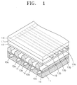
- FIG. 1 An example of an AC type plasma display panel is shown in FIG. 1.
- first electrodes 13a are formed in stripes on the inner side of a rear substrate 11, and a first dielectric layer 14 is formed to cover the first electrodes 13a on the upper surface of the rear substrate 11 where the first electrodes 13a are formed.
- barrier ribs 15 On the upper surface of the first dielectric layer 14 between the first electrodes 13a are formed barrier ribs 15 that keep a discharge distance and that prevent cross talk between discharge cells 19 from occurring.
- a front substrate 12 is joined to the rear substrate 11 where the barrier ribs are formed, and second electrodes 13b of a stripe type that are perpendicular to the first electrodes 13a are formed on the facing side.
- a second dielectric layer 17 formed to cover the second electrodes 12b.
- the dielectric layers 14 and 17 are formed in order to obtain a high discharge strength and memory effect by repeatedly generating avalanche discharge phenomena of wall charges on the surfaces of the dielectric layers.
- a protection layer 18 which protects the dielectric layer 17 from damage by the sputtering of plasma particles and plays the role of lowering a discharge voltage and a maintenance voltage by secondary electron emission.
- a MgO thin film by deposition is generally used for the protection layer.
- a fluorescent layer 16 is formed on the surface of the barrier ribs 15 inside of the discharge cells 19 that are partitioned by the barrier ribs 15 and on the upper surface of the first dielectric layer 14, and an inert gas such as argon is filled inside of the discharge cells.
- ultra-violet rays generated by the voltage applied between the electrodes 13a and 13b excite the fluorescent layer 16 that is formed inside of the discharge cells, and the fluorescent layer 16 emits visible light according to the principle of photoluminescence.
- colors are displayed by red(R), green(G), and blue(B) fluorescent materials that are formed inside of the discharge cells.
- the second dielectric layer 17 is used to obtain a high discharge strength and memory effect, and a second dielectric layer based on PbO has been used in general.
- pinholes are easily formed on the surface of this dielectric layer, thus lowering the insulation characteristics. As a result, the production rate of defective panels in manufacturing plasma display panels becomes high.
- the plasma display panel comprises: a rear substrate; a plurality of first electrodes formed on the inner side of the rear substrate; a first dielectric layer formed over the first electrodes and the rear substrate exposed between the first electrodes; barrier ribs with a predetermined height formed between the first electrodes on the first dielectric layer; a fluorescent layer formed on the side of the barrier ribs and on the dielectric layer between the barrier ribs; a front substrate that is joined to the rear substrate, thus forming discharge spaces partitioned by the barrier ribs; a plurality of second electrodes formed corresponding to the first electrodes on the inner side of the front substrate; and a second dielectric layer formed on the second electrodes and on the inner side of the front substrate exposed between the second electrodes that is composed of a dielectric material whose energy band gap is more than 6 eV and whose dielectric constant is less than 10.
- the present invention may provide a plasma display panel having a second dielectric layer whose light transmittance through the front substrate is excellent and whose interface characteristics are good and having improved image quality due to homogeneous discharge.
- a protection layer is preferably formed on the lower surface of the second dielectric layer, the second dielectric layer is formed to a thickness of more than 5 ⁇ m, and the protection layer is preferably formed to a thickness of more than 500 nm.
- breakdown of the dielectric layer can be reduced by forming on the front substrate a dielectric layer with a high breakdown voltage and good interface characteristics, and as a result, the cost of manufacturing a large quantity of plasma display panels can be reduced by improving the yield of non-defective panels, and the lifetime of the panel can be extended.
- FIG. 2 shows a preferred embodiment of a plasma display panel according to the present invention where the second dielectric layer formed on the front substrate is composed of a CaF 2 thin film.
- a plurality of first and second electrodes 23a and 23b are formed with a stripe pattern on the inner side of each of front and rear substrates 21 and 22.
- a first dielectric layer 24 is formed on the upper surface of the rear substrate 21 to cover the first electrodes 23a, and barrier ribs 25 are formed between the first electrodes 23a on the upper side of the first dielectric layer 24. Also, a fluorescent layer 26 is formed on the sides of the barrier ribs 25 and on the upper surface of the first dielectric layer 24.
- the electrodes 23a and 23b, the first dielectric layer 24, the barrier ribs 25 and the fluorescent layer 26 have the same functions as those in the conventional plasma display panel mentioned earlier.
- the second dielectric layer 27 that is composed of a CaF 2 thin film, and a MgO protection layer 28 are consecutively formed on the inner side of the front substrate 22.
- the material of the second dielectric layer 27 formed on the front substrate 22 (CaF 2 ) is different from that of the prior art and its thickness is more than 5 ⁇ m.
- This CaF 2 thin film has a large thermal expansion coefficient (26 ⁇ 10 -6 cm/K), its light transmittance is excellent (the permissible thickness of light transmittance is 0.2-12 ⁇ m) and its interface characteristics are excellent.
- the MgO protection layer 28 deposited by sputtering or electron beam deposition to a thickness of more than 500 ⁇ m.
- the surface and the cross section on which CaF 2 is deposited by electron beam deposition under the condition of FIG. 3 are examined and its insulation characteristics are also investigated.
- a Ag electrode 51 is printed on the upper surface of a glass substrate 50, a CaF 2 thin film 52 is deposited over the resulting structure and a Cr electrode 53 is formed on the CaF 2 thin film 52 above the Ag electrode 51..
- the insulation characteristics are determined by measuring a breakdown voltage and its surface characteristics are compared with those of a transparent dielectric made of the conventional dielectric layer. By examining the pin hole, etc. found in the conventional dielectric body using this surface inspection, the lifetime and the homogeneity of images of the plasma display panel due to such pin hole, etc. can be anticipated. For its cross sectional characteristics, the distribution of thicknesses is measured.
- the result of measuring breakdown voltage after depositing CaF 2 showed that the breakdown voltage was three times higher than that of the conventional dielectric (30 V/ ⁇ m or so).
- the pin hole, etc. where the voltage drop occurs rapidly are easily formed and an electron field is concentrated in the pin hole, etc., thus lowering the insulation characteristics, but in the case of CaF 2 deposition, the pin hole, etc. did not appear, thus reducing non-defective panels and extending the lifetime of the plasma display panel.
- the transmittance depends on the thickness, but the transmittance did not affect the performance of the plasma display panel even at thicknesses of 5 ⁇ m through 10 ⁇ m, which is thick enough to overcome the breakdown.
- a CaF 2 thin film is representatively explained as the second dielectric layer formed on the front substrate, but as in the case of the CaF 2 dielectric layer, other thin films whose substrate component is a material with a large energy band gap (E g : energy band gap > 6eV) and a low dielectric constant ( ⁇ : dielectric constant ⁇ 10) show effects similar to the CaF 2 thin film.
- Such materials include oxides such as Al 2 O 3 and ZnO and fluorides such as LiF, BaF 2 , SrF, MgF 2 .
- the breakdown voltage of the dielectric layer with excellent light transmittance and interface characteristics which is formed on the front substrate of the plasma display panel according to the present invention is higher than that of the prior art, and the pin hole, etc. are not formed on the surface, thus extending the lifetime of the plasma display panel and guaranteeing a homogeneous thin film protection layer.
Landscapes
- Physics & Mathematics (AREA)
- Engineering & Computer Science (AREA)
- Plasma & Fusion (AREA)
- Gas-Filled Discharge Tubes (AREA)
Abstract
Description
Claims (6)
- A plasma display panel comprising:a rear substrate;a plurality of first electrodes formed on the inner side of the rear substrate;a first dielectric layer that is formed over the first electrodes and exposed portions of the rear substrate between the first electrodes;barrier ribs with a predetermined height formed between the first electrodes on the first dielectric layer;a fluorescent layer that is formed on the side of the barrier ribs and on the dielectric layer between the barrier ribs;a front substrate that is joined to the rear substrate, thus forming discharge spaces partitioned by the barrier ribs;a plurality of second electrodes formed corresponding to the first electrodes on the inner side of the front substrate; anda second dielectric layer formed over the second electrodes and exposed portions of the front substrate between the second electrodes and composed of a dielectric material whose energy band gap is more than 6 eV and whose dielectric constant is less than 10.
- The plasma display panel of claim 1, whereinthe second dielectric layer is composed of one material selected from the group consisting of CaF2, LiF, BaF2, SrF, MgF2, Al2O3 and ZnO
- The plasma display panel of claim 1 or 2, whereinthe thickness of the second dielectric layer is more than 5 µm.
- The plasma display panel of any preceding claim further comprisinga protection layer that is formed on the lower surface of the second dielectric layer.
- The plasma display panel of claim 4, whereinthe protection layer is formed with MgO.
- The plasma display panel of claim 4 or 5, whereinthe thickness of the protection layer is more than 500 µm.
Applications Claiming Priority (2)
| Application Number | Priority Date | Filing Date | Title |
|---|---|---|---|
| KR1020000064216A KR20020033951A (en) | 2000-10-31 | 2000-10-31 | Plasma display panel |
| KR2000064216 | 2000-10-31 |
Publications (2)
| Publication Number | Publication Date |
|---|---|
| EP1202318A2 true EP1202318A2 (en) | 2002-05-02 |
| EP1202318A3 EP1202318A3 (en) | 2002-07-17 |
Family
ID=19696325
Family Applications (1)
| Application Number | Title | Priority Date | Filing Date |
|---|---|---|---|
| EP01301641A Withdrawn EP1202318A3 (en) | 2000-10-31 | 2001-02-23 | Plasma display panel |
Country Status (4)
| Country | Link |
|---|---|
| US (1) | US20020050791A1 (en) |
| EP (1) | EP1202318A3 (en) |
| JP (1) | JP2002150946A (en) |
| KR (1) | KR20020033951A (en) |
Families Citing this family (1)
| Publication number | Priority date | Publication date | Assignee | Title |
|---|---|---|---|---|
| KR100761254B1 (en) * | 2001-03-07 | 2007-09-28 | 엘지전자 주식회사 | Top plate structure of plasma display panel device and its manufacturing method |
Family Cites Families (9)
| Publication number | Priority date | Publication date | Assignee | Title |
|---|---|---|---|---|
| US4048533A (en) * | 1971-10-12 | 1977-09-13 | Owens-Illinois, Inc. | Phosphor overcoat |
| JPS5263663A (en) * | 1975-11-19 | 1977-05-26 | Fujitsu Ltd | Gas electric discharge panel |
| JPS53112056A (en) * | 1977-03-11 | 1978-09-30 | Fujitsu Ltd | Gas discharging panel of self shift type |
| JPS6023457B2 (en) * | 1980-02-29 | 1985-06-07 | 富士通株式会社 | Method for manufacturing electrodes for display panels |
| JP3163563B2 (en) * | 1995-08-25 | 2001-05-08 | 富士通株式会社 | Surface discharge type plasma display panel and manufacturing method thereof |
| US5980347A (en) * | 1996-07-25 | 1999-11-09 | Jsr Corporation | Process for manufacturing plasma display panel |
| JP3119240B2 (en) * | 1998-06-24 | 2000-12-18 | 日本電気株式会社 | Plasma display panel and method of manufacturing the same |
| JP3428446B2 (en) * | 1998-07-09 | 2003-07-22 | 富士通株式会社 | Plasma display panel and method of manufacturing the same |
| EP1119015A4 (en) * | 1998-09-29 | 2007-08-22 | Hitachi Hppl | METHOD FOR MANUFACTURING A PLASMA SCREEN AND SUBSTRATE STRUCTURE |
-
2000
- 2000-10-31 KR KR1020000064216A patent/KR20020033951A/en not_active Ceased
-
2001
- 2001-02-23 EP EP01301641A patent/EP1202318A3/en not_active Withdrawn
- 2001-02-28 US US09/794,095 patent/US20020050791A1/en not_active Abandoned
- 2001-08-31 JP JP2001263860A patent/JP2002150946A/en active Pending
Also Published As
| Publication number | Publication date |
|---|---|
| KR20020033951A (en) | 2002-05-08 |
| JP2002150946A (en) | 2002-05-24 |
| EP1202318A3 (en) | 2002-07-17 |
| US20020050791A1 (en) | 2002-05-02 |
Similar Documents
| Publication | Publication Date | Title |
|---|---|---|
| US6657396B2 (en) | Alternating current driven type plasma display device and method for production thereof | |
| JP4532718B2 (en) | Secondary electron amplification structure using carbon nanotube, plasma display panel and backlight using the same | |
| US6965200B2 (en) | Plasma display device having barrier ribs | |
| JP4479144B2 (en) | Plasma display device and manufacturing method thereof | |
| US6960882B2 (en) | Plasma display device and manufacturing method thereof | |
| US7408300B2 (en) | Alternating current driven type plasma display device and production method therefor | |
| US20020050791A1 (en) | Plasma display panel | |
| US7969093B2 (en) | Plasma display panel with contrast-improving composition in the barrier layer | |
| JP4532329B2 (en) | Plasma display panel | |
| EP2083437A1 (en) | Plasma display panel having high clarity and color purity | |
| US20080238312A1 (en) | Plasma display panel | |
| KR100637230B1 (en) | Plasma display panel | |
| KR100468831B1 (en) | Plasma display panel and method of manufacturing the same | |
| US7420328B2 (en) | Plasma display panel design that compensates for differing surface potential of colored fluorescent material | |
| JP2003197110A (en) | Plasma display panel | |
| KR100708709B1 (en) | Plasma display panel | |
| JP2003132799A (en) | AC driven plasma display | |
| US7187127B2 (en) | Plasma display panel having exothermal inhibition layer | |
| US7271539B2 (en) | Plasma display panel | |
| US7768205B2 (en) | Plasma display panel and method of manufacturing the same | |
| KR20000001613A (en) | Plasma display panel | |
| KR20060133283A (en) | Plasma display panel | |
| KR100562861B1 (en) | Plasma display panel | |
| KR100922751B1 (en) | Plasma display panel | |
| US20070029934A1 (en) | Plasma display panel |
Legal Events
| Date | Code | Title | Description |
|---|---|---|---|
| PUAI | Public reference made under article 153(3) epc to a published international application that has entered the european phase |
Free format text: ORIGINAL CODE: 0009012 |
|
| AK | Designated contracting states |
Kind code of ref document: A2 Designated state(s): AT BE CH CY DE DK ES FI FR GB GR IE IT LI LU MC NL PT SE TR |
|
| AX | Request for extension of the european patent |
Free format text: AL;LT;LV;MK;RO;SI |
|
| PUAL | Search report despatched |
Free format text: ORIGINAL CODE: 0009013 |
|
| AK | Designated contracting states |
Kind code of ref document: A3 Designated state(s): AT BE CH CY DE DK ES FI FR GB GR IE IT LI LU MC NL PT SE TR |
|
| AX | Request for extension of the european patent |
Free format text: AL;LT;LV;MK;RO;SI |
|
| 17P | Request for examination filed |
Effective date: 20021030 |
|
| AKX | Designation fees paid |
Designated state(s): DE FR GB |
|
| STAA | Information on the status of an ep patent application or granted ep patent |
Free format text: STATUS: THE APPLICATION IS DEEMED TO BE WITHDRAWN |
|
| 18D | Application deemed to be withdrawn |
Effective date: 20060901 |