EP1202067A2 - Phase detector - Google Patents
Phase detector Download PDFInfo
- Publication number
- EP1202067A2 EP1202067A2 EP01308984A EP01308984A EP1202067A2 EP 1202067 A2 EP1202067 A2 EP 1202067A2 EP 01308984 A EP01308984 A EP 01308984A EP 01308984 A EP01308984 A EP 01308984A EP 1202067 A2 EP1202067 A2 EP 1202067A2
- Authority
- EP
- European Patent Office
- Prior art keywords
- input
- output
- phase
- xor gate
- xor
- Prior art date
- Legal status (The legal status is an assumption and is not a legal conclusion. Google has not performed a legal analysis and makes no representation as to the accuracy of the status listed.)
- Withdrawn
Links
- 238000001514 detection method Methods 0.000 claims abstract description 10
- 238000000034 method Methods 0.000 claims description 12
- 238000001914 filtration Methods 0.000 claims description 10
- 230000003111 delayed effect Effects 0.000 claims description 6
- 230000001934 delay Effects 0.000 claims description 3
- 230000002238 attenuated effect Effects 0.000 abstract description 4
- 239000003990 capacitor Substances 0.000 description 3
- 238000010586 diagram Methods 0.000 description 2
- 230000000694 effects Effects 0.000 description 2
- 238000012935 Averaging Methods 0.000 description 1
- 230000000295 complement effect Effects 0.000 description 1
- 238000012986 modification Methods 0.000 description 1
- 230000004048 modification Effects 0.000 description 1
- 238000010587 phase diagram Methods 0.000 description 1
Images


Classifications
-
- H—ELECTRICITY
- H03—ELECTRONIC CIRCUITRY
- H03D—DEMODULATION OR TRANSFERENCE OF MODULATION FROM ONE CARRIER TO ANOTHER
- H03D13/00—Circuits for comparing the phase or frequency of two mutually-independent oscillations
-
- H—ELECTRICITY
- H03—ELECTRONIC CIRCUITRY
- H03D—DEMODULATION OR TRANSFERENCE OF MODULATION FROM ONE CARRIER TO ANOTHER
- H03D13/00—Circuits for comparing the phase or frequency of two mutually-independent oscillations
- H03D13/003—Circuits for comparing the phase or frequency of two mutually-independent oscillations in which both oscillations are converted by logic means into pulses which are applied to filtering or integrating means
-
- H—ELECTRICITY
- H03—ELECTRONIC CIRCUITRY
- H03L—AUTOMATIC CONTROL, STARTING, SYNCHRONISATION OR STABILISATION OF GENERATORS OF ELECTRONIC OSCILLATIONS OR PULSES
- H03L7/00—Automatic control of frequency or phase; Synchronisation
- H03L7/06—Automatic control of frequency or phase; Synchronisation using a reference signal applied to a frequency- or phase-locked loop
- H03L7/08—Details of the phase-locked loop
- H03L7/085—Details of the phase-locked loop concerning mainly the frequency- or phase-detection arrangement including the filtering or amplification of its output signal
Definitions
- the field of the invention is phase detection especially in digital circuitry, and more specifically high precision input characteristic phase detection circuitry.
- analog circuits have been utilized to detect the phase of two inputs.
- analog mixers have been used for phase detection.
- analog mixers are more expensive and less convenient than digital circuits. In some applications, analog mixers are simply impractical.
- XOR exclusive-OR
- the resulting output of the XOR gate is known to be a low level output (i.e. , zero volts).
- the two inputs are one-hundred eighty degrees out of phase, the resulting output of the XOR gate is known to be a high level output.
- the transducer gain and offset of these results are sensitive to variations of temperature and supply voltage. Consequently, the precision and accuracy of a XOR gate phase detector is lacking.
- the present invention is an apparatus and method for detecting phase with precision.
- the present invention utilizes a pair of logic gates applied to two inputs to allow the inputs to be processed by a differential amplifier to determine the phase of the inputs.
- the pair of logic gates are preferably XOR gates that perform exclusive OR operations on the two inputs.
- the first XOR gate performs an exclusive OR operation on a first input and a second input.
- the second XOR gate performs an exclusive OR operation on the first input and the inverted second input.
- the outputs of the second XOR gate and the first XOR gate are then subtracted to remove any common errors, such as those caused by temperature and input voltage variation.
- the result of the subtraction is a phase indicating voltage that is without these common errors. From known voltage levels of the phase indicating voltage, the phase of the first input and the second input can be determined. The phase indicating voltage is at a minimum level when the first input and the second input are zero degrees out of phase ( i.e. , in phase), a medium level when the first input and the second input are ninety degrees out of phase and a maximum level when the first input and the second input are one-hundred eighty degrees out of phase. Accordingly, the phase detection is accomplished with high precision and accuracy.
- An embodiment of the present invention utilizes two additional XOR gates.
- the third XOR gate is used to insert a propagation delay into the second input. This propagation delay is inserted to match the propagation delay caused by the fourth XOR gate which is used to invert the second input.
- the outputs of the third XOR gate and the fourth XOR gate are transmitted to the first XOR gate and the second XOR gate, respectively, for the exclusive OR operations with the first input.
- Use of four XOR gates is particularly convenient since XOR gates are often sold in packages of four gates.
- the desired output of a phase detector is a low frequency average voltage resulting from lowpass filtering of the XOR gate output waveforms.
- This filtering may be inserted after each gate before a differential amplifier which may perform the subtracting of the waveforms or the differential amplifier may provide some or all of this filtering, either by its own characteristics or by appropriate feedback components, or the differential amplifier may be followed by a lowpass filter.
- two capacitors are associated with the differential amplifier for this purpose.
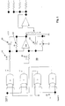
- Figure 1 is a block diagram of circuitry of an embodiment of the present invention.
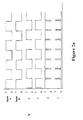
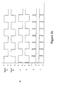
- FIGS 2a-2c illustrate sample input wave forms and the function of circuitry of an embodiment of the present invention.
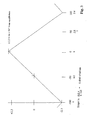
- Figure 3 is a diagram of a phase indicating voltage of an embodiment of the present invention over a range of phases.
- Figure 4 is a flowchart of a method of the present invention.
- Figure 1 illustrates an exemplary embodiment of the Phase Detector with High Precision 10 of the present invention.
- the embodiment shown utilizes exclusive OR ("XOR") logic gates in combination with a differential amplifier to precisely determine the phase difference, as an analog signal, of two measured digital waveform inputs. Since logic gates are used, the input signals need to be logic level signals as opposed to analog signals. If the inputs are analog signals, hard limiters would need to be applied to the analog signals.
- XOR exclusive OR
- the two input signals in this embodiment are Input A and Input B.
- Input A and B are both 5 volt square waves with a fifty-percent (50%) duty cycle.
- the input signals are largely determined by the application in which the present invention is used. Accordingly, a variety of voltages, waveforms and duty-cycles may be used.
- Figures 2a-2c illustrate various Input A and B signals.
- Inputs A and B are applied to four XOR logic gates.
- the four XOR logic gates are labeled 1-4.
- XOR gates 1 and 2 compare Input A and Input B as modified by XOR gates 3 and 4.
- XOR gate 4 performs an exclusive OR operation on Input B and a constant high-level input 20.
- the constant high-level input 20 voltage is preferably equal to the high-level voltage of Input B. Accordingly, in the present embodiment, the constant high-level input 20 is 5 volts.
- the output of XOR gate 4 is low ( i.e. , 0 volts), after an inherent propagation delay, when Input B is high ( i.e. , 5 volts).
- XOR gate 4 is high (i.e. , 5 volts), after the inherent delay, when Input B is low (i.e. , 0 volts). In other words, XOR gate 4 inverts and delays Input B. Referring to Figures 2a-2c, the output of XOR gate 4 is seen with the inherent delay effect. The output of XOR gate 4 is input to XOR gate 2.
- XOR gate 3 Since the output of XOR gate 4 includes an inherent delay, Input B must also be delayed before being input into XOR gate 1. Accordingly, XOR gate 3 performs an exclusive OR operation on Input B and a ground input 25. The output of XOR gate 3 is Input B with an inherent propagation delay that preferably matches the inherent propagation delay caused by XOR gate 4, as seen in Figures 2a-2c. The output of XOR gate 3 is input to XOR gate 1.
- XOR gate 1 performs an exclusive OR operation on Input A and the output of XOR gate 3 (i.e. , Input B with the inherent delay from XOR gate 3). Accordingly, the output of XOR gate 1 is low, with an inherent delay, when Input A and the output of XOR gate 3 are both high (e.g., 5 volts) or both low ( e.g. , 0 volts). As such, if the phases of Input A and Input B are the same ( i.e. , zero degrees (0°) out of phase), then the output of XOR gate 1 will be constantly low, except for a brief pulse due to the delay caused by XOR gate 3. Such a situation is illustrated in Figure 2a. In Figure 2a, Input A and Input B are zero degrees out of phase, and therefore, the output of XOR gate 1 is low, except for the aforementioned pulse.
- a minimum output is seen at a phase angle of one-hundred eighty degrees (i.e. , when Input A and Input B are 180°out of phase)
- a middle output is seen at a phase angle of ninety degrees (i.e. , when Input A and Input B are 90° out of phase)
- a maximum output is seen at a phase angle of zero degrees (i.e. , when Input A and Input B are 0° out of phase).
- a phase lock loop would track as shown in Figure 3 if the phase detector 10 were used as the phase detector in the phase lock loop.
- XOR gate 1 with inputs from Input A and Input B, may be used by itself as a phase detector.
- a logic gate such as XOR gate 1
- the DC level of the output of the logic gate will be subject to variations, particularly due to temperature and to some extent due to the supply voltage on the logic gate.
- One way to minimize these errors is to provide a second section with an output of the complementary function to XOR gate 1 and to subtract the outputs of XOR gate 1 and the second section.
- a differential amplifier may be used to combine and subtract these outputs. So subtracted, common variations, such as from temperature or supply voltage changes, will tend to be subtracted or canceled out by the differential amplifier. Consequently, the phase detector will have improved stability, with regards to temperature and supply voltage, in comparison to the single logic gate phase detector.
- XOR gate 2 performs an exclusive OR on Input A and the output of XOR gate 4 (i.e. , inverted Input B with an inherent delay caused by XOR gate 4). Accordingly, the output of XOR gate 2 is low, with an inherent delay, when Input A and the output of XOR gate 4 are both high (e.g., 5 volts) or both low (e.g., 0 volts). As such, if the phases of Input A and Input B are the same (i.e.
- the outputs of XOR gate 1 and XOR gate 2 are combined and subtracted by a differential amplifier 440.
- the differential amplifier 440 will subtract out errors common to both XOR gate 1 and XOR gate 2.
- the output of XOR gate 2 is input into the positive input ("+") of the differential amplifier 440 and the output of XOR gate 1 is input into the negative input (“-”) of the differential amplifier 440. Consequently, errors common to both outputs will be treated oppositely by the differential amplifier 440 ( i.e. , they will be positive for one input and negative for the other input) and will therefore cancel out.
- the differential amplifier 440 and its surrounding components may be designed to attenuate, filter and, as stated above, subtract the XOR gate 1 and XOR gate 2 outputs.
- the outputs may be attenuated to provide a voltage level appropriate for the application in which the phase detector is used.
- Low-pass filtering of the XOR gate outputs may be utilized to achieve a desired low frequency average voltage for the phase detector output. This low-pass filtering may be inserted after each gate before the amplifier 440, the amplifier 440 may provide some or all of this filtering, either by its own characteristics or by appropriate feedback and other components, or the amplifier 440 may be followed by a low-pass filter. If a different frequency average voltage for the phase detector output is desired, different filtering may be utilized.
- the outputs of XOR gate 1 and XOR gate 2 are both attenuated by input resistors 50 and resistors 55.
- the input resistors 50 are 2.15 kO resistors and the resistors 55 are 1.0 kO resistors. Consequently, the outputs of XOR gate 1 and XOR gate 2 are attenuated by a factor of 2.15 ( i.e. , 2.15 kO/1.00 kO).
- the attenuation of 2.15 produces an output range for the differential amplifier 440 of approximately -2.32 volts to 2.32 volts.
- the outputs of XOR gate 1 and XOR gate 2 are low-pass filtered by the differential amplifier 440 and the surrounding components in the present embodiment.
- the capacitors 60 in cooperation with the resistors 55, function as low pass filters that cause the low-frequency averages of the pulse waveform outputs from XOR gate 1 and XOR gate 2 to be combined differentially in the differential amplifier 440.
- the low-pass filtering of the XOR gate 1 and XOR gate 2 outputs produces a constant phase indicating voltage P1 at each phase, averaging out the brief pulses shown in Figures 2a and 2c.
- the resultant output P1 of the differential amplifier 440 is illustrated by Figure 3.
- the minimum output, ⁇ -2.32 volts is a result of the combined low frequency average of the nearly constant high output of XOR gate 1 and the nearly constant low, or zero, output of XOR gate 2, as discussed above and as seen in Figure 2c.
- Input A and Input B are ninety degrees (90°) out of phase, the output P1 is at a medium level.
- the medium output, 0 volts, is a result of the combined low frequency average of the outputs of XOR gate 1 and XOR gate 2 that are constantly oppositely high and low, as discussed above and as seen in Figure 2b.
- the output P1 is at a maximum.
- the maximum output, ⁇ 2.32 volts is a result of the combined low frequency average of the nearly constant high output of XOR gate 2 and the nearly constant low, or zero, output of XOR gate 1, as discussed above and as seen in Figure 2a.
- the phase indicating voltage in the present embodiment i.e. , output P1
- the phase of Input A and Input B can be determined from the output voltage of output P1.
- the rate of change in output P 1 per radian change in the phase of Input A and Input B can also be determined by calculating the slope of P 1 in Figure 3.
- a phase detection method 40 is illustrated in Figure 4.
- the method 40 comprises performing an XOR operation on a first input and a second input to produce a first output 41, inverting the second input 42, performing an XOR operation on the first input and the inverted second input to produce a second output 43, subtracting the second output from the first output to produce a phase indicating voltage 44 and measuring the phase indicating voltage to determine the phase of the first input and the second input 45, wherein the phase indicating voltage is at a maximum when the first input and the second input are zero degrees out of phase and at a minimum when the first input and the second input are one-hundred eighty degrees out of phase.
- the method may also include delaying the second input and the inverted second input (not shown in Figure 4), attenuating the first output and the second output (not shown in Figure 4) and low-pass filtering the first output and the second output (not shown in Figure 4), as well as other steps that are apparent from the above description and Figures.
- phase Detector and the method of phase detection described above may be used in a variety of applications requiring phase detection.
- the additional circuitry shown in Figure 3 is for a particular implementation and is not required by the present invention.
- the variable resistor shown following the differential amplifier 440 may be used to adjust the slope or transducer gain of this phase detection process.
Landscapes
- Engineering & Computer Science (AREA)
- Power Engineering (AREA)
- Manipulation Of Pulses (AREA)
- Stabilization Of Oscillater, Synchronisation, Frequency Synthesizers (AREA)
- Digital Transmission Methods That Use Modulated Carrier Waves (AREA)
Abstract
A phase detector (10) detects the phase of two inputs (A, B) with precision by subtracting out common errors due to temperature variations and input voltage fluctuations. The phase detector utilizes digital circuitry comprising exclusive OR gates (1, 2) and a differential amplifier (440) to perform the accurate phase detection. The inputs and outputs may be attenuated or filtered to produce the desired results.
Description
- The field of the invention is phase detection especially in digital circuitry, and more specifically high precision input characteristic phase detection circuitry.
- Detecting the phase of two inputs has presented unique challenges. In the past, analog circuits have been utilized to detect the phase of two inputs. Specifically, analog mixers have been used for phase detection. Unfortunately, analog mixers are more expensive and less convenient than digital circuits. In some applications, analog mixers are simply impractical.
- One digital circuit solution has been to use exclusive-OR ("XOR") gates as phase detectors. If the two inputs are in phase, the resulting output of the XOR gate is known to be a low level output (i.e., zero volts). Likewise, if the two inputs are one-hundred eighty degrees out of phase, the resulting output of the XOR gate is known to be a high level output. Unfortunately, the transducer gain and offset of these results are sensitive to variations of temperature and supply voltage. Consequently, the precision and accuracy of a XOR gate phase detector is lacking.
- What is needed is a digital circuit phase detector that is precise and accurate and is not substantially susceptible to errors such as those caused by temperature or supply voltage variations.
- The present invention is an apparatus and method for detecting phase with precision. In an embodiment, the present invention utilizes a pair of logic gates applied to two inputs to allow the inputs to be processed by a differential amplifier to determine the phase of the inputs. The pair of logic gates are preferably XOR gates that perform exclusive OR operations on the two inputs. The first XOR gate performs an exclusive OR operation on a first input and a second input. The second XOR gate performs an exclusive OR operation on the first input and the inverted second input. The outputs of the second XOR gate and the first XOR gate are then subtracted to remove any common errors, such as those caused by temperature and input voltage variation.
- The result of the subtraction is a phase indicating voltage that is without these common errors. From known voltage levels of the phase indicating voltage, the phase of the first input and the second input can be determined. The phase indicating voltage is at a minimum level when the first input and the second input are zero degrees out of phase (i.e., in phase), a medium level when the first input and the second input are ninety degrees out of phase and a maximum level when the first input and the second input are one-hundred eighty degrees out of phase. Accordingly, the phase detection is accomplished with high precision and accuracy.
- An embodiment of the present invention utilizes two additional XOR gates. The third XOR gate is used to insert a propagation delay into the second input. This propagation delay is inserted to match the propagation delay caused by the fourth XOR gate which is used to invert the second input. The outputs of the third XOR gate and the fourth XOR gate are transmitted to the first XOR gate and the second XOR gate, respectively, for the exclusive OR operations with the first input. Use of four XOR gates is particularly convenient since XOR gates are often sold in packages of four gates.
- In a preferred embodiment, the desired output of a phase detector is a low frequency average voltage resulting from lowpass filtering of the XOR gate output waveforms. This filtering may be inserted after each gate before a differential amplifier which may perform the subtracting of the waveforms or the differential amplifier may provide some or all of this filtering, either by its own characteristics or by appropriate feedback components, or the differential amplifier may be followed by a lowpass filter. In the embodiment shown, two capacitors are associated with the differential amplifier for this purpose.
- Figure 1 is a block diagram of circuitry of an embodiment of the present invention.
- Figures 2a-2c illustrate sample input wave forms and the function of circuitry of an embodiment of the present invention.
- Figure 3 is a diagram of a phase indicating voltage of an embodiment of the present invention over a range of phases.
- Figure 4 is a flowchart of a method of the present invention.
- Figure 1 illustrates an exemplary embodiment of the Phase Detector with
High Precision 10 of the present invention. The embodiment shown utilizes exclusive OR ("XOR") logic gates in combination with a differential amplifier to precisely determine the phase difference, as an analog signal, of two measured digital waveform inputs. Since logic gates are used, the input signals need to be logic level signals as opposed to analog signals. If the inputs are analog signals, hard limiters would need to be applied to the analog signals. - The two input signals in this embodiment are Input A and Input B. In the example shown, Input A and B are both 5 volt square waves with a fifty-percent (50%) duty cycle. The input signals are largely determined by the application in which the present invention is used. Accordingly, a variety of voltages, waveforms and duty-cycles may be used. Figures 2a-2c illustrate various Input A and B signals.
- As shown in Figure 1, Inputs A and B are applied to four XOR logic gates. The four XOR logic gates are labeled 1-4.
XOR gates XOR gates gate 4 performs an exclusive OR operation on Input B and a constant high-level input 20. The constant high-level input 20 voltage is preferably equal to the high-level voltage of Input B. Accordingly, in the present embodiment, the constant high-level input 20 is 5 volts. As a result, the output ofXOR gate 4 is low (i.e., 0 volts), after an inherent propagation delay, when Input B is high (i.e., 5 volts). Likewise, the output ofXOR gate 4 is high (i.e., 5 volts), after the inherent delay, when Input B is low (i.e., 0 volts). In other words,XOR gate 4 inverts and delays Input B. Referring to Figures 2a-2c, the output ofXOR gate 4 is seen with the inherent delay effect. The output ofXOR gate 4 is input toXOR gate 2. - Since the output of
XOR gate 4 includes an inherent delay, Input B must also be delayed before being input intoXOR gate 1. Accordingly, XORgate 3 performs an exclusive OR operation on Input B and a ground input 25. The output ofXOR gate 3 is Input B with an inherent propagation delay that preferably matches the inherent propagation delay caused byXOR gate 4, as seen in Figures 2a-2c. The output ofXOR gate 3 is input toXOR gate 1. -
XOR gate 1 performs an exclusive OR operation on Input A and the output of XOR gate 3 (i.e., Input B with the inherent delay from XOR gate 3). Accordingly, the output ofXOR gate 1 is low, with an inherent delay, when Input A and the output ofXOR gate 3 are both high (e.g., 5 volts) or both low (e.g., 0 volts). As such, if the phases of Input A and Input B are the same (i.e., zero degrees (0°) out of phase), then the output ofXOR gate 1 will be constantly low, except for a brief pulse due to the delay caused byXOR gate 3. Such a situation is illustrated in Figure 2a. In Figure 2a, Input A and Input B are zero degrees out of phase, and therefore, the output ofXOR gate 1 is low, except for the aforementioned pulse. - Oppositely, if Input A and Input B are one-hundred eighty degrees (180°) out of phase, then the output of
XOR gate 1 will be constantly high, except for a brief pulse due to the delay caused byXOR gate 3. Figure 2c illustrates this situation and result. On the other hand, when Input A and Input B are ninety degrees (90°) out of phase, the output ofXOR gate 1 will be alternatively high and low, with a smaller duty cycle and narrower wave form then Input A and Input B. Figure 2b illustrates this situation and result. - Referring to Figure 3, we see that the above results correspond with the phase diagram shown. A minimum output is seen at a phase angle of one-hundred eighty degrees (i.e., when Input A and Input B are 180°out of phase), a middle output is seen at a phase angle of ninety degrees (i.e., when Input A and Input B are 90° out of phase) and a maximum output is seen at a phase angle of zero degrees (i.e., when Input A and Input B are 0° out of phase). A phase lock loop would track as shown in Figure 3 if the
phase detector 10 were used as the phase detector in the phase lock loop. -
XOR gate 1, with inputs from Input A and Input B, may be used by itself as a phase detector. However, if a logic gate such asXOR gate 1 is used as a phase detector, the DC level of the output of the logic gate will be subject to variations, particularly due to temperature and to some extent due to the supply voltage on the logic gate. One way to minimize these errors is to provide a second section with an output of the complementary function toXOR gate 1 and to subtract the outputs ofXOR gate 1 and the second section. A differential amplifier may be used to combine and subtract these outputs. So subtracted, common variations, such as from temperature or supply voltage changes, will tend to be subtracted or canceled out by the differential amplifier. Consequently, the phase detector will have improved stability, with regards to temperature and supply voltage, in comparison to the single logic gate phase detector. - It follows then that
XOR gate 2 performs an exclusive OR on Input A and the output of XOR gate 4 (i.e., inverted Input B with an inherent delay caused by XOR gate 4). Accordingly, the output ofXOR gate 2 is low, with an inherent delay, when Input A and the output ofXOR gate 4 are both high (e.g., 5 volts) or both low (e.g., 0 volts). As such, if the phases of Input A and Input B are the same (i.e., zero degrees (0°) out of phase), then the output ofXOR gate 2 will be constantly high (since the output ofXOR gate 4 will be the opposite of Input A, with a delay), except for a brief pulse due to the delay caused byXOR gate 4. Such a situation is illustrated in Figure 2a. In Figure 2a, Input A and Input B are zero degrees out of phase, and therefore, the output ofXOR gate 2 is high, except for the aforementioned pulse. - Oppositely, if Input A and Input B are one-hundred eighty degrees (180°) out of phase, then the output of
XOR gate 2 will be constantly low (since the output ofXOR gate 4 will be the same as Input A, with a delay), except for a brief pulse due to the delay caused byXOR gate 4. Figure 2c illustrates this situation and result. On the other hand, when Input A and Input B are ninety degrees (90°) out of phase, the output ofXOR gate 2 will be alternatively high and low, with a smaller duty cycle and narrower wave form then Input A and Input B. Figure 2b illustrates this situation and result. - As discussed above, the outputs of
XOR gate 1 andXOR gate 2 are combined and subtracted by adifferential amplifier 440. Thedifferential amplifier 440 will subtract out errors common to bothXOR gate 1 andXOR gate 2. As is shown in Figure 1, the output ofXOR gate 2 is input into the positive input ("+") of thedifferential amplifier 440 and the output ofXOR gate 1 is input into the negative input ("-") of thedifferential amplifier 440. Consequently, errors common to both outputs will be treated oppositely by the differential amplifier 440 (i.e., they will be positive for one input and negative for the other input) and will therefore cancel out. For example, an error of .01 volts caused by a voltage supply shift common to bothXOR gate 1 andXOR gate 2 will be treated as -.01 volts in the - input and as .01 volts in the + input, therefore resulting in a net zero volt effect (.01-.01=0) on the output of thedifferential amplifier 440. - The
differential amplifier 440 and its surrounding components (e.g., theinput resistors 50,resistors 55 and capacitors 60) may be designed to attenuate, filter and, as stated above, subtract theXOR gate 1 andXOR gate 2 outputs. The outputs may be attenuated to provide a voltage level appropriate for the application in which the phase detector is used. Low-pass filtering of the XOR gate outputs may be utilized to achieve a desired low frequency average voltage for the phase detector output. This low-pass filtering may be inserted after each gate before theamplifier 440, theamplifier 440 may provide some or all of this filtering, either by its own characteristics or by appropriate feedback and other components, or theamplifier 440 may be followed by a low-pass filter. If a different frequency average voltage for the phase detector output is desired, different filtering may be utilized. - In the present embodiment, the outputs of
XOR gate 1 andXOR gate 2 are both attenuated byinput resistors 50 andresistors 55. In the example shown in Figure 1, theinput resistors 50 are 2.15 kO resistors and theresistors 55 are 1.0 kO resistors. Consequently, the outputs ofXOR gate 1 andXOR gate 2 are attenuated by a factor of 2.15 (i.e., 2.15 kO/1.00 kO). With an input of 5 volts, as in the present example, the attenuation of 2.15 produces an output range for thedifferential amplifier 440 of approximately -2.32 volts to 2.32 volts. - Likewise, the outputs of
XOR gate 1 andXOR gate 2 are low-pass filtered by thedifferential amplifier 440 and the surrounding components in the present embodiment. Thecapacitors 60, in cooperation with theresistors 55, function as low pass filters that cause the low-frequency averages of the pulse waveform outputs fromXOR gate 1 andXOR gate 2 to be combined differentially in thedifferential amplifier 440. As is shown in Figure 3, the low-pass filtering of theXOR gate 1 andXOR gate 2 outputs produces a constant phase indicating voltage P1 at each phase, averaging out the brief pulses shown in Figures 2a and 2c. - The resultant output P1 of the
differential amplifier 440 is illustrated by Figure 3. As discussed above, when Input A and Input B are one-hundred eighty degrees (180°) out of phase, the output P1 is at a minimum. The minimum output, ∼-2.32 volts, is a result of the combined low frequency average of the nearly constant high output ofXOR gate 1 and the nearly constant low, or zero, output ofXOR gate 2, as discussed above and as seen in Figure 2c. Further, when Input A and Input B are ninety degrees (90°) out of phase, the output P1 is at a medium level. The medium output, 0 volts, is a result of the combined low frequency average of the outputs ofXOR gate 1 andXOR gate 2 that are constantly oppositely high and low, as discussed above and as seen in Figure 2b. Finally, when Input A and Input B are zero degrees (0°) out of phase, the output P1 is at a maximum. The maximum output, ∼2.32 volts is a result of the combined low frequency average of the nearly constant high output ofXOR gate 2 and the nearly constant low, or zero, output ofXOR gate 1, as discussed above and as seen in Figure 2a. - As a result, the phase indicating voltage in the present embodiment, i.e., output P1, has a zero-center, bi-polar range that is convenient for many applications. Consequently, with the known range, the phase of Input A and Input B can be determined from the output voltage of output P1. The rate of change in
output P 1 per radian change in the phase of Input A and Input B can also be determined by calculating the slope ofP 1 in Figure 3. In the present example, the slope is approximately 4.64 volts per p radian (p radian = 180°) or approximately 1.464 volts/radian. - A
phase detection method 40 according to the present invention is illustrated in Figure 4. Themethod 40 comprises performing an XOR operation on a first input and a second input to produce afirst output 41, inverting thesecond input 42, performing an XOR operation on the first input and the inverted second input to produce asecond output 43, subtracting the second output from the first output to produce aphase indicating voltage 44 and measuring the phase indicating voltage to determine the phase of the first input and thesecond input 45, wherein the phase indicating voltage is at a maximum when the first input and the second input are zero degrees out of phase and at a minimum when the first input and the second input are one-hundred eighty degrees out of phase. As described above, the method may also include delaying the second input and the inverted second input (not shown in Figure 4), attenuating the first output and the second output (not shown in Figure 4) and low-pass filtering the first output and the second output (not shown in Figure 4), as well as other steps that are apparent from the above description and Figures. - The Phase Detector and the method of phase detection described above may be used in a variety of applications requiring phase detection. The additional circuitry shown in Figure 3 is for a particular implementation and is not required by the present invention. For example, the variable resistor shown following the
differential amplifier 440 may be used to adjust the slope or transducer gain of this phase detection process. While the invention has been described with reference to the exemplary embodiments thereof, those skilled in the art will be able to make various modifications to the described embodiments of the invention without departing from the true spirit and scope of the invention. The terms and descriptions used herein are set forth by way of illustration only and are not meant as limitations. In particular, although the method of the present invention has been described by examples, the steps of the method may be performed in a different order than illustrated or simultaneously. Those skilled in the art will recognize that these and other variations are possible within the scope of the invention as defined in the following claims and their equivalents.
Claims (10)
- A phase detector with high precision (10), comprising:a first input, wherein the first input has a high level and a low level;a second input, wherein the second input has a high level and a low level;a first XOR gate (1) that performs an exclusive OR operation on the first input and the second input to produce a first output;a second XOR gate (2) that performs an exclusive OR operation on the first input and an inverted second input to produce a second output; anda differential amplifier (440) that subtracts the second output from the first output to produce a phase indicating voltage, wherein the phase indicating voltage is at a maximum when the first input and the second input are zero degrees out of phase and the phase indicating voltage is at a minimum when the first input and the second input are one-hundred eighty degrees out of phase.
- The phase detector of claim 1, further comprising:a third XOR gate (3) that delays the second input and transmits the delayed second input to the first XOR gate (1), wherein the first XOR gate (1) performs the exclusive OR operation on the first input and the delayed second input; anda fourth XOR gate (4) that inverts and delays the second input and transmits the delayed, inverted second input to the second XOR gate (2), wherein the second XOR gate (2) performs the exclusive OR operation on the first input and the delayed, inverted second input.
- The phase detector of claim 2, wherein the third XOR gate (3) performs an exclusive OR operation on the second input and a grounded input.
- The phase detector of claim 3, wherein the fourth XOR gate (4) performs an exclusive OR operation on the second input and a high level input that has a voltage equal to the second input high level.
- The phase detector of claim 1, further comprising one or more low-pass filters that filter the first output and the second output so that the differential amplifier (440) subtracts the low-frequency average of the first output and the second output.
- The phase detector of claim 1, further comprising input resistors (50) that attenuate the first output and the second output
- A method of phase detection with high precision, comprising:performing an XOR operation (41) on a first input and a second input to produce a first output;inverting the second input (42);performing an XOR operation (43) on the first input and the inverted second input to produce a second output; andsubtracting the second output from the first output (44) to produce a phase indicating voltage and measuring the phase indicating voltage to determine the phase of the first input and the second input, wherein the phase indicating voltage is at a maximum when the first input and the second input are zero degrees out of phase and at a minimum when the first input and the second input are one-hundred eighty degrees out of phase.
- The method of claim 7, further comprising:delaying the second input and the inverted second input, wherein the second input and the inverted second input are delayed and equivalent period of time.
- The method of claim 7, wherein a differential amplifier performs the subtracting step.
- The method of claim 7, further comprising low-pass filtering the first output and the second output so that the subtracting step comprises subtracting the low-frequency average of the first output and the second output.
Applications Claiming Priority (2)
| Application Number | Priority Date | Filing Date | Title |
|---|---|---|---|
| US698100 | 2000-10-30 | ||
| US09/698,100 US6351153B1 (en) | 2000-10-30 | 2000-10-30 | Phase detector with high precision |
Publications (1)
| Publication Number | Publication Date |
|---|---|
| EP1202067A2 true EP1202067A2 (en) | 2002-05-02 |
Family
ID=24803898
Family Applications (1)
| Application Number | Title | Priority Date | Filing Date |
|---|---|---|---|
| EP01308984A Withdrawn EP1202067A2 (en) | 2000-10-30 | 2001-10-23 | Phase detector |
Country Status (5)
| Country | Link |
|---|---|
| US (1) | US6351153B1 (en) |
| EP (1) | EP1202067A2 (en) |
| JP (1) | JP2002198788A (en) |
| KR (1) | KR20020033537A (en) |
| CN (1) | CN1351415A (en) |
Families Citing this family (14)
| Publication number | Priority date | Publication date | Assignee | Title |
|---|---|---|---|---|
| US7274740B2 (en) * | 2003-06-25 | 2007-09-25 | Sharp Laboratories Of America, Inc. | Wireless video transmission system |
| US9325998B2 (en) | 2003-09-30 | 2016-04-26 | Sharp Laboratories Of America, Inc. | Wireless video transmission system |
| US8018850B2 (en) * | 2004-02-23 | 2011-09-13 | Sharp Laboratories Of America, Inc. | Wireless video transmission system |
| US7784076B2 (en) * | 2004-10-30 | 2010-08-24 | Sharp Laboratories Of America, Inc. | Sender-side bandwidth estimation for video transmission with receiver packet buffer |
| US7797723B2 (en) * | 2004-10-30 | 2010-09-14 | Sharp Laboratories Of America, Inc. | Packet scheduling for video transmission with sender queue control |
| US8356327B2 (en) * | 2004-10-30 | 2013-01-15 | Sharp Laboratories Of America, Inc. | Wireless video transmission system |
| US20070067480A1 (en) * | 2005-09-19 | 2007-03-22 | Sharp Laboratories Of America, Inc. | Adaptive media playout by server media processing for robust streaming |
| US9544602B2 (en) * | 2005-12-30 | 2017-01-10 | Sharp Laboratories Of America, Inc. | Wireless video transmission system |
| US7652994B2 (en) * | 2006-03-31 | 2010-01-26 | Sharp Laboratories Of America, Inc. | Accelerated media coding for robust low-delay video streaming over time-varying and bandwidth limited channels |
| US8861597B2 (en) * | 2006-09-18 | 2014-10-14 | Sharp Laboratories Of America, Inc. | Distributed channel time allocation for video streaming over wireless networks |
| US7652993B2 (en) * | 2006-11-03 | 2010-01-26 | Sharp Laboratories Of America, Inc. | Multi-stream pro-active rate adaptation for robust video transmission |
| CN104113328B (en) * | 2013-04-22 | 2017-02-15 | 上海华虹宏力半导体制造有限公司 | Phase comparator for phase locked loops |
| EP2983290B1 (en) | 2014-08-07 | 2017-12-20 | Nxp B.V. | Circuit for detecting phase shift applied to an RF signal |
| CN114221652B (en) * | 2021-12-17 | 2023-04-18 | 电子科技大学 | Method for reducing fluctuation rate of output signal of phase-locked amplifier |
Family Cites Families (6)
| Publication number | Priority date | Publication date | Assignee | Title |
|---|---|---|---|---|
| IT1231650B (en) * | 1989-07-21 | 1991-12-18 | Selenia Ind Elettroniche | CIRCUIT FOR THE RECONSTRUCTION OF THE CLOCK FROM A MESSAGE TO BE USED IN DATA TRANSMISSION SYSTEMS |
| WO1994017618A1 (en) * | 1993-01-22 | 1994-08-04 | Oki Electric Industry Co., Ltd. | Instantaneous phase sensitive detector and generator for clock reproducing signal installed in delay detector |
| JP2704103B2 (en) * | 1993-11-09 | 1998-01-26 | 日本電気エンジニアリング株式会社 | Phase comparison circuit |
| JPH10503342A (en) * | 1994-09-28 | 1998-03-24 | フィリップス エレクトロニクス ネムローゼ フェンノートシャップ | Phase locked loop, phase comparator for the phase locked loop, and playback device including the phase locked loop |
| US5455540A (en) * | 1994-10-26 | 1995-10-03 | Cypress Semiconductor Corp. | Modified bang-bang phase detector with ternary output |
| JP3553286B2 (en) * | 1995-09-21 | 2004-08-11 | セイコーインスツルメンツ株式会社 | FSK demodulation circuit |
-
2000
- 2000-10-30 US US09/698,100 patent/US6351153B1/en not_active Expired - Lifetime
-
2001
- 2001-08-30 CN CN01125135A patent/CN1351415A/en active Pending
- 2001-10-23 EP EP01308984A patent/EP1202067A2/en not_active Withdrawn
- 2001-10-29 KR KR1020010066627A patent/KR20020033537A/en not_active Withdrawn
- 2001-10-30 JP JP2001332022A patent/JP2002198788A/en active Pending
Also Published As
| Publication number | Publication date |
|---|---|
| CN1351415A (en) | 2002-05-29 |
| US6351153B1 (en) | 2002-02-26 |
| JP2002198788A (en) | 2002-07-12 |
| KR20020033537A (en) | 2002-05-07 |
Similar Documents
| Publication | Publication Date | Title |
|---|---|---|
| US6351153B1 (en) | Phase detector with high precision | |
| US6055287A (en) | Phase-comparator-less delay locked loop | |
| US4309649A (en) | Phase synchronizer | |
| US3502983A (en) | Signal peak-to-average ratio detector | |
| JP2002329599A (en) | Device for detecting phase and supplying power | |
| US5019722A (en) | Threshold crossing detection with improved noise rejection | |
| US4112381A (en) | Peak detector | |
| US7173995B2 (en) | Systems and methods for correcting gain error due to transition density variation in clock recovery systems | |
| EP0946884B1 (en) | A simulator for testing a collision avoidance radar system | |
| US7688059B2 (en) | Filter characteristic adjusting apparatus and filter characteristic adjusting method | |
| US10917129B2 (en) | Circuit for determining whether an actual transmission was received in a low-voltage differential sensing receiver | |
| GB2066466A (en) | Ultrasonic Flow Measurement | |
| US8106800B2 (en) | Self-calibrating signal reconstruction system | |
| EP0972172B1 (en) | Circuit arrangement for deriving the measured variable from the signals of sensors of a flow meter | |
| US7436165B2 (en) | Device for measuring very short current pulses | |
| JP4394970B2 (en) | Signal measurement using a programmable gain amplifier | |
| JP2003262506A (en) | Laser measurement system with digital delay compensation | |
| EP1949531A1 (en) | Method of continuously calibrating the gain for a multi-path angle modulator | |
| GB2315621A (en) | Automatic gain control for a receiver in which the need for a digital to analog converter at the output of a feedback loop is obviated by using an integrator | |
| SU1749853A1 (en) | Signal-to-noise ratio meter | |
| CN120970594B (en) | Diversion tunnel subsides monitoring displacement sensor circuit | |
| JP4195520B2 (en) | Phase measuring device | |
| Williams | Linearity and noise in differential travel time acoustic velocity measurement | |
| JPH0271631A (en) | Noise volume detection circuit | |
| US6825713B2 (en) | System and method for bandwidth estimation of an integrated filter |
Legal Events
| Date | Code | Title | Description |
|---|---|---|---|
| PUAI | Public reference made under article 153(3) epc to a published international application that has entered the european phase |
Free format text: ORIGINAL CODE: 0009012 |
|
| AK | Designated contracting states |
Kind code of ref document: A2 Designated state(s): AT BE CH CY DE DK ES FI FR GB GR IE IT LI LU MC NL PT SE TR |
|
| AX | Request for extension of the european patent |
Free format text: AL;LT;LV;MK;RO;SI |
|
| STAA | Information on the status of an ep patent application or granted ep patent |
Free format text: STATUS: THE APPLICATION HAS BEEN WITHDRAWN |
|
| 18W | Application withdrawn |
Withdrawal date: 20020923 |