EP1201604B1 - A method for producing micromachined devices - Google Patents
A method for producing micromachined devices Download PDFInfo
- Publication number
- EP1201604B1 EP1201604B1 EP20010870213 EP01870213A EP1201604B1 EP 1201604 B1 EP1201604 B1 EP 1201604B1 EP 20010870213 EP20010870213 EP 20010870213 EP 01870213 A EP01870213 A EP 01870213A EP 1201604 B1 EP1201604 B1 EP 1201604B1
- Authority
- EP
- European Patent Office
- Prior art keywords
- wafer
- photolithography step
- flat
- mask
- angle
- Prior art date
- Legal status (The legal status is an assumption and is not a legal conclusion. Google has not performed a legal analysis and makes no representation as to the accuracy of the status listed.)
- Expired - Lifetime
Links
- 238000004519 manufacturing process Methods 0.000 title claims description 8
- 238000003776 cleavage reaction Methods 0.000 claims description 34
- 230000007017 scission Effects 0.000 claims description 34
- 238000000034 method Methods 0.000 claims description 32
- 238000007639 printing Methods 0.000 claims description 28
- 238000000206 photolithography Methods 0.000 claims description 25
- XUIMIQQOPSSXEZ-UHFFFAOYSA-N Silicon Chemical compound [Si] XUIMIQQOPSSXEZ-UHFFFAOYSA-N 0.000 claims description 10
- 238000005530 etching Methods 0.000 claims description 10
- 229910052710 silicon Inorganic materials 0.000 claims description 10
- 239000010703 silicon Substances 0.000 claims description 10
- 238000002508 contact lithography Methods 0.000 claims description 4
- 235000012431 wafers Nutrition 0.000 description 69
- 239000004065 semiconductor Substances 0.000 description 10
- 239000000463 material Substances 0.000 description 9
- 239000013078 crystal Substances 0.000 description 4
- 239000000758 substrate Substances 0.000 description 4
- 238000005516 engineering process Methods 0.000 description 3
- 238000005459 micromachining Methods 0.000 description 2
- 230000003287 optical effect Effects 0.000 description 2
- 238000005452 bending Methods 0.000 description 1
- 230000009286 beneficial effect Effects 0.000 description 1
- 230000003292 diminished effect Effects 0.000 description 1
- 230000000694 effects Effects 0.000 description 1
- 238000007689 inspection Methods 0.000 description 1
- 239000012528 membrane Substances 0.000 description 1
- 238000004377 microelectronic Methods 0.000 description 1
- 238000003672 processing method Methods 0.000 description 1
- 230000000644 propagated effect Effects 0.000 description 1
- 230000035939 shock Effects 0.000 description 1
- 238000000638 solvent extraction Methods 0.000 description 1
- 230000005676 thermoelectric effect Effects 0.000 description 1
- 230000003313 weakening effect Effects 0.000 description 1
- 238000001039 wet etching Methods 0.000 description 1
Images

Classifications
-
- B—PERFORMING OPERATIONS; TRANSPORTING
- B81—MICROSTRUCTURAL TECHNOLOGY
- B81C—PROCESSES OR APPARATUS SPECIALLY ADAPTED FOR THE MANUFACTURE OR TREATMENT OF MICROSTRUCTURAL DEVICES OR SYSTEMS
- B81C1/00—Manufacture or treatment of devices or systems in or on a substrate
- B81C1/00436—Shaping materials, i.e. techniques for structuring the substrate or the layers on the substrate
- B81C1/005—Bulk micromachining
Definitions
- the present invention is related to a method for producing micromachined devices for use in Microelectromechanical Systems (MEMS).
- MEMS Microelectromechanical Systems
- the present invention is also related to the devices obtained by said method and the use of said devices.
- MEMS Microelectromechanical Systems
- Microsystems or Micro Machined Systems devices are often used, the production of which is based on the method technology developed in semiconductor processing, combined with specific MEMS technology.
- structures such as beams or cavities, can be added to micro-electronic circuitry.
- the mechanical properties of these micromachined devices are subject to very demanding criteria, in terms of breaking behaviour, weight, vibration resistance, etc, which is imposing higher standards on the processing of these devices.
- the method of bulk micromachining is used, wherein wells are etched in a semiconductor wafer, leaving membranes, openings or beams. This leads for example to pressure sensors, accelerometers, inclinometers, or optical devices.
- openings are etched in the semiconductor wafer. Often, these openings are large and narrow, resembling elongated cracks in the wafer.
- cavities or openings are formed in micromachined devices, which are large and deep in comparison to openings normally defined in semiconductor processing, such as contact or via holes, which have a diameter typically less than 5 ⁇ m and a depth less than 2 ⁇ m.
- Such large openings or cavities are responsible for a weakening of the wafer and increase the chance of the wafer breaking under the influence of stresses induced for example during processing.
- Document US-A-4278987 describes a semiconductor device prepared according to a method wherein a dent is etched and subsequently filled, said dent having a polygonal shape having main sides parallel to a direction along ⁇ 100> or inclined within 25° with respect to ⁇ 100>.
- the purpose for this slanted position is not for mechanical strength purposes, but for epitaxial growth and planarization purposes.
- Devices according to this document are not MEMS.
- Document JP-A-03219618 is related to cleaving wafers for SEM inspection. Crystal structure orientation is used to obtain cleavage through a device, not to prevent it.
- the US-A-4 969 359 is also relevant as prior art.
- the present invention aims to provide a method for producing micromachined devices which have a higher resistance to crack propagation during and after processing.
- a further aim of the present invention is to provide micromachined devices having improved resistance to crack propagation.
- the present invention is related to a method for producing micromachined devices for use in Microelectromechanical Systems (MEMS), as defined in the appended claims.
- MEMS Microelectromechanical Systems
- the present invention is related in particular to a method, wherein said wafer has the shape of a circular disc, with at least one part cut off along a chord of said circular disc, the longest of said chords being called 'the flat' of said wafer.
- said flat is not parallel to said intersection.
- said flat is parallel to said intersection.
- said wafer is a silicon wafer, whose front and back surfaces are oriented along a plane of the ⁇ 100 ⁇ family and wherein said cleavage plane is a plane belonging to the ⁇ 111 ⁇ or the ⁇ 110 ⁇ family.
- said angle between said longitudinal axis of said opening and/or cavity and said direction is less than 44°.
- the method according to the invention comprises the steps of:
- said photolithography step may comprise a contact printing step or a proximity printing step.
- the method according to the invention comprises the steps of:
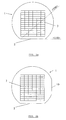
- Figure 1a describes the orientation of the dies on a standard ⁇ 100 ⁇ Si-wafer in standard processing.
- Figure 1b describes an alternative form of a standard ⁇ 100 ⁇ Si-wafer.
- Figure 1c shows an alternative pattern of devices on a standard wafer.
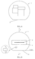
- Figure 2a shows a standard ⁇ 100 ⁇ Si-wafer with a long and narrow opening etched out.
- Figure 2b shows the wafer of figure 2a , after cleavage.
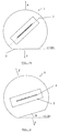
- Figure 3a shows a standard ⁇ 100 ⁇ Si-wafer wherein the device to be produced is tilted over an angle ⁇ with respect to the flat.
- Figure 4 shows a wafer wherein the device is parallel to the flat, but device and flat are tilted over an angle ⁇ with respect to ⁇ 110>.
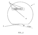
- Figure 5 shows a wafer wherein dies are printed using a step-and-repeat projection printing step in the photolithography.
- semiconductor wafers are mostly delivered in the form of circular shaped flat discs 1, with a straight edge or 'flat' 2 along a chord of the circular disc, said flat being used for positioning the wafer during processing.
- An additional straight edge 10 may be present, as shown in figure 1b , which is however shorter in length than the flat 2.
- the term 'flat' refers to the longest straight edge of a wafer.
- a wafer is partitioned into a number of 'dies' 3, which, after processing, will be separated to yield single chips.
- the partitioning into dies of equal dimensions is typical for devices produced on the basis of a projection printing process, such as step-and-repeat printing.
- Other printing processes such as those using a contact or proximity printer, allow other configurations, such as the one shown in figure 1c .
- the micromachining consists of producing a device 5 containing a long and narrow opening 4, from a wafer 1 with flat 2.
- the opening 4 may propagate, leading to breaking of the wafer. Breaking will occur along a so-called cleavage plane.
- the question whether or not the wafer will break and along which cleavage plane depends on the form of the opening, the stress applied, and on the orientation of the wafer's crystal structure with respect to the opening. It is the stress concentration around crack tips or other discontinuities which causes wafers to break even though they are subjected to an overall stress level, which is far below the material's yield strength.
- a stress intensity factor K is used, to numerically evaluate the eventuality of crack propagation.
- This will be illustrated (see figure 2a ) for the exemplary case of a tensile stress ⁇ in a silicon wafer, caused by external tensile forces F.
- the stress ⁇ is the tensile stress in the homogenous material, at a sufficiently large distance from the opening 4.
- the stress level will rise to very high local values, exceeding by far the value ⁇ in the homogenous material. This is why, at acceptable levels of the stress in the homogenous material, breaking of the wafer can be initiated at the edges of openings such as opening 4.
- silicon is a widely used material. It has excellent mechanical properties apart from significant photoelectric and thermoelectric effects and a reasonable carrier mobility.
- Standard Si-wafers are of the ⁇ 100 ⁇ type, meaning that their flat front and back surfaces are oriented along a plane belonging to the ⁇ 100 ⁇ family.
- the flat 2 is oriented along a ⁇ 110> direction which is the common intersection direction between on the one hand planes of the ⁇ 100 ⁇ and ⁇ 110 ⁇ families and on the other hand of planes of the ⁇ 100 ⁇ and ⁇ 111 ⁇ families.
- Figure 1a also shows the ⁇ 100> direction, which is the common intersection between on the one hand two planes of the ⁇ 100 ⁇ family and on the other hand planes of the ⁇ 100 ⁇ and ⁇ 110 ⁇ families.
- cleavage This means that the wafer breaks in two along a well defined cleavage plane that depends on the orientation of the stress with respect to the wafer's crystal structure.
- the flat of standard Si-wafers is oriented along the ⁇ 110> direction.
- the opening 4 is now parallel to said flat, as shown in figure 2a .
- Even a relatively low tensile stress ⁇ will cause a critical stress at the tip of the opening. If a critical stress level is reached, cleavage will occur along the line 6 of figure 2b .
- the cleavage plane depends on the orientation of the stress and the type of stress.
- a tensile stress or a bending stress may cause cleavage along a plane of the ⁇ 110 ⁇ or ⁇ 111 ⁇ families. This is because not only the K c factor is important, but also the projection of the stress perpendicular to the cleavage plane. To decrease the chance of cleavage along any of these planes, the present invention now proposes the following solutions.
- the present invention proposes a method of processing a wafer, wherein openings are etched at an angle ⁇ with respect to the direction ⁇ 110>, so that crack propagation is inhibited. More in particular, the longitudinal axis of the openings is at an angle ⁇ to said direction, the axis being defined as a straight line parallel to the wafer and to the longitudinal dimension of the openings. In the case of a rectangular opening, this axis is typically the rectangular's longest symmetry axis.
- Figure 2a shows the standard situation.
- the opening 4 is oriented along the ⁇ 110> direction.
- cleavage will occur as soon as a critical stress level is reached.
- Figure 3a shows a first alternative, whereby the device 5 and the opening 4 have been rotated over an angle ⁇ , with respect to ⁇ 110>.
- ⁇ depends on the material used. In the case of silicon for example, the orientation along ⁇ will decrease the chance of cleavage along one plane, but care must be taken that cleavage will not occur along another plane.
- the optimal value of ⁇ is lying between 0° and 45°: at 45°, the opening lies along the ⁇ 100> direction, which may lead to cleavage along another plane of the ⁇ 110 ⁇ family and along a line 7 shown in figure 3b .
- Figure 4 illustrates the second alternative, wherein the flat of the wafer is no longer oriented along the ⁇ 110>, but along a direction which is at an angle ⁇ with respect to that ⁇ 110> direction.
- the device 5 and the opening 4 remain parallel to the flat, as in the case of standard wafers.
- a wafer is subjected to a process comprising the steps of photolithography and etching, known in the art.
- the photolithography entails the printing of a pattern of dies, such as shown in figure 1a or 1c onto a wafer.
- This printing step may be performed in different ways.
- the pattern to be printed is produced on a so-called mask, to be placed between a light source and the wafer, in order to print the pattern onto said wafer.
- the mask is placed in contact with or very close to the wafer.
- contact or proximity printing which are used preferably to print a complete set of dies (as in figures 1a or 1c ).
- projection printing methods exist, whereby an optical system is employed between the mask and the wafer, which allows the printed pattern to be reduced in size with respect to the pattern on the mask.
- This last method is preferably used when a number of different dies with equal size are printed next to each other on the same wafer, a process also called step-and-repeat printing.
- openings are oriented on a standard wafer so that they are placed at an angle ⁇ with respect to the flat and thus to the ⁇ 110> direction.
- micromachined devices are produced by a method comprising the steps of photolithography and etching of a Si-wafer, wherein the photolithography step preferably comprises a contact or proximity printing step.
- the photolithography step preferably comprises a contact or proximity printing step.
- the mask can be rotated over that angle with respect to a stationary wafer, prior to photo-exposure of the pattern. This would of course require a printing device which allows such a rotation.
- the pattern on the mask may placed in a tilted position, at an angle ⁇ with respect to the mask, and then printed through the mask while the mask is in its standard position. This allows the use of a standard printing device.
- the wafer itself can be rotated over ⁇ , with respect to a stationary and standard printing device and standard mask.
- the wafer used in this embodiment of the invention is a standard wafer, with the flat oriented along the ⁇ 110> direction.
- openings are parallel to the flat, but the flat itself is tilted at an angle ⁇ with respect to the ⁇ 110> direction.
- This type of wafer is not standard and needs to be produced especially in this way.
- the production method of micromachined devices comprises equally the classic photolithography and etching steps, whereby the photolithography step may equally comprise a contact or proximity printing step.
- the tilted orientation of the flat with respect to the weaker ⁇ 110> direction permits the printing of the set of dies, according to standard processing methods, without necessitating the rotation of the mask, nor of the wafer.
- the method according to the second embodiment of the invention is especially suitable for a method wherein the photolithography is based on projection printing, such as step-and-repeat printing, as illustrated in figure 5 .
- this type of printing step is mostly used to acquire a set of dies 3 of identical dimensions, such as shown in figures 1a and 1b .
- the dies 3 are printed separately and consecutively onto the wafer 1.
- a standard wafer i.e.
Landscapes
- Engineering & Computer Science (AREA)
- Manufacturing & Machinery (AREA)
- Microelectronics & Electronic Packaging (AREA)
- Micromachines (AREA)
Description
- The present invention is related to a method for producing micromachined devices for use in Microelectromechanical Systems (MEMS). The present invention is also related to the devices obtained by said method and the use of said devices.
- In Microelectromechanical Systems (MEMS), also known as Microsystems or Micro Machined Systems, devices are often used, the production of which is based on the method technology developed in semiconductor processing, combined with specific MEMS technology. In MEMS technology, structures such as beams or cavities, can be added to micro-electronic circuitry. Compared to standard semiconductor devices, the mechanical properties of these micromachined devices are subject to very demanding criteria, in terms of breaking behaviour, weight, vibration resistance, etc, which is imposing higher standards on the processing of these devices.
- To produce certain types of micromachined devices, the method of bulk micromachining is used, wherein wells are etched in a semiconductor wafer, leaving membranes, openings or beams. This leads for example to pressure sensors, accelerometers, inclinometers, or optical devices.
- In the case of bulk micromachined accelerometers for example, openings are etched in the semiconductor wafer. Often, these openings are large and narrow, resembling elongated cracks in the wafer.
- In general, it is true that cavities or openings are formed in micromachined devices, which are large and deep in comparison to openings normally defined in semiconductor processing, such as contact or via holes, which have a diameter typically less than 5 µm and a depth less than 2µm. Such large openings or cavities are responsible for a weakening of the wafer and increase the chance of the wafer breaking under the influence of stresses induced for example during processing.
- It is known in the state of the art to exploit certain qualities related to the crystal structure of a semiconductor, in particular a Si wafer. For example, the etching of openings parallel to the <100> direction is beneficial in the case of anistropic wet etching steps. This is described in documents
EP-A-0658927 andUS-A-4969359 for example. However, narrow openings parallel to the <100> direction tend to weaken the wafer considerably, and increase the danger of unintended breaking by cleavage during processing. - In document
EP-A-0562880 , a semiconductor infra-red emitting device or LED on a substrate is described, the substrate being slanted with respect to the LED stack. The slanted orientation of the devices on the substrate is meant to obtain cleavage of the substrate in a predefined way. This document is not related to avoiding cleavage and thus mechanical failure, but to obtaining this cleavage. Neither is this document related to the production of MEMS, comprising openings or cavities. It is merely a way of dividing a wafer into separate devices by way of cleavage. The same is true of the documentDE-A-3435138 , which describes a way of obtaining single chips by cleavage, with a reduced risk of splitting a wafer along a second direction perpendicular to the intended direction. - Document
US-A-4278987 describes a semiconductor device prepared according to a method wherein a dent is etched and subsequently filled, said dent having a polygonal shape having main sides parallel to a direction along <100> or inclined within 25° with respect to <100>. The purpose for this slanted position is not for mechanical strength purposes, but for epitaxial growth and planarization purposes. Devices according to this document are not MEMS. - Document
JP-A-03219618 - The
US-A-4 969 359 is also relevant as prior art. - The present invention aims to provide a method for producing micromachined devices which have a higher resistance to crack propagation during and after processing.
- A further aim of the present invention is to provide micromachined devices having improved resistance to crack propagation.
- The present invention is related to a method for producing micromachined devices for use in Microelectromechanical Systems (MEMS), as defined in the appended claims.
- The present invention is related in particular to a method, wherein said wafer has the shape of a circular disc, with at least one part cut off along a chord of said circular disc, the longest of said chords being called 'the flat' of said wafer.
- According to a first preferred embodiment of the present invention, said flat is not parallel to said intersection.
- According to a second preferred embodiment of the present invention, said flat is parallel to said intersection.
- In the present invention, said wafer is a silicon wafer, whose front and back surfaces are oriented along a plane of the {100} family and wherein said cleavage plane is a plane belonging to the {111} or the {110} family. In these latter cases, said angle between said longitudinal axis of said opening and/or cavity and said direction is less than 44°.
- In the embodiment wherein said flat is oriented along said intersection, the method according to the invention comprises the steps of:
- subjecting said wafer to a photolithography step, whereby a pattern is printed through a mask onto said wafer,
- etching said wafer,
- According to the embodiment wherein said flat is oriented along said intersection, said photolithography step may comprise a contact printing step or a proximity printing step.
- In the embodiment wherein said flat is not oriented along said intersection, the method according to the invention comprises the steps of:
- subjecting said wafer to a photolithography step, whereby a pattern is printed through a mask onto said wafer,
- etching said wafer,
-
Figure 1a describes the orientation of the dies on a standard {100} Si-wafer in standard processing. -
Figure 1b describes an alternative form of a standard {100} Si-wafer. -
Figure 1c shows an alternative pattern of devices on a standard wafer. -
Figure 2a shows a standard {100} Si-wafer with a long and narrow opening etched out. -
Figure 2b shows the wafer offigure 2a , after cleavage. -
Figure 3a shows a standard {100} Si-wafer wherein the device to be produced is tilted over an angle θ with respect to the flat. -
Figure 3b shows the situation offig. 3a wherein θ = 45°. -
Figure 4 shows a wafer wherein the device is parallel to the flat, but device and flat are tilted over an angle θ with respect to <110>. -
Figure 5 shows a wafer wherein dies are printed using a step-and-repeat projection printing step in the photolithography. - As shown in
figure 1a , semiconductor wafers are mostly delivered in the form of circular shapedflat discs 1, with a straight edge or 'flat' 2 along a chord of the circular disc, said flat being used for positioning the wafer during processing. An additionalstraight edge 10 may be present, as shown infigure 1b , which is however shorter in length than the flat 2. In the following, the term 'flat' refers to the longest straight edge of a wafer. - In the case of standard semiconductor devices, a wafer is partitioned into a number of 'dies' 3, which, after processing, will be separated to yield single chips. The partitioning into dies of equal dimensions is typical for devices produced on the basis of a projection printing process, such as step-and-repeat printing. Other printing processes, such as those using a contact or proximity printer, allow other configurations, such as the one shown in
figure 1c . We will however base the following description on the exemplary case offigure 2a , wherein the micromachining consists of producing adevice 5 containing a long andnarrow opening 4, from awafer 1 with flat 2. - Under the influence of a load applied to the wafer, such as mechanical or thermal forces or shocks, the
opening 4 may propagate, leading to breaking of the wafer. Breaking will occur along a so-called cleavage plane. The question whether or not the wafer will break and along which cleavage plane, depends on the form of the opening, the stress applied, and on the orientation of the wafer's crystal structure with respect to the opening. It is the stress concentration around crack tips or other discontinuities which causes wafers to break even though they are subjected to an overall stress level, which is far below the material's yield strength. - In general, when a crack of length 2c is formed in a material, subjected to a stress σ in the homogenous material, a stress intensity factor K is used, to numerically evaluate the eventuality of crack propagation. This will be illustrated (see
figure 2a ) for the exemplary case of a tensile stress σ in a silicon wafer, caused by external tensile forces F. It is understood that the stress σ is the tensile stress in the homogenous material, at a sufficiently large distance from theopening 4. It is a known fact that in the vicinity of discontinuities (sharp edges, crack tips) the stress level will rise to very high local values, exceeding by far the value σ in the homogenous material. This is why, at acceptable levels of the stress in the homogenous material, breaking of the wafer can be initiated at the edges of openings such asopening 4. - This stress intensity factor K (expressed in MPA


- In micromachined devices, silicon is a widely used material. It has excellent mechanical properties apart from significant photoelectric and thermoelectric effects and a reasonable carrier mobility.
- Many of these properties are related to the crystalline structure of silicon. The atoms in a silicon wafer form a lattice structure, which, viewed from different angles reveals different patterns of atoms. The planes and directions in a Si-wafer are represented by their Miller indices, which are known in the art.
- Three families of planes: {100}, {110} and {111} are important in silicon wafers. Standard Si-wafers are of the {100} type, meaning that their flat front and back surfaces are oriented along a plane belonging to the {100} family. Also in standard Si-wafers, the flat 2 is oriented along a <110> direction which is the common intersection direction between on the one hand planes of the {100} and {110} families and on the other hand of planes of the {100} and {111} families.
Figure 1a also shows the <100> direction, which is the common intersection between on the one hand two planes of the {100} family and on the other hand planes of the {100} and {110} families. The failure of Si-wafers as a consequence of the stress concentrations described above, occurs by a phenomenon called cleavage: this means that the wafer breaks in two along a well defined cleavage plane that depends on the orientation of the stress with respect to the wafer's crystal structure. - In silicon, the value of Kc has been measured for cleavage along the three main Miller index plane families, resulting in the data of table 1 (P.J. Burnett, 'Properties of Silicon', EMIS datareview series no. 4, INSPEC, London, UK, 1988, p. 30). This can be interpreted as the likelihood of the wafer cleaving along a plane belonging to each of the three families mentioned.
- It is clear that the {100} family offers the most resistance to cleavage in the presence of a stress concentration, followed by {110} and {111} in that order. However, this doesn't mean that cleavage necessarily occurs along a plane of the {111} family, as will be explained after this.
- As stated above, the flat of standard Si-wafers is oriented along the <110> direction. Suppose that the
opening 4 is now parallel to said flat, as shown infigure 2a . Even a relatively low tensile stress σ, as shown infigure 2a , will cause a critical stress at the tip of the opening. If a critical stress level is reached, cleavage will occur along theline 6 offigure 2b . The cleavage plane depends on the orientation of the stress and the type of stress. A tensile stress or a bending stress may cause cleavage along a plane of the {110} or {111} families. This is because not only the Kc factor is important, but also the projection of the stress perpendicular to the cleavage plane. To decrease the chance of cleavage along any of these planes, the present invention now proposes the following solutions. - The present invention proposes a method of processing a wafer, wherein openings are etched at an angle θ with respect to the direction <110>, so that crack propagation is inhibited. More in particular, the longitudinal axis of the openings is at an angle θ to said direction, the axis being defined as a straight line parallel to the wafer and to the longitudinal dimension of the openings. In the case of a rectangular opening, this axis is typically the rectangular's longest symmetry axis.
-
Figure 2a shows the standard situation. Theopening 4 is oriented along the <110> direction. Under the influence of a tensile stress σ, perpendicular to <110>, cleavage will occur as soon as a critical stress level is reached. -
Figure 3a shows a first alternative, whereby thedevice 5 and theopening 4 have been rotated over an angle θ, with respect to <110>. Returning to the exemplary case of a tensile stress perpendicular to the flat, it is now the projection of the crack length 2c on the <110> direction which is to be taken into consideration in order to assess the chance of cleavage along the same plane as infigure 2b . - Such cleavage will now occur starting from a higher stress level σc':

factor 
figure 2b has diminished. - The optimal value of θ depends on the material used. In the case of silicon for example, the orientation along θ will decrease the chance of cleavage along one plane, but care must be taken that cleavage will not occur along another plane.
- This may happen when the projection of the stress on the direction perpendicular to the
opening 4, becomes high enough to initiate cleavage along another plane than the one that was 'reinforced' by tilting theopening 4. - For Si-wafers, the optimal value of θ is lying between 0° and 45°: at 45°, the opening lies along the <100> direction, which may lead to cleavage along another plane of the {110} family and along a
line 7 shown infigure 3b . -
Figure 4 illustrates the second alternative, wherein the flat of the wafer is no longer oriented along the <110>, but along a direction which is at an angle θ with respect to that <110> direction. Thedevice 5 and theopening 4 remain parallel to the flat, as in the case of standard wafers. - To have a similar situation than the previous, the wafer of
figure 4 is once again subjected to a tensile stress σ perpendicular to the flat. To assess the chance of the wafer breaking along the same cleavage plane as before, the relevant crack length to be taken into consideration is the projection of the real crack length 2c on the <110> direction. However, this projected length is now subjected to the projection of σ on the direction perpendicular to <110>. This means that cleavage will now occur when:

- In this case, the critical stress at which cleavage along the same plane as in
figure 2b occurs is further increased by afactor 1/cosθ. - Based on the two effects described above, two preferred embodiments of the method according to the invention are proposed. According to both embodiments, a wafer is subjected to a process comprising the steps of photolithography and etching, known in the art. The photolithography entails the printing of a pattern of dies, such as shown in
figure 1a or1c onto a wafer. This printing step may be performed in different ways. In all cases, the pattern to be printed is produced on a so-called mask, to be placed between a light source and the wafer, in order to print the pattern onto said wafer. In one type of printing, the mask is placed in contact with or very close to the wafer. This is called contact or proximity printing respectively, which are used preferably to print a complete set of dies (as infigures 1a or1c ). On the other hand, projection printing methods exist, whereby an optical system is employed between the mask and the wafer, which allows the printed pattern to be reduced in size with respect to the pattern on the mask. This last method is preferably used when a number of different dies with equal size are printed next to each other on the same wafer, a process also called step-and-repeat printing. - In a first preferred embodiment, illustrated in
figure 3a , openings are oriented on a standard wafer so that they are placed at an angle θ with respect to the flat and thus to the <110> direction. - According to this embodiment, micromachined devices are produced by a method comprising the steps of photolithography and etching of a Si-wafer, wherein the photolithography step preferably comprises a contact or proximity printing step. To acquire the tilting of the complete set of dies over an angle θ, different actions can be undertaken: the mask can be rotated over that angle with respect to a stationary wafer, prior to photo-exposure of the pattern. This would of course require a printing device which allows such a rotation. Alternatively, the pattern on the mask may placed in a tilted position, at an angle θ with respect to the mask, and then printed through the mask while the mask is in its standard position. This allows the use of a standard printing device. Finally, the wafer itself can be rotated over θ, with respect to a stationary and standard printing device and standard mask. The wafer used in this embodiment of the invention is a standard wafer, with the flat oriented along the <110> direction.
- In a second embodiment, illustrated in
figure 4 , openings are parallel to the flat, but the flat itself is tilted at an angle θ with respect to the <110> direction. This type of wafer is not standard and needs to be produced especially in this way. - According to this embodiment, the production method of micromachined devices comprises equally the classic photolithography and etching steps, whereby the photolithography step may equally comprise a contact or proximity printing step. The tilted orientation of the flat with respect to the weaker <110> direction, permits the printing of the set of dies, according to standard processing methods, without necessitating the rotation of the mask, nor of the wafer.
- Apart from that, the method according to the second embodiment of the invention is especially suitable for a method wherein the photolithography is based on projection printing, such as step-and-repeat printing, as illustrated in
figure 5 . As was stated before, this type of printing step is mostly used to acquire a set of dies 3 of identical dimensions, such as shown infigures 1a and 1b . In step-and-repeat printing, the dies 3 are printed separately and consecutively onto thewafer 1. To obtain an orientation of the die and/or the openings defined on it, on a standard wafer (i.e. with the flat parallel to <110>), it would be necessary to perform additional translation/rotation of the wafer between printing steps, in order to align the different dies, which would make the method more complex and time-consuming. With the wafer used in the method according to this embodiment, whereby the flat is not oriented along the <110> direction, the wafer can be processed in the classic way, without additional translation or rotation between printing steps.Table 1 Miller index plane {100} {110} {111} Kc 
0.95 0.9 0.82
Claims (13)
- A method for producing micromachined devices for use in Microelectromechanical Systems (MEMS), said devices having improved resistance to crack propagation, comprising the steps of:- providing a silicon wafer (1) whose front and back surfaces are oriented along a plane of the {100} family,- processing from said wafer at least one micromachined device (5) comprising at least one elongated opening and/or cavity, having a longitudinal axis, so that said longitunal axis is at an angle to a direction which lies along the intersection of the front plane of the wafer and a cleavage plane,characterized in that said cleavage plane is a plane belonging to the {111} or {110} family, and wherein said angle between said longitudinal axis of said opening and/or cavity and said intersection is more than 0 but less than 44°.
- A method according to claim 1, wherein said wafer (1) has the shape of a circular disc, with at least one part cut off along a chord of said circular disc, the longest of said chords being called 'the flat' (2) of said wafer.
- A method according to claim 2 wherein said flat (2) is not parallel to said intersection.
- A method according to claim 2, wherein said flat (2) is parallel to said intersection.
- A method according to claim 4, wherein said processing comprises the steps of :- subjecting said wafer (1) to a photolithography step, whereby a pattern is printed through a mask onto said waf er,- etching said wafer,characterised in that said photolithography step comprises the step of rotating said mask over an angle, with respect to said wafer.
- A method according to claim 4, wherein said processing comprises the steps of :- subjecting said wafer (1) to a photolithography step, whereby a pattern is printed through a mask onto said wafer,- etching said wafer,wherein said pattern is positioned at an angle with respect to said mask.
- A method according to claim 4, wherein said processing comprises the steps of :- subjecting said wafer to a photolithography step, whereby a pattern is printed through a mask onto said wafer,- etching said wafer,characterised in that said photolithography step comprises the step of rotating said wafer over an angle with respect to said mask.
- A method according to any one of claims 5 to 7, wherein said photolithography step comprises a contact printing step.
- A method according to any one of claims 5 to 7, wherein said photolithography step comprises a proximity printing step.
- A method according to claim 3, wherein said processing comprises the steps of:- subjecting said wafer to a photolithography step, whereby a pattern is printed through a mask onto said wafer,- etching said wafer.
- A method according to claim 10, wherein said photolithography step comprises a number of projection printing steps.
- A method according to claim 10, wherein said photolithography step comprises a contact printing step.
- A method according to claim 10, wherein said photolithography step comprises a proximiy printing step.
Priority Applications (1)
| Application Number | Priority Date | Filing Date | Title |
|---|---|---|---|
| EP20010870213 EP1201604B1 (en) | 2000-10-09 | 2001-10-08 | A method for producing micromachined devices |
Applications Claiming Priority (5)
| Application Number | Priority Date | Filing Date | Title |
|---|---|---|---|
| EP00870227 | 2000-10-09 | ||
| EP00870227A EP1195352A1 (en) | 2000-10-09 | 2000-10-09 | A method for producing micromachined devices and devices obtained thereof |
| US23922600P | 2000-10-10 | 2000-10-10 | |
| US239226P | 2000-10-10 | ||
| EP20010870213 EP1201604B1 (en) | 2000-10-09 | 2001-10-08 | A method for producing micromachined devices |
Publications (3)
| Publication Number | Publication Date |
|---|---|
| EP1201604A2 EP1201604A2 (en) | 2002-05-02 |
| EP1201604A3 EP1201604A3 (en) | 2006-04-12 |
| EP1201604B1 true EP1201604B1 (en) | 2010-04-07 |
Family
ID=27223775
Family Applications (1)
| Application Number | Title | Priority Date | Filing Date |
|---|---|---|---|
| EP20010870213 Expired - Lifetime EP1201604B1 (en) | 2000-10-09 | 2001-10-08 | A method for producing micromachined devices |
Country Status (1)
| Country | Link |
|---|---|
| EP (1) | EP1201604B1 (en) |
Family Cites Families (5)
| Publication number | Priority date | Publication date | Assignee | Title |
|---|---|---|---|---|
| US4278987A (en) * | 1977-10-17 | 1981-07-14 | Hitachi, Ltd. | Junction isolated IC with thick EPI portion having sides at least 20 degrees from (110) orientations |
| DE3435138A1 (en) * | 1984-09-25 | 1986-04-03 | Siemens AG, 1000 Berlin und 8000 München | Improvement to a method for separating semiconductor components which are obtained by breaking semiconductor wafers |
| US4969359A (en) * | 1989-04-06 | 1990-11-13 | Ford Motor Company | Silicon accelerometer responsive to three orthogonal force components and method for fabricating |
| DE4342767A1 (en) * | 1993-12-15 | 1995-06-22 | Ant Nachrichtentech | Method for producing a cuboid recess for receiving a component in a carrier plate |
| EP1130631A1 (en) * | 2000-02-29 | 2001-09-05 | STMicroelectronics S.r.l. | Process for forming a buried cavity in a semiconductor material wafer |
-
2001
- 2001-10-08 EP EP20010870213 patent/EP1201604B1/en not_active Expired - Lifetime
Also Published As
| Publication number | Publication date |
|---|---|
| EP1201604A2 (en) | 2002-05-02 |
| EP1201604A3 (en) | 2006-04-12 |
Similar Documents
| Publication | Publication Date | Title |
|---|---|---|
| US7808059B2 (en) | Semiconductor substrate, and semiconductor device and method of manufacturing the semiconductor device | |
| US6582985B2 (en) | SOI/glass process for forming thin silicon micromachined structures | |
| EP0228863B1 (en) | Method of dividing a substrate into a plurality of substrate portions | |
| Landesberger et al. | New dicing and thinning concept improves mechanical reliability of ultra thin silicon | |
| US4969359A (en) | Silicon accelerometer responsive to three orthogonal force components and method for fabricating | |
| US5154333A (en) | Jaw cleaving device | |
| US6740542B2 (en) | Method for producing micromachined devices and devices obtained thereof | |
| JPH0329310A (en) | Semiconductor wafer | |
| US10829412B2 (en) | Carriers for microelectronics fabrication | |
| KR102529797B1 (en) | Method of manufacturing light-emitting element | |
| JP2004186340A (en) | Cleaving method of compound semiconductor wafer | |
| EP1201604A2 (en) | A method for producing micromachined devices and devices obtained thereof | |
| EP1195352A1 (en) | A method for producing micromachined devices and devices obtained thereof | |
| CN101939129A (en) | Method for laser etching brittle components | |
| JPH08291000A (en) | Crystalline etching method | |
| KR20160026878A (en) | Method for designing tip shape for cutting member, method for manufacturing semiconductor dies, circuit board, and electronic device | |
| US6621149B2 (en) | Semiconductor chip production method and semiconductor wafer | |
| Oliver et al. | Diamond scribing and breaking of silicon for MEMS die separation | |
| US5307433A (en) | Optical connection member of silicon and method for the manufacture thereof | |
| KR100665517B1 (en) | Specimen and its manufacturing method for easy measurement of mechanical and fatigue properties of thin film materials | |
| EP1705153A2 (en) | Bevel dicing semiconductor components | |
| US20260011655A1 (en) | SiC SEMICONDUCTOR DEVICE AND METHOD OF MANUFACTURING THE SiC SEMICONDUCTOR DEVICE | |
| US20250381707A1 (en) | Method for manufacturing semiconductor wafers | |
| CN106466888B (en) | Vertical crack formation method and segmentation method in brittle material substrate | |
| CN118077035A (en) | Semiconductor devices |
Legal Events
| Date | Code | Title | Description |
|---|---|---|---|
| PUAI | Public reference made under article 153(3) epc to a published international application that has entered the european phase |
Free format text: ORIGINAL CODE: 0009012 |
|
| AK | Designated contracting states |
Kind code of ref document: A2 Designated state(s): AT BE CH CY DE DK ES FI FR GB GR IE IT LI LU MC NL PT SE TR |
|
| AX | Request for extension of the european patent |
Free format text: AL;LT;LV;MK;RO;SI |
|
| PUAL | Search report despatched |
Free format text: ORIGINAL CODE: 0009013 |
|
| AK | Designated contracting states |
Kind code of ref document: A3 Designated state(s): AT BE CH CY DE DK ES FI FR GB GR IE IT LI LU MC NL PT SE TR |
|
| AX | Request for extension of the european patent |
Extension state: AL LT LV MK RO SI |
|
| 17P | Request for examination filed |
Effective date: 20060907 |
|
| AKX | Designation fees paid |
Designated state(s): AT BE CH CY DE DK ES FI FR GB GR IE IT LI LU MC NL PT SE TR |
|
| 17Q | First examination report despatched |
Effective date: 20070109 |
|
| RAP1 | Party data changed (applicant data changed or rights of an application transferred) |
Owner name: EASTMAN KODAK COMPANY Owner name: IMEC |
|
| GRAP | Despatch of communication of intention to grant a patent |
Free format text: ORIGINAL CODE: EPIDOSNIGR1 |
|
| RTI1 | Title (correction) |
Free format text: A METHOD FOR PRODUCING MICROMACHINED DEVICES |
|
| GRAS | Grant fee paid |
Free format text: ORIGINAL CODE: EPIDOSNIGR3 |
|
| GRAA | (expected) grant |
Free format text: ORIGINAL CODE: 0009210 |
|
| AK | Designated contracting states |
Kind code of ref document: B1 Designated state(s): AT BE CH CY DE DK ES FI FR GB GR IE IT LI LU MC NL PT SE TR |
|
| REG | Reference to a national code |
Ref country code: GB Ref legal event code: FG4D |
|
| REG | Reference to a national code |
Ref country code: CH Ref legal event code: EP |
|
| REG | Reference to a national code |
Ref country code: IE Ref legal event code: FG4D |
|
| REF | Corresponds to: |
Ref document number: 60141737 Country of ref document: DE Date of ref document: 20100520 Kind code of ref document: P |
|
| REG | Reference to a national code |
Ref country code: NL Ref legal event code: VDEP Effective date: 20100407 |
|
| PG25 | Lapsed in a contracting state [announced via postgrant information from national office to epo] |
Ref country code: NL Free format text: LAPSE BECAUSE OF FAILURE TO SUBMIT A TRANSLATION OF THE DESCRIPTION OR TO PAY THE FEE WITHIN THE PRESCRIBED TIME-LIMIT Effective date: 20100407 Ref country code: ES Free format text: LAPSE BECAUSE OF FAILURE TO SUBMIT A TRANSLATION OF THE DESCRIPTION OR TO PAY THE FEE WITHIN THE PRESCRIBED TIME-LIMIT Effective date: 20100718 Ref country code: SE Free format text: LAPSE BECAUSE OF FAILURE TO SUBMIT A TRANSLATION OF THE DESCRIPTION OR TO PAY THE FEE WITHIN THE PRESCRIBED TIME-LIMIT Effective date: 20100407 |
|
| PG25 | Lapsed in a contracting state [announced via postgrant information from national office to epo] |
Ref country code: FI Free format text: LAPSE BECAUSE OF FAILURE TO SUBMIT A TRANSLATION OF THE DESCRIPTION OR TO PAY THE FEE WITHIN THE PRESCRIBED TIME-LIMIT Effective date: 20100407 Ref country code: AT Free format text: LAPSE BECAUSE OF FAILURE TO SUBMIT A TRANSLATION OF THE DESCRIPTION OR TO PAY THE FEE WITHIN THE PRESCRIBED TIME-LIMIT Effective date: 20100407 |
|
| PG25 | Lapsed in a contracting state [announced via postgrant information from national office to epo] |
Ref country code: GR Free format text: LAPSE BECAUSE OF FAILURE TO SUBMIT A TRANSLATION OF THE DESCRIPTION OR TO PAY THE FEE WITHIN THE PRESCRIBED TIME-LIMIT Effective date: 20100708 Ref country code: CY Free format text: LAPSE BECAUSE OF FAILURE TO SUBMIT A TRANSLATION OF THE DESCRIPTION OR TO PAY THE FEE WITHIN THE PRESCRIBED TIME-LIMIT Effective date: 20100407 |
|
| PG25 | Lapsed in a contracting state [announced via postgrant information from national office to epo] |
Ref country code: DK Free format text: LAPSE BECAUSE OF FAILURE TO SUBMIT A TRANSLATION OF THE DESCRIPTION OR TO PAY THE FEE WITHIN THE PRESCRIBED TIME-LIMIT Effective date: 20100407 Ref country code: PT Free format text: LAPSE BECAUSE OF FAILURE TO SUBMIT A TRANSLATION OF THE DESCRIPTION OR TO PAY THE FEE WITHIN THE PRESCRIBED TIME-LIMIT Effective date: 20100809 |
|
| PLBE | No opposition filed within time limit |
Free format text: ORIGINAL CODE: 0009261 |
|
| STAA | Information on the status of an ep patent application or granted ep patent |
Free format text: STATUS: NO OPPOSITION FILED WITHIN TIME LIMIT |
|
| PG25 | Lapsed in a contracting state [announced via postgrant information from national office to epo] |
Ref country code: BE Free format text: LAPSE BECAUSE OF FAILURE TO SUBMIT A TRANSLATION OF THE DESCRIPTION OR TO PAY THE FEE WITHIN THE PRESCRIBED TIME-LIMIT Effective date: 20100407 |
|
| 26N | No opposition filed |
Effective date: 20110110 |
|
| PG25 | Lapsed in a contracting state [announced via postgrant information from national office to epo] |
Ref country code: IT Free format text: LAPSE BECAUSE OF FAILURE TO SUBMIT A TRANSLATION OF THE DESCRIPTION OR TO PAY THE FEE WITHIN THE PRESCRIBED TIME-LIMIT Effective date: 20100407 |
|
| PG25 | Lapsed in a contracting state [announced via postgrant information from national office to epo] |
Ref country code: MC Free format text: LAPSE BECAUSE OF NON-PAYMENT OF DUE FEES Effective date: 20101031 |
|
| REG | Reference to a national code |
Ref country code: CH Ref legal event code: PL |
|
| PG25 | Lapsed in a contracting state [announced via postgrant information from national office to epo] |
Ref country code: CH Free format text: LAPSE BECAUSE OF NON-PAYMENT OF DUE FEES Effective date: 20101031 Ref country code: LI Free format text: LAPSE BECAUSE OF NON-PAYMENT OF DUE FEES Effective date: 20101031 |
|
| PG25 | Lapsed in a contracting state [announced via postgrant information from national office to epo] |
Ref country code: IE Free format text: LAPSE BECAUSE OF NON-PAYMENT OF DUE FEES Effective date: 20101008 |
|
| PG25 | Lapsed in a contracting state [announced via postgrant information from national office to epo] |
Ref country code: LU Free format text: LAPSE BECAUSE OF NON-PAYMENT OF DUE FEES Effective date: 20101008 |
|
| PG25 | Lapsed in a contracting state [announced via postgrant information from national office to epo] |
Ref country code: TR Free format text: LAPSE BECAUSE OF FAILURE TO SUBMIT A TRANSLATION OF THE DESCRIPTION OR TO PAY THE FEE WITHIN THE PRESCRIBED TIME-LIMIT Effective date: 20100407 |
|
| PGFP | Annual fee paid to national office [announced via postgrant information from national office to epo] |
Ref country code: GB Payment date: 20140924 Year of fee payment: 14 |
|
| PGFP | Annual fee paid to national office [announced via postgrant information from national office to epo] |
Ref country code: DE Payment date: 20140924 Year of fee payment: 14 Ref country code: FR Payment date: 20141021 Year of fee payment: 14 |
|
| REG | Reference to a national code |
Ref country code: DE Ref legal event code: R119 Ref document number: 60141737 Country of ref document: DE |
|
| GBPC | Gb: european patent ceased through non-payment of renewal fee |
Effective date: 20151008 |
|
| PG25 | Lapsed in a contracting state [announced via postgrant information from national office to epo] |
Ref country code: DE Free format text: LAPSE BECAUSE OF NON-PAYMENT OF DUE FEES Effective date: 20160503 Ref country code: GB Free format text: LAPSE BECAUSE OF NON-PAYMENT OF DUE FEES Effective date: 20151008 |
|
| REG | Reference to a national code |
Ref country code: FR Ref legal event code: ST Effective date: 20160630 |
|
| PG25 | Lapsed in a contracting state [announced via postgrant information from national office to epo] |
Ref country code: FR Free format text: LAPSE BECAUSE OF NON-PAYMENT OF DUE FEES Effective date: 20151102 |