EP1199806A2 - PLL circuit and optical communication reception apparatus - Google Patents
PLL circuit and optical communication reception apparatus Download PDFInfo
- Publication number
- EP1199806A2 EP1199806A2 EP01402709A EP01402709A EP1199806A2 EP 1199806 A2 EP1199806 A2 EP 1199806A2 EP 01402709 A EP01402709 A EP 01402709A EP 01402709 A EP01402709 A EP 01402709A EP 1199806 A2 EP1199806 A2 EP 1199806A2
- Authority
- EP
- European Patent Office
- Prior art keywords
- signal
- level
- circuit
- frequency
- input
- Prior art date
- Legal status (The legal status is an assumption and is not a legal conclusion. Google has not performed a legal analysis and makes no representation as to the accuracy of the status listed.)
- Granted
Links
Images








Classifications
-
- H—ELECTRICITY
- H03—ELECTRONIC CIRCUITRY
- H03D—DEMODULATION OR TRANSFERENCE OF MODULATION FROM ONE CARRIER TO ANOTHER
- H03D13/00—Circuits for comparing the phase or frequency of two mutually-independent oscillations
- H03D13/003—Circuits for comparing the phase or frequency of two mutually-independent oscillations in which both oscillations are converted by logic means into pulses which are applied to filtering or integrating means
- H03D13/004—Circuits for comparing the phase or frequency of two mutually-independent oscillations in which both oscillations are converted by logic means into pulses which are applied to filtering or integrating means the logic means delivering pulses at more than one terminal, e.g. up and down pulses
-
- H—ELECTRICITY
- H03—ELECTRONIC CIRCUITRY
- H03L—AUTOMATIC CONTROL, STARTING, SYNCHRONISATION OR STABILISATION OF GENERATORS OF ELECTRONIC OSCILLATIONS OR PULSES
- H03L7/00—Automatic control of frequency or phase; Synchronisation
- H03L7/06—Automatic control of frequency or phase; Synchronisation using a reference signal applied to a frequency- or phase-locked loop
- H03L7/08—Details of the phase-locked loop
- H03L7/085—Details of the phase-locked loop concerning mainly the frequency- or phase-detection arrangement including the filtering or amplification of its output signal
- H03L7/087—Details of the phase-locked loop concerning mainly the frequency- or phase-detection arrangement including the filtering or amplification of its output signal using at least two phase detectors or a frequency and phase detector in the loop
-
- H—ELECTRICITY
- H03—ELECTRONIC CIRCUITRY
- H03L—AUTOMATIC CONTROL, STARTING, SYNCHRONISATION OR STABILISATION OF GENERATORS OF ELECTRONIC OSCILLATIONS OR PULSES
- H03L7/00—Automatic control of frequency or phase; Synchronisation
- H03L7/06—Automatic control of frequency or phase; Synchronisation using a reference signal applied to a frequency- or phase-locked loop
- H03L7/16—Indirect frequency synthesis, i.e. generating a desired one of a number of predetermined frequencies using a frequency- or phase-locked loop
- H03L7/18—Indirect frequency synthesis, i.e. generating a desired one of a number of predetermined frequencies using a frequency- or phase-locked loop using a frequency divider or counter in the loop
- H03L7/183—Indirect frequency synthesis, i.e. generating a desired one of a number of predetermined frequencies using a frequency- or phase-locked loop using a frequency divider or counter in the loop a time difference being used for locking the loop, the counter counting between fixed numbers or the frequency divider dividing by a fixed number
- H03L7/191—Indirect frequency synthesis, i.e. generating a desired one of a number of predetermined frequencies using a frequency- or phase-locked loop using a frequency divider or counter in the loop a time difference being used for locking the loop, the counter counting between fixed numbers or the frequency divider dividing by a fixed number using at least two different signals from the frequency divider or the counter for determining the time difference
-
- H—ELECTRICITY
- H03—ELECTRONIC CIRCUITRY
- H03L—AUTOMATIC CONTROL, STARTING, SYNCHRONISATION OR STABILISATION OF GENERATORS OF ELECTRONIC OSCILLATIONS OR PULSES
- H03L7/00—Automatic control of frequency or phase; Synchronisation
- H03L7/06—Automatic control of frequency or phase; Synchronisation using a reference signal applied to a frequency- or phase-locked loop
- H03L7/08—Details of the phase-locked loop
- H03L7/085—Details of the phase-locked loop concerning mainly the frequency- or phase-detection arrangement including the filtering or amplification of its output signal
- H03L7/089—Details of the phase-locked loop concerning mainly the frequency- or phase-detection arrangement including the filtering or amplification of its output signal the phase or frequency detector generating up-down pulses
- H03L7/0891—Details of the phase-locked loop concerning mainly the frequency- or phase-detection arrangement including the filtering or amplification of its output signal the phase or frequency detector generating up-down pulses the up-down pulses controlling source and sink current generators, e.g. a charge pump
-
- H—ELECTRICITY
- H04—ELECTRIC COMMUNICATION TECHNIQUE
- H04L—TRANSMISSION OF DIGITAL INFORMATION, e.g. TELEGRAPHIC COMMUNICATION
- H04L7/00—Arrangements for synchronising receiver with transmitter
- H04L7/02—Speed or phase control by the received code signals, the signals containing no special synchronisation information
- H04L7/033—Speed or phase control by the received code signals, the signals containing no special synchronisation information using the transitions of the received signal to control the phase of the synchronising-signal-generating means, e.g. using a phase-locked loop
Definitions
- This invention relates to a PLL (Phase Locked Loop) circuit and an optical communication reception apparatus, and more particularly to a PLL circuit which includes a phase detection circuit and a frequency detection circuit and an optical communication reception apparatus which uses a PLL circuit as a production circuit for a clock signal to be used for retiming processing of receive data.
- PLL Phase Locked Loop
- FIG. 14 shows a configuration of a PLL circuit which is used commonly.
- the PLL circuit shown includes a phase detection (PD) circuit 101 and a frequency detection (FD) circuit 102 and operates in the following manner.
- PD phase detection
- FD frequency detection
- the frequency detection circuit 102 performs phase comparison between an input signal DATA and clock signals (ICLK, QCLK). Then, the frequency of a frequency clock VCOCLK of a voltage-controlled oscillator (VCO) 106 is controlled through a charge pump (CP) circuit 104 and a loop filter 105 based on a result of the comparison to pull the oscillation frequency of the VCO 106 to a target oscillation frequency.
- the clock signals (ICLK, QCLK) are produced based on the oscillation frequency clock VCOCLK of the VCO 106 by a clock generator 107.
- the phase detection circuit 101 performs phase comparison between the input signal DATA and the oscillation frequency clock VCOCLK of the VCO 106. Then, the phase detection circuit 101 controls the phase of the frequency clock VCOCLK of the VCO 106 through another charge pump circuit 103 and the loop filter 105 based on a result of the comparison to cause the phase of the frequency clock VCOCLK of the VCO 106 with the phase of the input signal DATA
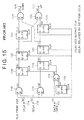
- a frequency comparison circuit of such a configuration as shown in FIG. 15 is conventionally used for the frequency detection circuit 102.
- a detailed circuit configuration and operation of the frequency detection circuit 102 are described.
- n 1
- an ICLK input terminal 114 to which the clock signal ICLK is inputted is connected to an input terminal A of each of a pair of AND gates 116 and 117 while a QCLK input terminal 115 to which the clock signal QCLK is inputted is connected to the other input terminals B of the AND gates 116 and 117.
- the input terminal A of the AND gate 117 is a negated input terminal through which the clock signal ICLK is inputted with the reversed polarity.
- the output terminals of the AND gates 116 and 117 are connected to the D input terminals of D-FFs 118 and 119, respectively.
- the output terminal of the EX-OR gate 113 is connected to the CLK input terminals of the D-FFs 118 and 119.
- the Q output terminals of the D-FFs 118 and 119 are connected to the D input terminals of D-FFs 120 and 121, and the Q output terminals of the D-FFs 120 and 121 are connected to the D input terminals of D-FFs 122 and 123, respectively.
- the CLK terminals of the D-FF 112 and the D-FFs 120 to 123 are connected to the ICLK input terminal 114.
- the Q output terminal of the D-FF 122 is connected to an input terminal A of an AND gate 124.
- the Q output terminal of the D-FF 123 is connected to an input terminal B of another AND gate 125.
- the Q output terminal of the D-FF 120 is further connected to an input terminal A of the AND gate 125, and the Q output terminal of the D-FF 121 is connected to an input terminal B of the AND gate 124.
- the output terminals of the AND gates 124 and 125 are connected to circuit output terminals 126 and 127, respectively.
- a DOWN pulse signal for controlling the VCO 106 of FIG. 14 to lower the oscillation frequency of it is extracted as an output signal from the AND gate 124 while an UP pulse signal for controlling the VCO 106 to raise the oscillation frequency is extracted as an output signal from the AND gate 125.
- the DOWN pulse signal and the UP pulse signal are supplied to the charge pump circuit 104 of FIG. 14 through the circuit output terminals 126 and 127, respectively.
- waveforms (a) to (o) indicate waveforms at nodes (a) to (o) of FIG. 15, respectively.
- the clock signal ICLK (a) has a pulse waveform wherein it rises to the "H” (high) level at time t0 and falls to the "L” (low) level at time t2. Similarly, the clock signal ICLK (a) rises at times t4, t8, t12, ... and falls at times t6, t10, ....
- the clock signal ICLK (a) is supplied to the input terminals A of the AND gates 116 and 117 through the ICLK input terminal 114 and supplied also to the CLK terminals of the D-FF 112 and the D-FFs 120 to 123.
- the clock signal QCLK (b) has a pulse waveform having a phase shifted by 90 degrees, more particularly, delayed by 90 degrees with respect to the clock signal ICLK (a).
- the clock signal QCLK (b) rises to the "H" level at times t1, t5, t9, ... and falls to the "L” level at times t3, t7, t11, ....
- the clock signal QCLK (b) is supplied to the input terminals B of the AND gates 116 and 117.
- the AND gate 116 logically ANDs the clock signal ICLK (a) and the clock signal QCLK (b). Therefore, the output signal (c) of the AND gate 116 exhibits the "H" level within those periods within which both of the clock signals ICLK and QCLK have the "H” level, that is, within the period from time t1 to time t2, the period from time t5 to time t6 and the period from time t9 to time t10.
- the output signal (c) of the AND gate 116 exhibits the "L" level.
- the AND gate 117 logically ANDs the inverted clock signal ICLKX of the clock signal ICLK (a) and the clock signal QCLK (b). Therefore, the output signal (d) of the AND gate 117 exhibits the "H" level within those periods within which both of the clock signals ICLKX and QCLK have the "H” level, that is, within the period from time t2 to time t3, the period from time t6 to time t7 and the period from time t10 to time t11.
- the output signal (d) of the AND gate 117 exhibits the "L" level.
- the period within which the output signal (c) exhibits the "H” level is represented as a period A while the period within which the output signal (d) exhibits the "H” level is represented as a period B.
- the NRZ input signal DATA (f) is supplied immediately to the input terminal A of the EX-OR gate 113 through the data input terminal 111 and supplied also to the D input terminal of the D-FF 112.
- the D-FF 112 fetches the "H" level/"L” level of the input waveform to the D input terminal at the timing of a rising edge of the clock signal ICLK (a). In this instance, if the input signal DATA (f) has the "H" level at time t0, then since the D-FF 112 fetches this, the level of the Q output signal (e) thereof changes to the "H" level.
- the D-FF 112 fetches the input signal DATA (f) of the "L” level and changes its Q output signal (e) to the "L” level at the timing of a next rising edge of the clock signal ICLK (a). Further, since the polarity of the input signal DATA (f) reverses again between times t6 and t7, the D-FF 112 fetches the input signal DATA (f) of the "H” level at the next rising timing t8 of the clock signal ICLK (a) and changes its Q output signal (e) to the "H” level. Thereafter, the D-FF 112 keeps the "H” level till time t12.
- the Q output signal (e) of the D-FF 112 is supplied to the input terminal B of the EX-OR gate 113.
- the EX-OR gate 113 exclusively ORs the Q output signal (e) supplied to the input terminal B and the input signal DATA (f) supplied to the input terminal A.
- the level of the output signal (g) of the EX-OR gate 113 changes from the "L" level to the "H” level when the input signal DATA (f) reverses during the period from time t1 to time t2, and changes back to the "L” level at time t4 at which the Q output signal (e) of the D-FF 112 exhibits a level change to the "L” level.
- the output signal (g) of the EX-OR gate 113 maintains the "L” level. Then, when the input signal DATA (f) reverses within the period from time t6 to time t7, the output signal (g) of the EX-OR gate 113 exhibits a level change from the "L” level to the "H” level at the timing of the reversal.
- the level of the Q output signal (e) of the D-FF 112 changes from the "L” level to the "H” level. Consequently, the EX-OR gate 113 logically ORs the "H” level of the input signal DATA (f) and the "H” level of the Q output signal (e), and therefore, the level of the output signal (g) of the EX-OR gate 113 changes to the "L” level. Then, within the following period from time t8 to time t12, the level of the output signal (g) of the EX-OR gate 113 does not exhibit a change.
- the output signals (c) and (d) of the AND gates 116 and 117 are inputted to the D input terminals of the D-FFs 118 and 119 in the next stage, respectively.
- the D-FFs 118 and 119 receive the output signal (g) of the EX-OR gate 113 as inputs to the CLK terminals thereof, and fetch the D input waveforms at the timing of a rising edge of the clock waveform and output the fetched levels as the Q output signals (h) and (k), respectively.
- the output signal (g) of the EX-OR gate 113 rises within the period from time t1 to time t2 and, within the period, the output signal (c) of the AND gate 116 has the "H” level and the output signal (d) of the AND gate 117 has the "L” level, the Q output signal (h) of the D-FF 118 exhibits the "H” level and the Q output signal (k) of the D-FF 119 exhibits the "L” level.
- the timing at which the level of the output signal (g) of the EX-OR gate 113 changes from the "L” level to the "H” level is a changing point of the input signal DATA (f) within the period from time t6 to time t7. Since the output signal (c) of the AND gate 116 has the “L” level and the output signal (d) of the AND gate 117 has the "H” level at the timing, the level of the Q output signal (h) of the D-FF 118 changes from the "H” level to the "L” level and the level of the Q output signal (k) of the D-FF 119 changes from the "L” level to the “H” level. Thereafter, the levels are maintained till time t12.
- the Q output signals (h) and (k) of the D-FFs 118 and 119 are supplied to the D input terminals of the D-FFs 120 and 121, respectively.
- the D-FFs 120 and 121 receive the clock signal ICLK (a) as the CLK inputs thereto and fetch the D input waveforms at the timing of a rising edge of the waveform of the clock signal ICLK (a).
- the timing of the rising edge of the clock signal ICLK (a) is time t4
- the Q output signal (h) of the D-FF 118 has the "H” level and the Q output signal (k) of the D-FF 119 has the "L” level at the timing
- the level of the Q output signal (i) of the D-FF 120 becomes the "H” level
- the level of the Q output signal (l) of the D-FF 121 becomes the "L" level.
- the next rising edge timing of the clock signal ICLK (a) is time t8 and the Q output signal (h) of the D-FF 118 has the "L” level then. Therefore, the level of the Q output signal (i) of the D-FF 120 changes to the "L” level. Meanwhile, since the level of the Q output signal (k) of the D-FF 119 is the "H” level, the level of the Q output signal (l) of the D-FF 121 changes to the "H” level. The levels of the Q output signals (i) and (l) are maintained till time t12.
- the Q output signals (i) and (l) of the D-FFs 120 and 121 are inputted to the D input terminals of the D-FFs 122 and 123 in the next stage, respectively.
- the D-FFs 122 and 123 receive the clock signal ICLK (a) as the CLK inputs thereto and fetch the D input waveforms at the timing of a rising edge of the waveform.
- the rising edge timing of the clock signal ICLK (a) is time t8 and the D-FFs 122 and 123 fetch the levels of the Q output signals (i) and (l) of the D-FFs 120 and 121, respectively. Consequently, the level of the Q output signal (j) of the D-FF 122 changes to the "H” level and the level of the Q output signal (m) of the D-FF 123 changes to the "L" level.
- the timing at which the clock signal ICLK (a) rises subsequently is time t12, and the Q output signal (i) of the D-FF 120 has the “L” level and the Q output signal (l) of the D-FF 121 has the "H” level at the timing. Therefore, the level of the Q output signal (j) of the D-FF 122 changes from the “H” level to the "L” level while the level of the Q output signal (m) of the D-FF 123 changes from the "L" level to the "H” level.
- the Q output signal (j) of the D-FF 122 is supplied to the input terminal A of the AND gate 124.
- the Q output signal (l) of the D-FF 121 is supplied to the input terminal B of the AND gate 124. Consequently, the level of the DOWN pulse signal which is the output signal (n) of the AND gate 124 changes to the "L” level because the Q output signal (l) of the D-FF 121 changes to the "L” level at time t4. Then, at time t8, since both of the levels of the Q output signals (l) and (j) of the D-FFs 121 and 122 change to the "H" level, the level of the DOWN pulse signal changes to the "H" level.
- the level of the Q output signal (l) of the D-FF 121 since the level of the Q output signal (l) of the D-FF 121 does not change and remains at the "H” level, the level of the Q output signal (j) of the D-FF 122 changes from the "H” level to the "L” level. Accordingly, the level of the output signal (n) of the AND gate 124, that is, the level of the DOWN pulse signal, changes from the "H" level to the "L” level.
- the Q output signal (m) of the D-FF 123 is supplied to the input terminal B of the AND gate 125.
- the Q output signal (i) of the D-FF 120 is supplied to the input terminal A of the AND gate 125. Consequently, the UP pulse signal which is the output signal (o) of the AND gate 125 exhibits the "L” level because the levels of the Q output signals (i) and (m) of the D-FFs 120 and 123 change to the "L" level at time t8. Then at time t12, the level of the Q output signal (m) of the D-FF 123 changes to the "H” level. However, since the level of the Q output signal (i) of the D-FF 120 remains at the "L” level, the output signal (o) of the AND gate 125 maintains the "L” level.
- an UP pulse signal of a duration equal to one period of the clock signal ICLK is outputted.
- data of m bits (m is an arbitrary integer) is present between the two DATA changing points of time, then since this signifies that less than m cycles of the clock signal ICLK are present within the period, in order to raise the frequency of the clock signal ICLK, a pulse or pulses of the UP pulse signal are produced.
- the output signal (n) of the AND gate 124 is supplied as the DOWN pulse signal and the output signal (o) of the AND gate 125 is supplied as the UP pulse signal to the charge pump circuit 104 of the charge pump circuit 104.
- the DOWN/UP pulse signal is used to control the charge pump circuit 104 to smooth (rectify) the output current of the charge pump circuit 104 to generate a control voltage for the VCO 106 through the loop filter 105.
- the operation of the frequency detection circuit 102 in the foregoing description relates to operation when the duty ratios of the input signal DATA and the clock signals (ICLK and QCLK) are 100 % and 50 %, respectively.
- the transmission signal DATA suffers from some duty distortion as seen from the waveform (b) or (c) of FIG. 17, and this may possibly give rise to malfunction of the PLL circuit.
- FIG. 18 illustrates waveforms of the clock signals ICLK and QCLK and the transmission signal DATA when they suffer from some duty distortion.
- the values of the clock signal ICLK and the clock signal QCLK are sampled at a changing point of time of the input signal DATA. Therefore, if the frequencies of the signals coincide fully with one each other, then the sample value within the period from time t2 to time t3 in FIG.
- the clock signal QCLK is obtained by delaying the phase of the clock signal ICLK by 90 degrees, if the duty ratio of the input signal DATA increases and the width for one bit of the "H" level thereof becomes greater than the period of the clock signal ICLK, then if the input signal DATA rises within the period from time t1 to time t2, then the level of the clock signal ICLK is "1” and the level of the clock signal QCLK is "1" at the rising edge of the input signal DATA.
- FIG. 19 shows an example of a circuit configuration of the phase detection circuit 101.
- a data input terminal 131 to which the input signal DATA is supplied is connected to the D input terminal of a D-FF 133 and connected also to an input terminal A of a 2-input exclusive OR (EX-OR) gate 135.
- a CLK input terminal 132 to which the oscillation frequency clock VCOCLK of the VCO 106 is connected to the CLK terminal of a D-FF 133 and connected also to a negated CLK terminal of a D-FF 134.
- the Q output terminal of the D-FF 133 is connected to the other input terminal B of the EX-OR gate 135, an input terminal A of a 2-input EX-OR gate 136, and the D input terminal of the D-FF 134.
- the Q output terminal of the D-FF 134 is connected to the other input terminal B of the EX-OR gate 136.
- the output terminal of the EX-OR gate 135 is connected to an UP output terminal 137 while the output terminal of the EX-OR gate 136 is connected to a DOWN output terminal 138.
- waveforms (a) to (f) represent waveforms at nodes (a) to (f) of FIG. 19, respectively.
- the waveform of the input signal DATA (b) falls between times t1 and t2 and rises between times t5 and t6 and thus keeps the “L” level within the period between the falling and rising edges; it falls between times t8 and t9 and keeps the "H” level within the period between the preceding rising edge and the falling edge; it rises between times t10 and t11 and keeps the “L” level within the period between the preceding falling edge and the rising edge; it falls between times t12 and t13 and keeps the "H” level within the period between the preceding rising edge and the falling edge; and it thereafter keeps the "L” level till time t15.
- the D-FF 133 fetches the "L” level of the input signal DATA (b) at the rising timing t2 of the oscillation frequency clock VCOCLK (a). Consequently, the level of the Q output signal (c) of the D-FF 133 changes to the "L” level.
- the input signal DATA does not exhibit a change and remains in the "L” level, and therefore, also the Q output signal (c) of the D-FF 133 does not exhibit a change but maintains the "L” level.
- the level of the Q output signal (c) of the D-FF 133 changes to the "H” level. Further, at the rising timing of the oscillation frequency clock VCOCLK (a) at time t8, the input signal DATA has the "H” level, and since the D-FF 133 fetches the "H” level of the input signal DATA, the Q output signal (c) of the D-FF 133 does not exhibit a change but remains in the "H” level.
- the level of the input signal DATA has the "L” level
- the level of the Q output signal (c) of the D-FF 133 changes from the "H” level to the “L” level.
- the level of the Q output signal (c) of the D-FF 133 changes to the "H” level, and then at time the next rising timing t14 of the oscillation frequency clock VCOCLK (a), the input signal DATA has the "L” level. Consequently, the D-FF 133 fetches the "L” level of the input signal DATA, and the level of the Q output signal (c) of the D-FF 133 changes to the "L” level.
- the oscillation frequency clock VCOCLK (a) is supplied in an inverted form as a CLK input to the D-FF 134. Accordingly, the D-FF 134 fetches the input signal DATA at times t1, t3, t5, t7, t9, t11, t13 and t15 at which the oscillation frequency clock VCOCLK (a) falls.
- the Q output signal (c) of the D-FF 133 since the Q output signal (c) of the D-FF 133 has the "H” level, the level of the Q output signal (d) of the D-FF 134 changes to the "H” level, and the "H” level is maintained till the next falling timing t3 of the oscillation frequency clock VCOCLK (a).
- the D-FF 134 fetches the "L” level and the level of the Q output signal (d) thereof changes from the "H” level to the "L” level. Then, the Q output signal (d) maintains the "L” level till immediately before time t7 past time t5.
- the D-FF 134 fetches the "H” level, and consequently, the level of the Q output signal (d) of the D-FF 134 changes to the "H” level.
- the level of the Q output signal (c) of the D-FF 133 does not change at time t9 but changes to the "L" level at time t10, and maintains the "L” level till time t12.
- the Q output signal (c) of the D-FF 133 has the "L” level, and the D-FF 134 fetches the "L” level. Therefore, the Q output signal (d) of the D-FF 134 changes from the "H" level to the "L” level.
- the D-FF 134 fetches the "H” level and the level of the Q output signal (d) of the D-FF 134 changes from the "L” level to the "H” level.
- the information of the "H” level is maintained till the next falling timing t15 of the oscillation frequency clock VCOCLK (a), at which the "L” level of the Q output signal (c) of the D-FF 133 is fetched into the D-FF 134. Consequently, the level of the Q output signal (d) of the D-FF 134 changes from the "H” level to the "L” level.
- the logical values of the input signal DATA (b) and the Q output signal (c) of the D-FF 133 are different from each other within the period from a point of time at which the level of the input signal DATA (b) changes from the "H” level to the "L” level between times t1 and t2 to time t2 at which the Q output signal (c) of the D-FF 133 has the "H” level, within the period from a point of time at which the level of the input signal DATA (b) changes from the "L” level to the "H” level between times t5 and t6 to time t6 at which the level of the Q output signal (c) of the D-FF 133 changes from the "L” level to the "H” level, within the period from a point of time at which the level of the input signal DATA (b) changes from the "H” level to the "L” level between times t8 and t9 to time t10, within the period from a point of time at which the level of the input signal
- the output signal (e) of the EX-OR gate 135 exhibits the "H” level.
- the output signal (e) of the 2-input EX-OR gate 135 exhibits the "L” level and is used as the UP pulse signal.
- the logical values of the Q output signal (c) of the D-FF 133 and the Q output signal (d) of the D-FF 134 are different from each other within the period from time t2 to time t3, the period from time t6 to time t7, the period from time t10 to time t11, the period from time t12 to time t13 and the period from time t14 to time t15.
- the DOWN pulse signal (f) of the EX-OR gate 136 exhibits the "H” level.
- the DOWN pulse signal (f) of the EX-OR gate 136 exhibits the "L” level and is used as the DOWN pulse signal.
- the pulse waveforms of the UP pulse signal (e) and the DOWN pulse signal (f) are generated each by one time.
- the pulse width of the DOWN pulse signal (f) is normally fixed, and phase control is performed by adjusting the pulse width of the UP pulse signal (e).
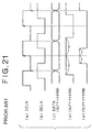
- the oscillation frequency clock VCOCLK of the VCO 106 is locked to the input signal DATA by control based on the control signals (UP pulse signal/DOWN pulse signal) of the frequency detection circuit 102 and the phase detection circuit 101, then the rising timing of the clock signal ICLK is positioned at the center of the eye pattern of the input signal DATA as seen from the timing chart of FIG. 21.
- the frequency detection circuit 102 samples the values (levels) of the clock signal ICLK and the clock signal QCLK at each changing point of the input signal DATA and uses the sample value to obtain frequency information.
- the clock signal ICLK and the input signal DATA have such a phase relationship with each other as seen in FIG. 21, then a falling timing of the clock signal ICLK and a changing point of the input signal DATA become a substantially same point of time.
- the sample value of the clock signal ICLK at a changing point of the input signal DATA by the frequency detection circuit 102 with respect to a change of the duty ratio of the input signal DATA becomes unstable (however, the sample value of the clock signal QCLK is stable when compared with that of the clock signal ICLK).
- the frequency detection circuit 102 detects the frequency information but in error and generates a wrong control signal.
- the frequency detection circuit 102 samples the clock signal ICLK and the clock signal QCLK at each changing point of the input signal DATA, when the input signal DATA has some duty distortion, a wrong control signal (UP pulse signal/DOWN pulse signal) is outputted from the frequency detection circuit 102.
- the frequency clock VCOCLK of the VCO 106 is locked to the input signal DATA, since the center of the eye pattern of the input signal DATA is positioned at a rising edge of the clock signal ICLK by action of the phase detection circuit 101, the sample value of the clock signal ICLK by the frequency detection circuit 102 with respect to a small change of the duty ratio of the input signal DATA becomes unstable, and a wrong control signal is outputted from the frequency detection circuit 102.
- a PLL circuit comprising an oscillator for generating an oscillation frequency signal having a variable oscillation frequency, a signal generation circuit for generating, based on the oscillation frequency signal of the oscillator, a first signal having a phase same as that of the oscillation frequency signal, a second signal having a fixed phase difference from the first signal, and a third signal having a phase difference smaller than the phase difference between the first and second signals from the first signal, a phase detection circuit for comparing the phases of the third signal generated by the signal generation circuit and an input signal and outputting, based on a result of the comparison, a first phase control signal for advancing the phase of the oscillation frequency signal of the oscillator or a second phase control signal for delaying the phase of the oscillation frequency signal of the oscillator, and a frequency detection circuit for fetching the first and second signals generated by the signal generation circuit in synchronism with the input signal and outputting, based on the fetched
- an optical communication reception apparatus comprising light reception means for receiving an optical signal, converting the optical signal into an electric signal and outputting the electric signal, a PLL circuit for producing a clock signal synchronized with the output signal of the light reception means, and a retiming circuit for retiming the output signal of the light reception means based on the clock signal produced by the PLL circuit, the PLL circuit including an oscillator for generating an oscillation frequency signal having a variable oscillation frequency, a signal generation circuit for generating, based on the oscillation frequency signal of the oscillator, a first signal having a phase same as that of the oscillation frequency signal, a second signal having a fixed phase difference from the first signal, and a third signal having a phase difference smaller than the phase difference between the first and second signals from the first signal, a phase detection circuit for comparing the phases of the third signal generated by the signal generation circuit and an input signal and outputting, based on a result of the comparison, a first phase control signal for
- the signal generation circuit generates, based on the oscillation frequency signal of the oscillator, a first signal having a phase same as that of the oscillation frequency signal, a second signal having a fixed phase difference from the first signal, and a third signal having a phase difference smaller than the phase difference between the first and second signals from the first signal, and the phase detection circuit performs phase control based on the phase difference between the third signal and the input signal. Consequently, a changing point of the third signal is set not to a changing point of the input signal but to a central portion of the pulse waveform.
- the frequency detection circuit has an improved withstanding property against a metastable state which appears when the duty ratio of the input signal varies at a fetching timing of the first or second signal when the oscillation frequency is in the proximity of a particular frequency to which the oscillator is locked. Accordingly, even if the duty ratio of the input signal changes, the convergence time required for frequency detection of the frequency detection circuit is short and a malfunction with the control signal of the frequency detection circuit is less likely to occur. Therefore, operation of the entire PLL circuit is stabilized.
- FIG. 1 there is shown an example of a configuration of a PLL circuit to which the present invention is applied.
- the PLL circuit shown is used, for example, in a reception apparatus for optical communication although it can be applied to various other apparatus.
- the PLL circuit 10 shown includes a phase detection (PD) circuit 11, a frequency detection (FD) circuit 12, a pair of charge pump (CP) circuits 13 and 14, a loop filter 15, a voltage-controlled oscillator (VCO) 16 and a clock generator 17.
- the PLL circuit 10 has a circuit input terminal 18 to which a serial digital signal DATA is inputted.
- the digital signal DATA is used in optical communication and may be an NRZ signal (waveform).
- the circuit input terminal 18 is connected to one of input terminals (i.e., a data input terminal) of the phase detection circuit 11 and a data input terminal 121 of the frequency detection circuit 12.
- the other input terminal of the phase detection circuit 11 is connected to an I'CLK output terminal 173 of the clock generator 17.
- An ICLK input terminal 122 and a QCLK input terminal 123 of the frequency detection circuit 12 are connected to an ICLK output terminal 171 and a QCLK output terminal 172 of the clock generator 17, respectively.
- the output terminal of the phase detection circuit 11 is connected to an input terminal of the charge pump circuit 13.
- the output terminal of the charge pump circuit 13 is connected to a control input terminal of the VCO 16 through the loop filter 15.
- a pair of output terminals 127 and 128 of the frequency detection circuit 12 are individually connected to corresponding input terminals of the charge pump circuit 14.
- the output terminal of the charge pump circuit 14 is connected to the control input terminal of the VCO 16 through the loop filter 15.
- the loop filter 15 has a low-pass filter configuration and includes, for example, a resistor R11 connected between the output terminals of the charge pump circuits 13 and 14 and a capacitor C11 connected between the output terminal of the charge pump circuit 14 and the ground.
- the output terminal of the VCO 16 is connected to a circuit output terminal 19 and a clock input terminal 174 of the clock generator 17.
- the clock generator 17 includes a frequency divider 175 and a phase shifting circuit 176 and generates, based on an oscillation frequency clock of the VCO 16, first, second and third signals having phases different from one another, for example, a clock signal ICLK having a phase same (in phase) as that of the VCO oscillation frequency clock, another clock signal QCLK having a phase shifted, for example, by 90 degrees (a quadrature phase) from that of the clock signal ICLK and a further clock signal I'CLK having a predetermined phase shifted within a range greater than 0 degree but smaller than 90 degrees, preferably by 45 degrees, from that of the clock signal ICLK.
- a clock signal ICLK having a phase same (in phase) as that of the VCO oscillation frequency clock
- another clock signal QCLK having a phase shifted, for example, by 90 degrees (a quadrature phase) from that of the clock signal ICLK
- a further clock signal I'CLK having a predetermined phase shifted within a range greater than
- the frequency divider 175 divides the oscillation frequency clock of the VCO 16 to a predetermined dividing ratio (1/n) and supplies the resulting divisional clock to the phase shifting circuit 176.
- the phase shifting circuit 176 outputs the divisional clock from the frequency divider 175 as it is as the clock signal ICLK from the output terminal 171. Further, the phase shifting circuit 176 shifts the clock signal ICLK, for example, by 90 degrees in phase and outputs the clock signal ICLK of the shifted phase as the clock signal QCLK from the output terminal 172. Furthermore, the phase shifting circuit 176 shifts the clock signal ICLK, for example, by 45 degrees in phase and outputs the clock signal ICLK of the shifted phase as the clock signal I'CLK from the output terminal 173.
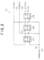
- FIG. 2 shows an example of a detailed circuit configuration of the clock generator 17 including a frequency divider.
- the three D-FFs 177, 178 and 179 have a CLK terminal connected to the clock input terminal 174.
- the CLK terminal of the D-FF 179 is a negated input terminal to which the oscillation frequency clock VCOCLK of the VCO 16 supplied from the VCO 16 through the clock input terminal 174 is supplied with a negated polarity.
- the D input terminal of the D-FF 177 of the first stage is connected to the Q output terminal of the second stage.
- the Q output terminal of the D-FF 177 of the first stage is connected to the QCLK output terminal 172 and also to the D input terminal of the D-FF 178 of the second stage.
- the D input terminal of the D-FF 178 of the second stage is a negated input terminal to which the Q output signal of the D-FF 177 of the first stage is inputted with a negated polarity.
- the Q output terminal of the D-FF 178 of the second stage is connected to the ICLK output terminal 171 and also to the D input terminal of the D-FF 179 of the third stage.
- the Q output terminal of the D-FF 179 of the third stage is connected to the I'CLK output terminal 173.
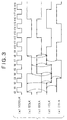
- waveforms (a) to (e) in the timing chart of FIG. 3 indicate waveforms at nodes (a) to (e) of FIG. 2, respectively. It is assumed that each of the D-FFs 177, 178 and 179 fetches the D input waveform thereof at the timing of a rising edge of the clock CLK thereto.
- the Q output signal (d) of the D-FF 178 has the "H" level before time t0, then since the D-FF 177 fetches the "H” level at time t0, the level of the Q output signal (b) thereof changes to the "H” level. Consequently, the level of the D input signal (c) of the D-FF 178 which is a reversed signal with respect to the Q output signal (b) of the D-FF 177 changes to the "L” level, and since the D-FF 178 fetches the "H” level immediately before the change to the "L” level, the Q output signal (d) of the D-FF 178 maintains the "H" level.
- the level of the Q output signal (e) of the D-FF 179 remains in the "H" level.
- the Q output signal (d) of the "L” level of the D-FF 178 is supplied to the D input terminal of the D-FF 177 and the D-FF 177 fetches the "L” level. Consequently, the level of the Q output signal (b) of the D-FF 177 changes to the "L” level.
- the Q output signal (b) of the "L” level is reversed and inputted as the D input to the D-FF 178. However, since the D-FF 178 fetches the "L” level immediately before the reversal, the Q output signal (d) of the D-FF 178 maintains the "L” level.
- the Q output signal (d) of the "L” level of the D-FF 178 is supplied to the D input terminal of the D-FF 177. Therefore, the Q output signal (b) of the D-FF 177 maintains the "L” level. Since the "H” level is supplied to the negated D input terminal of the D-FF 178 at this time and the D-FF 178 fetches the "H” level, the level of the Q output signal (d) of the D-FF 178 changes to the "H" level.
- the Q output signal (d) of the "H” level of the D-FF 178 is inputted as the D input to the D-FF 179 and fetched by the D-FF 179, and consequently, the level of the Q output signal (e) of the D-FF 179 changes to the "H” level.
- the Q output signal (d) of the "H” level of the D-FF 178 is supplied to the D input terminal of the D-FF 177 and fetched by the D-FF 177, and consequently, the level of the Q output signal (b) of the D-FF 177 changes to the "H” level.
- the negated D input of the D-FF 178 changes to the "L” level.
- the Q output signal (d) of the D-FF 178 maintains the "H" level.
- the clock signal extracted from the Q output terminal of the D-FF 178 is used as the clock signal ICLK and the clock signal extracted from the Q output terminal of the D-FF 179 is used as the clock signal I'CLK in this manner, since the CLK terminal of the D-FF 179 is formed as a negated input terminal, the clock signal I'CLK has a phase delayed by 45 degrees from that of the clock signal ICLK. Further, where the clock signal extracted from the Q output terminal of the D-FF 177 is used as the clock signal QCLK, the clock signal QCLK has a phase delayed by 90 degrees from that of the clock signal ICLK.
- the clock signal I'CLK generated by the clock generator 17 is supplied to the phase detection circuit 11 of FIG. 1 and used as a signal for detecting the phase, and the clock signals ICLK and QCLK are supplied to the frequency detection circuit 12 of FIG. 1 and used as reference signals for detecting the frequency.
- an NRZ digital signal is supplied to one of the input terminals of the phase detection circuit 11 and the data input terminal 121 of the frequency detection circuit 12 through the circuit input terminal 18. Meanwhile, the clock signal I'CLK generated by the clock generator 17 is supplied to the other input terminal of the phase detection circuit 11 while the clock signals ICLK and QCLK generated by the clock generator 17 are supplied to the ICLK input terminal 122 and the QCLK input terminal 123 of the frequency detection circuit 12, respectively.
- the frequency detection circuit 12 includes two D-FFs 124 and 125 and a control logic circuit 126.
- the D-FF 124 is connected at the D input terminal thereof to the ICLK input terminal 122 and at the CLK terminal thereof to the data input terminal 121.
- the D-FF 125 is connected at the D input terminal thereof to the QCLK input terminal 123 and at the CLK terminal thereof to the data input terminal 121.
- the timing waveform of the clock signal ICLK supplied to the ICLK input terminal 122 exhibits the "H” level within the period from time t0 to time t2, the "L” level within the period from time t2 to time t4, the "H” level within the period from time t4 to time t6, the “L” level within the period from time t6 to time t8, the "H” level within the period from time t8 to time t10, the “L” level within the period from time t10 to time t12, and the "H” level within the period from time t12 to time t14.
- the clock signal QCLK supplied to the QCLK input terminal 123 has a waveform having a phase delayed by 90 degrees from that of the clock signal ICLK and exhibits the "H” level within the period from time t1 to time t3, the “L” level within the period from time t3 to time t5, the "H” level within the period from time t5 to time t7, the “L” level within the period from time t7 to time t9, the "H” level within the period from time t9 to time t11, the “L” level within the period from time t11 to time t13, and the "H” level within the period from time t13 to time t15.
- the waveform of the input signal DATA supplied to the data input terminal 121 has the "L” level from time t0 to time t2, the "H” level from time t2 to time t6, the “L” level from time t6 to time t10, the “H” level from time t10 to time t13, and the "L” level later than time t13.
- the frequency detection circuit 12 has a function of opening a window when particular values (0, 1) are sampled from the data inputted to the D input terminals of the D-FFs 124 and 125 and outputting a result of comparison depending upon next sample values.
- the control logic circuit 126 of the next stage discriminates that the frequencies compared coincide with each other, and outputs nothing.
- next fetching timing falls between times t9 and t10 after the values (0, 1) are fetched, then the fetched values (samples) of the data now are (1, 1).
- the control logic circuit 126 of the next stage discriminates that the frequency of the clocks is lower than the frequency of the input signal DATA and outputs an UP pulse signal for raising the frequency.
- the control logic circuit 126 discriminates that the frequency of the clock is higher and outputs a DOWN pulse signal for lowering the frequency.
- the digital signal (pulse signal) of the UP/DOWN pulse signal obtained by frequency detection by the frequency detection circuit 12 in this manner is supplied to the charge pump circuit 14 of the next stage to turn the transistor of the charge pump circuit 14 on/off to cause electric current to flow out from/into the charge pump circuit 14.
- the charge pump circuit 14 for controlling the current is formed from, for example, a MOS transistor or a bipolar transistor.
- the output current of the charge pump circuit 14 is rectified into a dc voltage (dc signal) by the loop filter 15.
- the dc voltage is supplied as a control voltage to the VCO 16.
- the VCO 16 is configured such that, for example, it includes a variable capacitor, and the control voltage is applied to the variable capacitor.
- the variable capacitor varies its capacitance depending upon the control voltage applied thereto to control the frequency of the oscillation frequency clock of the VCO 16.
- the oscillation frequency clock is fed back to the frequency detection circuit 12 through the clock generator 17.
- the frequency detection circuit 12 compares the frequency of the clock signals ICLK and QCLK thus fed back and the NRZ digital signal DATA with each other. Since the frequency control operation by frequency comparison described above is repeated to lock the frequency of the oscillation frequency clock of the VCO 16 to a target frequency of the input signal DATA. In this locked state, the output voltage of the loop filter 15 is fixed and does not thereafter vary unless the frequency varies.
- operation of the frequency detection circuit 12 After the frequency of the oscillation frequency clock of the VCO 16 is locked to the target frequency of the input signal DATA, operation of the frequency detection circuit 12 remains in a fixed state (in particular, in a state wherein the UP/DOWN signal whose level is the output signal of the frequency detection circuit 12 is fixed to the "L" level). In this instance, if it is assumed that the current with which the capacitor C11 of the charge pump circuit 14 is charged/discharged is sufficiently high when compared with that of the charge pump circuit 13, then the phase detection circuit 11 substantially operates next to the operation of the frequency detection circuit 12.
- the de voltage based on the detection output of the phase detection circuit 11 is superposed on the de voltage based on the detection output of the frequency detection circuit 12 by the loop filter 15 to further vary the control voltage to be applied to the VCO 16 thereby to control the phase of the oscillation frequency clock of the VCO 16.
- the phase detection circuit 11 detects a delay/lead in phase of the clock signal I'CLK and hence of the oscillation frequency clock of the VCO 16 with respect to the input signal DATA.
- the output digital (pulse) signal of the phase detection circuit 11 is supplied in response to the delay/lead in phase to the charge pump circuit 13 of the next stage to control on/off of the transistor of the charge pump circuit 13 to cause, for example, electric current to flow out from/into the transistor.
- the charge pump circuit 13 for controlling the electric current is formed from, for example, a MOS transistor or a bipolar transistor similarly to the charge pump circuit 14 of the frequency detection circuit 12 side.
- the output current of the charge pump circuit 13 is rectified into a dc voltage by the loop filter 15.
- the dc voltage is superposed on the dc voltage of the frequency detection circuit 12 side by the loop filter 15 and supplied as a control voltage to the VCO 16 so that it is applied to the variable capacitor mentioned hereinabove.
- the variable capacitor changes its capacitance in response to the control voltage applied thereto to control the phase of the oscillation frequency clock of the VCO 16.
- the oscillation frequency clock of the VCO 16 having the controlled phase is fed back as the clock signal I'CLK to the phase detection circuit 11 through the clock generator 17.
- the phase detection circuit 11 compares the phases of the fed back clock signal I'CLK and the NRZ digital signal DATA with each other. Then, the operations of phase detection and phase control described above are repeated until also the phase of the oscillation frequency clock of the VCO 16 coincides with the phase of the input signal DATA finally.
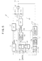
- the PLL circuit 10 described above uses the charge pump circuits 13 and 14 of a single output configuration and the VCO 16 of a single input configuration and further uses the loop filter 15 which includes the resistor R11 connected between the output terminals of the charge pump circuits 13 and 14 and the capacitor C11 connected between the output terminal of the charge pump circuit 14 and the ground, the PLL circuit is not necessarily limited to the specific PLL circuit having the configuration described.
- the PLL circuit may otherwise be, for example, such a PLL circuit 10' as shown in FIG. 5 which uses charge pump circuits 13' and 14' of a differential output configuration and a VCO 16' of a differential input configuration and besides uses a loop filter 20 which includes a resistor R12 connected between ones of output terminals of the charge pump circuits 13' and 14', a capacitor C12 connected between the differential output terminals of the charge pump circuit 14' and another resistor R13 connected between the other output terminals of the charge pump circuit 14' and 13'.
- a loop filter 20 which includes a resistor R12 connected between ones of output terminals of the charge pump circuits 13' and 14', a capacitor C12 connected between the differential output terminals of the charge pump circuit 14' and another resistor R13 connected between the other output terminals of the charge pump circuit 14' and 13'.
- FIG. 6 shows an example of a detailed circuit configuration of the frequency detection circuit 12 used in the PLL circuit 10 (10') to which the present invention is applied, particularly an example of an internal configuration of the control logic circuit 126 of the frequency detection circuit 12 described hereinabove.
- the clock signal ICLK is supplied to an ICLK input terminal 31, and the clock signal QCLK is supplied to a QCLK input terminal 32. Meanwhile, an NRZ digital signal DATA is supplied to a data input terminal 33.
- the ICLK input terminal 31, QCLK input terminal 32 and data input terminal 33 correspond to the ICLK input terminal 122, QCLK input terminal 123 and data input terminal 121 of FIG. 1, respectively.
- the ICLK input terminal 31 is connected to the D input terminal of a D-FF 34, and the QCLK input terminal 32 is connected to the D input terminal of another D-FF 35.
- the data input terminal 33 is connected to the CLK terminals of the D-FFs 34 and 35.
- the D-FFs 34 and 35 correspond to the D-FFs 124 and 125 of FIG. 1, respectively.
- Each of the D-FFs 34 and 35 is configured such that it fetches D input data thereto at a rising edge of a clock CLK thereto.
- the D-FF 34 has a function of sampling the clock signal ICLK at a rising edge of the input signal DATA
- the D-FF 35 has a function of sampling the clock signal QCLK at a rising edge of the input signal DATA.
- the Q output terminal of the D-FF 34 is connected to an input terminal A of a 2-input OR gate 36 and connected also to a negated input terminal A of a 3-input OR gate 38 and further to an input terminal B of a 3-input OR gate 39.
- the Q output terminal of the D-FF 35 is connected to a negated input terminal B of the OR gate 36, to a negated input terminal B of the OR gate 38 and to an input terminal C of the OR gate 39.
- the output terminal of the OR gate 36 is connected to the D input terminal of a D-FF 37.
- the CLK input terminal of the D-FF 37 is connected to the ICLK input terminal 31.
- the Q output terminal of the D-FF 37 is connected to an input terminal C of the OR gate 38 and also to an input terminal A of the OR gate 39.
- the output terminals of the OR gates 38 and 39 are connected to the D input terminals of D-FFs 40 and 41, respectively.
- the CLK input terminals of the D-FFs 40 and 41 are connected to the ICLK input terminal 31.
- the Q output terminals of the D-FFs 40 and 41 are connected to circuit output terminals 42 and 43, respectively. It is to be noted that the Q output terminals of the D-FFs 40 and 41 are formed as negated output terminals.
- the OR gate 36, D-FF 37, OR gates 38 and 39 and D-FFs 40 and 41 described above cooperatively form the control logic circuit 126 of FIG. 1. It is to be noted that the circuit configuration of FIG. 6 is a mere example, and the control logic circuit 126 may have some other circuit configuration.
- FIG. 7 illustrates a timing chart when the UP pulse signal is outputted
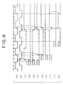
- FIG. 8 illustrates a timing chart when the DOWN pulse signal is outputted.
- waveforms (a) to (k) indicate waveforms at nodes (a) to (k) of FIG. 6, respectively.
- the D-FFs 34 and 35 fetch the clock signals ICLK (a) and QCLK (b) at a rising edge of the waveform of the input signal DATA (c).
- the clock signal ICLK (a) has the "L” level
- the clock signal QCLK (b) has the "H” level
- the D-FFs 34 and 35 fetch the "L” and "H” levels, respectively. Consequently, the level of the Q output signal (d) of the D-FF 34 changes to the "L” level and the level of the Q output signal (e) of the D-FF 35 changes to the "H” level.
- the next rising edge of the waveform of the input signal DATA (c) supplied to the CLK terminals of the D-FFs 34 and 35 is included in the period between times t9 and t10, and the levels of the clock signal ICLK (a) and the clock signal QCLK (b) at the point of time are the "H” level. Accordingly, the level of the Q output signal (d) of the D-FF 34 changes from the "L” level to the "H” level within the period between the times t9 and t10.
- the Q output signal (e) of the D-FF 35 does not change but remains at the "H” level. Thereafter, the waveform of the input signal DATA (c) does not exhibit a change till time t16 and the waveform does not include a rising edge. Therefore, the Q output signals (d) and (e) of the D-FFs 34 and 35 do not change but maintain the levels thereof as they are.
- the "L" level of the Q output signal (d) of the D-FF 34 is supplied to the input terminal A of the OR gate 36 while the "H” level of the Q output signal (e) of the D-FF 35 is supplied to the negated input terminal B of the OR gate 36, and therefore, the level of the output signal (f) of the OR gate 36 changes to the "L” level. Further, the next change from the "L” level to the "H” level of the input signal DATA (c) appears within the period between times t9 and t10.
- the Q output signal (d) of the D-FF 34 changes from the “L” level to the “H” level while the level of the Q output signal (e) of the D-FF 35 remains at the “H” level. Therefore, the level of the output signal (f) of the OR gate 36 changes from the “L” level to the "H” level. Thereafter, since the waveform of the input signal DATA (c) does not have a change till time t16, the output signal (f) of the OR gate 36 maintains the "H" level.
- the output signal (f) of the OR gate 36 is supplied to the D input terminal of the D-FF 37.
- the clock signal ICLK (a) different from the clock signal supplied to the D-FFs 34 and 35 is supplied as the CLK input to the D-FF 37. Consequently, the D-FF 37 fetches the output signal (f) of the OR gate 36, which is the D input thereto, at a rising edge of the clock signal ICLK (a).
- the D-FF 37 fetches the output signal (f) of the OR gate 36 at the rising timing t4 of the clock signal ICLK (a), and thereupon, the level of the output signal (g) thereof changes to the "L” level. Then, at the next rising timing t8 of the clock signal ICLK (a), since the Q output signal (f) of the OR gate 36 has the "L” level, the output signal (g) of the D-FF 37 does not change but maintains the "L” level.
- the level of the Q output signal (g) of the D-FF 37 changes from the “L” level to the "H” level.
- the Q output signal (g) of the D-FF 37 has the "H” level, and consequently, also after time t16, the Q output signal (g) keeps the state of the "H” level.
- the 3-input OR gate 38 receives, at the negated input terminal A thereof, the Q output signal (d) of the D-FF 34, at the negated input terminal B thereof, the Q output signal (e) of the D-FF 35, and at the input terminal C thereof, the Q output signal (g) of the D-FF 37.
- the inverted signal of the Q output signal (d) of the D-FF 34 exhibits the "H” level after a DATA rising edge between times t2 and t3 till another DATA rising edge between times t9 and t10 and exhibits the "L” level after the timing of the DATA rising edge
- the inverted signal of the Q output signal (e) of the D-FF 35 exhibits the "L” level after time t4 till time t12 and exhibits the "H” level after time t12.
- the output signal (h) of the OR gate 38 exhibits the "H” level after time t4 till the DATA rising edge between times t9 and t10 and exhibits the "L” level after the point of time of the DATA rising edge till time t12, and then exhibits the "H” level after time t12.
- the 3-input OR gate 39 receives, at the input terminal A thereof, the Q output signal (g) of the D-FF 37, at the input terminal B thereof, the Q output signal (d) of the D-FF 34, and at the input terminal C thereof, the Q output signal (e) of the D-FF 35.
- the Q output signal (d) of the D-FF 34 exhibits the "L” level after the DATA rising edge between times t2 and t3 till the DATA rising edge between times t9 and t10 and exhibits the "H” level after the timing of the DATA rising edge.
- the Q output signal (e) of the D-FF 35 exhibits the "H” level after the DATA rising edge between times t2 and t3.
- the Q output signal (g) of the D-FF 37 exhibits the "L” level after time t4 till time t12 and exhibits the "H” level after time t12. Accordingly, the output signal (i) of the OR gate 39 maintains the "H" level after time t4.
- the output signal (h) of the OR gate 38 is supplied to the D input terminal of the D-FF 40.
- the D-FF 40 fetches the output signal (h) of the OR gate 38, which is D input data thereto, in synchronism with the clock signal ICLK (a).
- the D-FF 40 fetches the "H" level of the output signal (h) at the rising edge of the clock signal ICLK (a) at time t8.
- the level of the inverted Q output signal (j) of the D-FF 40 changes to the "L” level.
- the next rising edge of the clock signal ICLK (a) appears at time t12. Since the output signal (h) of the OR gate 38 at time t12 has the “L” level, the level of the inverted Q output signal (j) of the D-FF 40 changes to the "H” level. Further, since the next rising edge of the clock signal ICLK (a) appears at time t16 and the output signal (h) of the OR gate 38 then has the "H” level, the level of the inverted Q output signal (j) of the D-FF 40 changes from the "H” level to the "L” level.
- the inverted Q output signal (j) of the D-FF 40 is used as the UP pulse signal and supplied from the circuit output terminal 42 to the charge pump circuit (charge pump circuit 14 in FIG. 1) of the next stage.
- the output signal (i) of the OR gate 39 is supplied to the D input terminal of the D-FF 41. Since the clock signal ICLK (a) is supplied also as the D input to the D-FF 41, the D-FF 41 fetches the D input data at the same fetching timing as that of the D-FF 40. In particular, since the output signal (i) of the OR gate 39 has the "H" level at time t8, the inverted Q output signal (k) of the D-FF 41 has the "L" level.
- the inverted Q output signal (k) of the D-FF 41 similarly continues to output the "L” level.
- the inverted Q output signal (k) of the D-FF 41 is used as the DOWN pulse signal and supplied from the circuit output terminal 43 to the charge pump circuit (charge pump circuit 14 of FIG. 1) of the next stage.
- the D-FFs 34 and 35 fetch D input data, that is, the clock signals ICLK (a) and QCLK (b), at a rising edge of the waveform of the input signal DATA (c).
- the clock signal ICLK (a) has the "L” level
- the clock signal QCLK (b) has the "H” level
- the D-FFs 34 and 35 fetch the "L” and "H” levels, respectively. Consequently, the level of the Q output signal (d) of the D-FF 34 changes to the "L” level and the level of the Q output signal (e) of the D-FF 35 changes to the "H” level.
- the next rising edge of the waveform of the input signal DATA (c) supplied to the CLK terminals of the D-FFs 34 and 35 is included in the period between times t11 and t12, and the levels of the clock signal ICLK (a) and the clock signal QCLK (b) at the point of time are the "L” level. Accordingly, the level of the Q output signal (d) of the D-FF 34 maintains the "L” level.
- the level of the clock signal QCLK (b) is the "L” level
- the level of the Q output signal (e) of the D-FF 35 changes from the "H” level to the "L” level.
- the waveform of the input signal DATA (c) does not exhibit a change and the waveform thereof does not include a rising edge. Therefore, the Q output signals (d) and (e) of the D-FFs 34 and 35 do not change but maintain the levels thereof.
- the "L" level of the Q output signal (d) of the D-FF 34 is supplied to the input terminal A of the OR gate 36 while the "L” level of the Q output signal (e) of the D-FF 35 is supplied to the negated input terminal B of the OR gate 36, and therefore, the level of the output signal (f) of the OR gate 36 changes to the "L” level. Further, the next variation from the "L” level to the "H” level of the input signal DATA (c) at the next changing point appears within the period between times t11 and t12.
- the Q output signal (d) of the D-FF 34 remains at the “L” level while the level of the Q output signal (e) of the D-FF 35 changes from the "H” level to the “L” level. Therefore, the level of the output signal (f) of the OR gate 36 changes from the “L” level to the "H” level. Thereafter, since the waveform of the input signal DATA (c) does not have a change, the output signal (f) of the OR gate 36 maintains the "H" level.
- the output signal (f) of the OR gate 36 is supplied to the D input terminal of the D-FF 37.
- the clock signal ICLK (a) different from the input signal DATA supplied to the CLK input terminals of the D-FFs 34 and 35 is supplied as the CLK input to the D-FF 37. Consequently, the D-FF 37 fetches the output signal (f) of the OR gate 36, which is the D input thereto, at a rising edge of the clock signal ICLK (a).
- the D-FF 37 fetches the output signal (f) of the OR gate 36 at the rising timing t4 of the clock signal ICLK (a), and thereupon, the level of the Q output signal (g) thereof changes to the "L” level. Then, at the next rising timing t8 of the clock signal ICLK (a), since the output signal (f) of the OR gate 36 has the "L” level, the Q output signal (g) of the D-FF 37 does not change but maintains the "L” level.
- the level of the Q output signal (g) of the D-FF 37 changes from the “L” level to the "H” level.
- the Q output signal (g) of the D-FF 37 has the "H” level, and consequently, also after time t16, the Q output signal (g) keeps the state of the "H” level.
- the 3-input OR gate 38 receives, at the negated input terminal A thereof, the Q output signal (d) of the D-FF 34, at the negated input terminal B thereof, the Q output signal (e) of the D-FF 35, and at the input terminal C thereof, the Q output signal (g) of the D-FF 37.
- the inverted signal of the Q output signal (d) of the D-FF 34 exhibits the "H” level after a DATA rising edge between times t2 and t3 till time 18, and the inverted signal of the Q output signal (e) of the D-FF 35 exhibits the "L” level after the DATA rising edge between times t2 and t3 till a time between times t11 and t12 and exhibits the "H” level after the time between times t11 and t12.
- the Q output signal (g) of the D-FF 37 has the "L” level from time t4 to time t12 and exhibits the "H” level after time t12. Accordingly, the output signal (h) of the OR gate 38 exhibits the "H" level after time t4.
- the 3-input OR gate 39 receives, at the input terminal A thereof, the Q output signal (g) of the D-FF 37, at the input terminal B thereof, the Q output signal (d) of the D-FF 34, and at the input terminal C thereof, the Q output signal (e) of the D-FF 35.
- the Q output signal (d) of the D-FF 34 exhibits the "L” level after the DATA rising edge between times t2 and t3.
- the Q output signal (e) of the D-FF 35 exhibits the "H” level after the DATA rising edge between times t2 and t3 till the DATA rising edge of the waveform of the input signal DATA between times t11 and t12 and exhibits the "L” level after the timing of the rising edge.
- the Q output signal (g) of the D-FF 37 exhibits the "L” level after time t4 till time t12 and exhibits the "H” level after time t12.
- the output signal (i) of the OR gate 39 exhibits the "H” level after time t4 till the rising edge of the input signal DATA between times t11 and t12, and exhibits the "L” level after the DATA rising edge till time t12. Further, the output signal (i) of the OR gate 39 maintains the "H” level within the period after time t12.
- the output signal (h) of the OR gate 38 is supplied to the D input terminal of the D-FF 40.
- the D-FF 40 fetches the output signal (h) of the OR gate 38, which is D input data thereto, in synchronism with the clock signal ICLK (a).
- the D-FF 40 fetches the "H" level of the output signal (h) of the OR gate 38 at the rising edge of the clock signal ICLK (a) at time t8.
- the level of the inverted Q output signal (j) of the D-FF 40 changes to the "L” level.
- the next rising edge of the clock signal ICLK (a) appears at time t12 and at time t16. Since the output signal (h) of the OR gate 38 at time t12 and time t16 has the "H” level, the inverted Q output signal (j) of the D-FF 40 continues to have the "L” level.
- the output signal (i) of the OR gate 39 is supplied to the D input terminal of the D-FF 41. Since the clock signal ICLK (a) is supplied also as the D input to the D-FF 41, the D-FF 41 fetches the D input data at the same fetching timing as that of the D-FF 40. In particular, since the output signal (i) of the OR gate 39 has the "H" level at time t8, the inverted Q output signal (k) of the D-FF 41 has the "L" level.
- the level of the inverted Q output signal (k) of the D-FF 41 changes to the "H” level. Further, since the output signal (i) of the OR gate 39 at time 16 has the "H” level, the level of the inverted Q output signal (k) of the D-FF 41 changes from the "H” level to the "L” level.
- the inverted Q output signal (k) of the D-FF 41 is used as the DOWN pulse signal and supplied from the circuit output terminal 43 to the charge pump circuit (charge pump circuit 14 of FIG. 1) of the next stage.
- the UP pulse signal (j) which is the inverted Q output signal of the D-FF 40 continues to keep the "L” level within the period from time t8 to time 18
- the DOWN pulse signal (k) which is the inverted Q output signal of the D-FF 41 maintains the "H” level within the period from time t12 to time 16 to control the electric current to the charge pump circuit 14 of the next stage to generate the control voltage to the VCO 16.
- the frequency detection circuit 12 described above samples the "L” level (logic “0") of the clock signal ICLK and the “H” level (logic “1”) of the clock signal QCLK at a rising edge of the serial input signal DATA
- any combination of logic values may be used instead.
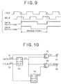
- the combination of logic values described above in connection with the frequency detection circuit 12 is adopted, as can be seen apparently from the timing chart of FIG. 9, the combination of logic values is positioned substantially at the center of one period of the input signal DATA. Consequently, since control upon phase adjustment after the frequency adjustment can be performed in the proximity of the center of one period of the input signal DATA, there is an advantage that a wide control range can be used for the phase control.
- the frequency detection circuit 12 described above samples the clock signal ICLK and the clock signal QCLK only at a rising edge of the input signal DATA, it is otherwise possible to sample the clock signal ICLK and the clock signal QCLK only at a falling edge of the input signal DATA. Also in this instance, a wrong control signal (UP pulse signal/DOWN pulse signal) is not generated at all similarly, and a stabilized PLL operation can be anticipated.
- phase detection circuit 11 used in the PLL circuit 10 (10') is described.
- An example of a circuit configuration of the phase detection circuit 11 is shown in FIG. 10. First, the circuit configuration of the phase detection circuit 11 is described.
- a data input terminal 51 to which the input signal DATA is supplied is connected to the D input terminal of a D-FF 53 and also to an input terminal A of a 2-input exclusive OR (EX-OR) gate 55.
- a CLK input terminal 52 to which the clock signal I'CLK generated by the clock generator 17 is supplied is connected to the CLK terminal of the D-FF 53 and also to the negated CLK terminal of a D-FF 54.
- the Q output terminal of the D-FF 53 is connected to the other input terminal B of the EX-OR gate 55, an input terminal A of a 2-input EX-OR gate 56 and the D input terminal of the D-FF 54.
- the Q output terminal of the D-FF 54 is connected to the other input terminal B of the EX-OR gate 56.
- the output terminal of the EX-OR gate 55 is connected to an UP output terminal 57 while the output terminal of the EX-OR gate 56 is connected to a DOWN output terminal 58.
- phase detection circuit 11 having the configuration described above is described with reference to a timing chart of FIG. 11. It is to be noted that, in the timing chart of FIG. 11, waveforms (a) to (f) indicate waveforms at nodes (a) to (f) of FIG. 10, respectively.
- the waveform of the input signal DATA (b) falls within the period between times t1 and t2 and thereafter maintains the "L” level until it rises within the period between times t5 and t6; maintains the "H” level until it falls within the period between times t8 and t9; maintains the "L” level until it rises within the period between times t10 and t11; maintains the "H” level until it falls within the period between times t12 and t13; and thereafter maintains the "L” level till time t15.
- the D-FF 53 fetches the "L” level of the input signal DATA (b) at the rising timing t2 of the clock signal I'CLK (a). Consequently, the level of the Q output signal (c) of the D-FF 53 changes to the "L” level. At the next rising timing t4 of the clock signal I'CLK (a), since the input signal DATA does not change but maintains the "L” level, also the Q output signal (c) of the D-FF 53 does not change but maintains the "L” level.
- the level of the Q output signal (c) of the D-FF 53 changes to the "H” level. Further, at the rising timing of the clock signal I'CLK (a) at time t8, since the input signal DATA has the "H” level and the D-FF 53 fetches the "H” level, the level of the Q output signal (c) of the D-FF 53 does not change but remains at the "H” level.
- the Q output signal (c) of the D-FF 53 changes from the "H” level to the "L” level.
- the level of the Q output signal (c) of the D-FF 53 changes to the "H” level, and then at the next rising timing t14 of the clock signal I'CLK (a), the input signal DATA has the "L” level. Consequently, the D-FF 53 fetches the "L” level of the input signal DATA, and the Q output signal (c) thereof changes to the "L” level.
- an inverted clock of the clock signal I'CLK (a) is supplied as the CLK input to the D-FF 54. Accordingly, the D-FF 54 fetches the input signal DATA at times t1, t3, t5, t7, t9, t11, t13 and t15 at which the clock signal I'CLK (a) falls.
- the Q output signal (c) of the D-FF 53 has the "H” level, and therefore, the level of the Q output signal (d) of the D-FF 54 changes to the "H” level and remains at the “H” level till the next falling timing t3 of the clock signal I'CLK (a).
- the D-FF 54 fetches the "L” level, and consequently, the level of the Q output signal (d) thereof changes from the "H” level to the "L” level. Then, the Q output signal (d) maintains the "L” level till immediately before time t7 past time t5.
- the level of the Q output signal (d) of the D-FF 54 changes to the "H” level because the D-FF 54 fetches the "H” level of the Q output signal (c).
- the Q output signal (c) of the D-FF 53 does not change, but at time t10, the level of the Q output signal (c) changes to the "L” level and thereafter remains at the "L” level till time t12.
- the Q output signal (c) of the D-FF 53 has the "L” level, and since the D-FF 54 fetches the "L” level, the level of the Q output signal (d) thereof changes from the "H” level to the "L” level.
- the D-FF 54 fetches the "H” level and the level of the Q output signal (d) thereof changes from the “L” level to the "H” level.
- the "H” level is kept till the next falling timing t15 of the clock signal I'CLK (a), and at time t15, the "L” level of the Q output signal (c) of the D-FF 53 is fetched into the D-FF 54. Consequently, the level of the Q output signal (d) of the D-FF 54 changes from the "H” level to the "L” level.
- the logic values of the input signal DATA (b) and the Q output signal (c) of the D-FF 53 are different from each other within the period after a point of time at which the level of the input signal DATA (b) changes from the "H” level to the "L” level between times t1 and t2 till time t2 at which the Q output signal (c) of the D-FF 53 exhibits the "H” level, the period after a point of time at which the level of the input signal DATA (b) changes from the "L” level to the "H” level between times t5 and t6 till time t6 at which the level of the Q output signal (c) of the D-FF 53 changes from the "L” level to the "H” level, the period after a point of time at which the level of the input signal DATA (b) changes from the "H” level to the "L” level between times t8 and t9 till time t10, the period after a point of time at which the level of the input signal DATA (b) changes
- the output signal (e) of the EX-OR gate 55 exhibits the "H” level.
- the output signal (e) of the EX-OR gate 55 has the "L” level.
- the output signal (e) of the EX-OR gate 55 is used as the UP pulse signal.
- the logical values of the Q output signal (c) of the D-FF 53 and the Q output signal (d) of the D-FF 54 are different from each other within the period from time t2 to time t3, the period from time t6 to time t7, the period from time t10 to time t11, the period from time t12 to time t13, and the period from time t14 to time t15.
- the output signal (f) of the EX-OR gate 56 exhibits the "H” level.
- the output signal (f) of the EX-OR gate 56 has the "L” level.
- the output signal (f) of the EX-OR gate 56 is used as the DOWN pulse signal.
- each of the pulse waveforms of the UP pulse signal (e) and the DOWN pulse signal (f) is generated once.
- the pulse width of the DOWN pulse signal (f) is always fixed, and phase control is performed by adjusting the pulse width of the UP pulse signal (e).
- the phase detection circuit 11 begins to operate during operation of the frequency detection circuit 12, and the point of time of a rising edge at which the level of the clock signal I'CLK varies from the "L" level to the "H” level is synchronized particularly with the center of the width of a pulse (waveform) of the input signal DATA by the operation of the phase detection circuit 11 described above.
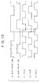
- phase synchronism is described with reference to a timing chart of FIG. 12.
- the waveform (a) indicates the input signal DATA when the duty ratio is high; the waveform (b) indicates the input signal DATA when the duty ratio is low; the waveform D (c) indicates the clock signal I'CLK; the waveform (d) indicates the clock signal ICLK; and the waveform (e) indicates the clock signal QCLK.
- the point of time of a rising edge of the clock signal I'CLK (c) is positioned at the center of the waveform (width) of the input signal DATA (a) where the duty ratio is high, and is synchronized also with the center of the waveform (width) of the input signal DATA (b) where the duty ratio is low.
- the point of time of a rising edge of the clock signal I'CLK is positioned at the center of the period (pulse width) of the "H" level of the input signal DATA.
- the phase detection circuit samples the clock signals ICLK and QCLK at a changing point of the input signal DATA
- the sample value of the clock signal ICLK by the frequency detection circuit with respect to a variation of the duty ratio of the input signal DATA in a locked state is unstable.
- the clock signal I'CLK having a predetermined phase for example, a phase delayed by 45 degrees
- the clock signal ICLK is produced based on the oscillation frequency clock VCOCLK of the VCO 16 and the point of time of a rising edge of the clock signal I'CLK is positioned at the center of the eye pattern of the input signal DATA in a phase-locked state by the phase detection circuit 11 as described above
- the withstanding property of the phase control against the duty distortion can be improved as described below.
- the width of variation of the duty ratio within which the sample values of (0, 1) are maintained is greater than that in the related art wherein a portion of the clock signal ICLK in the proximity of a falling edge is sampled at a changing point of the input signal DATA as illustrated in FIG. 21.
- the width of variation of the duty ratio within which the sample values when the frequency detection circuit 12 samples the clock signals ICLK and QCLK in synchronism with the input signal DATA are fixed is increased.
- the frequency detection circuit 12 samples the clock signals ICLK and QCLK only at a rising edge (or a falling edge) of the serial input signal DATA, even if the duty ratio of the input signal DATA varies, if the frequencies of the input signal DATA and the clock signals ICLK and QCLK coincide with each other, sets of sample values of the clock signal ICLK and the clock signal QCLK are always equal to each other. Consequently, the frequency detection circuit 12 does not generate a wrong control signal (UP pulse signal/DOWN pulse signal) at all and can achieve a stabilized PLL operation.
- UP pulse signal/DOWN pulse signal UP pulse signal/DOWN pulse signal
- the clock generator 17 produces the clock signal I'CLK having a particular phase, for example, having a phase delayed by 45 degrees, with respect to the clock signal ICLK based on the oscillation frequency clock VCOCLK of the VCO 16 and inputs the clock signal I'CLK together with the input signal DATA to the phase detection circuit 11, the phase detection circuit 11 sets the rising timing of the clock signal I'CLK to the center of the pulse width (for example, the "H" level period) of the input signal DATA.
- the PLL circuit described above which uses the frequency detection circuit 12 configured so as to sample the clock signals ICLK and QCLK at only either rising or falling edges of the input signal DATA is configured such that the clock signal I'CLK having a phase, for example, delayed by 45 degrees with respect to the clock signal ICLK is inputted together with the input signal DATA to the phase detection circuit 11.
- the PLL circuit is not limited to the specific PLL circuit described, but the present invention can be applied also to a PLL circuit which uses a conventional frequency detection circuit configured so as to sample the clock signals ICLK and QCLK at both of rising and falling edges of the input signal DATA.
- FIG. 13 is a block diagram showing an example of a configuration of an optical communication reception apparatus to which the present invention is applied.
- an optical signal is received and converted into an electric signal by a photo-detector (PD) 61 and is extracted as signal current from the photo-detector 61.
- the signal current is converted into a signal voltage by an I (current) to V (voltage) conversion circuit 62, amplified by an amplifier 63 and supplied to a retiming circuit 64 and a PLL circuit 65.
- the PLL circuit 65 extracts, from the received data supplied thereto from the amplifier 63, a clock component included in the received data and produces and supplies a new clock signal having a phase synchronized with the clock component to the retiming circuit 64.
- the PLL circuit 10 (10') described hereinabove can be used for the PLL circuit 65.
- the retiming circuit 64 retimes (a kind of waveform shaping) the received data supplied thereto from the amplifier 63 based on the clock signal supplied thereto from the PLL circuit 65 and outputs the retimed received data.
- the PLL circuit to which the present invention is applied is used as the PLL circuit 65 of the reception apparatus for use with optical communication in which, for example, NRZ digital data are used in this manner, even if the duty ratio of the input signal to the PLL circuit varies, the convergence time required for frequency detection of the frequency detection circuit is short and a malfunction of the frequency detection circuit with a control signal is less likely to occur and consequently a stabilized PLL operation can be achieved. Consequently, the PLL circuit 65 does not malfunction with data of a transmission signal which is liable to suffer from duty distortion, and accordingly, the retiming processing by the retiming circuit 64 can be performed with a higher degree of certainty.
- the present invention is applied to a reception apparatus for optical communication
- the application of the present invention is not limited to this, but the present invention can be applied particularly to processing systems which process data which are liable to suffer from duty distortion.
Landscapes
- Engineering & Computer Science (AREA)
- Power Engineering (AREA)
- Stabilization Of Oscillater, Synchronisation, Frequency Synthesizers (AREA)
- Synchronisation In Digital Transmission Systems (AREA)
- Optical Communication System (AREA)
Abstract
Description
Claims (24)
- A PLL circuit (10), comprising:an oscillator (16) for generating an oscillation frequency signal having a variable oscillation frequency;a signal generation circuit (17) for generating, based on the oscillation frequency signal of said oscillator, a first signal (ICLK) having a phase same as that of the oscillation frequency signal, a second signal (QCLK) having a fixed phase difference from the first signal, and a third signal (I'CLK) having a phase difference smaller than the phase difference between the first and second signals from the first signal;a phase detection circuit (11) for comparing the phases of the third signal generated by said signal generation circuit and an input signal and outputting, based on a result of the comparison, a first phase control signal for advancing the phase of the oscillation frequency signal of said oscillator or a second phase control signal for delaying the phase of the oscillation frequency signal of said oscillator; anda frequency detection circuit (12) for fetching the first and second signals generated by said signal generation circuit in synchronism with the input signal and outputting, based on the fetched signals, a first frequency control signal for raising the frequency of the oscillation frequency signal of said oscillator or a second frequency control signal for lowering the frequency of the oscillation frequency signal of said oscillator.
- A PLL circuit according to claim 1, wherein the first, second and third signals (ICLK, QCLK, I'CLK) are clock signals.
- A PLL circuit according to claim 2, wherein the phase of the second signal (QCLK) is delayed by 90 degrees from that of the first signal (ICLK).
- A PLL circuit according to claim 3, wherein the phase of the third signal (I'CLK) is delayed by more than 0 degree but smaller than 90 degrees from that of the first signal (ICLK).
- A PLL circuit according to claim 4, wherein the phase of the third signal (I'CLK) is delayed by 45 degrees from that of the first signal (ICLK).
- A PLL circuit according to claim 1, wherein said frequency detection circuit (12) fetches the first and second signals (ICLK, QCLK) in synchronism with the input signal for each period of the input signal, logically operates the currently fetched signals and the signals fetched in the preceding period and outputs, based on a result of the logical operation, the first frequency control signal for raising the frequency of the oscillation frequency signal of said oscillator (16) or the second frequency control signal for lowering the frequency of the oscillation frequency signal of said oscillator.
- A PLL circuit according to claim 6, wherein said frequency detection circuit (12) includes a first sampling circuit (124) for fetching the first signal in synchronism with the input signal for each period of the input signal, a second sampling circuit (125) for fetching the second signal in synchronism with the input signal for each period of the input signal, and a control logic circuit (126) for storing the signals fetched by said first and second sampling circuits, logically operating the stored signals and the signals fetched subsequently by said first and second sampling circuits and generating, based on a result of the logical operation, the first frequency control signal or the second frequency control signal.
- A PLL circuit according to claim 7, wherein said control logic circuit (126) includes a first logical operation circuit (36) for logically operating output signals of said first and second sampling circuits (124, 125), a first storage circuit (37) for storing an output signal of said first logical operation circuit, a second logical operation circuit (38) for logically operating the output signals of said first and second sampling circuits and the stored signal of said first storage circuit, a third logical operation circuit (39) for logically operating a signal obtained by logical processing of the output signals of said first and second sampling circuit and the stored signal of said first storage circuit, second storage means (40) for storing an output signal of said second logical operation circuit, and third storage means (41) for storing an output signal of said third logical operation circuit.
- A PLL circuit according to claim 7, wherein said first and second sampling circuits (124, 125) sample the first and second signals, respectively, at a timing of a rising edge or a falling edge of the input signal.
- A PLL circuit according to claim 7, wherein each of said first and second sampling circuits (124;125) includes a flip-flop circuit.
- A PLL circuit according to claim 10, wherein said flip-flop is a D-type flip-flop.
- A PLL circuit according to claim 11, wherein the D-type flip-flops fetch the first and second signals at a timing of a rising edge of a clock input thereto.
- A PLL circuit according to claim 8, wherein each of said first, second and third logical operation circuits (36, 38, 39) includes an OR circuit.
- A PLL circuit according to claim 8, wherein each of said first, second and third storage circuits (37, 40, 41) includes a flip-flop circuit.
- A PLL circuit according to claim 14, wherein said flip-flop circuit is a D-type flip-flop.
- An optical communication reception apparatus, comprising:light reception means (61, 62) for receiving an optical signal, converting the optical signal into an electric signal and outputting the electric signal;a PLL circuit (65) for producing a clock signal synchronized with the output signal of said light reception means; anda retiming circuit (64) for retiming the output signal of said light reception means based on the clock signal produced by said PLL circuit;said PLL circuit including an oscillator (16) for generating an oscillation frequency signal having a variable oscillation frequency, a signal generation circuit (17) for generating, based on the oscillation frequency signal of said oscillator, a first signal (ICLK) having a phase same as that of the oscillation frequency signal, a second signal (QCLK) having a fixed phase difference from the first signal, and a third signal (I'CLK) having a phase difference smaller than the phase difference between the first and second signals from the first signal, a phase detection circuit (11) for comparing the phases of the third signal generated by said signal generation circuit and an input signal and outputting, based on a result of the comparison, a first phase control signal for advancing the phase of the oscillation frequency signal of said oscillator or a second phase control signal for delaying the phase of the oscillation frequency signal of said oscillator, and a frequency detection circuit (12) for fetching the first and second signals generated by said signal generation circuit in synchronism with the input signal and outputting, based on the fetched signals, a first frequency control signal for raising the frequency of the oscillation frequency signal of said oscillator or a second frequency control signal for lowering the frequency of the oscillation frequency signal of said oscillator.
- An optical communication reception apparatus according to claim 16, wherein the first, second and third signals (ICLK, QCLK, I'CLK) are clock signals.
- An optical communication reception apparatus according to claim 17, wherein the phase of the second signal (QCLK) is delayed by 90 degrees from that of the first signal.
- An optical communication reception apparatus according to claim 18, wherein the phase of the third signal (I'CLK) is delayed by more than 0 degree but smaller than 90 degrees from that of the first signal (ICLK).
- An optical communication reception apparatus according to claim 19, wherein the phase of the third signal (I'CLK) is delayed by 45 degrees from that of the first signal (ICLK).
- An optical communication reception apparatus according to claim 16, wherein said frequency detection circuit (12) fetches the first and second signals (ICLK, QCLK) in synchronism with the input signal for each period of the input signal, logically operates the currently fetched signals and the signals fetched in the preceding period and outputs, based on a result of the logical operation, the first frequency control signal for raising the frequency of the oscillation frequency signal of said oscillator (16) or the second frequency control signal for lowering the frequency of the oscillation frequency signal of said oscillator.
- An optical communication reception apparatus according to claim 21, wherein said frequency detection circuit (12) includes a first sampling circuit (124) for fetching the first signal in synchronism with the input signal for each period of the input signal, a second sampling circuit (125) for fetching the second signal in synchronism with the input signal for each period of the input signal, and a control logic circuit (126) for storing the signals fetched by said first and second sampling circuits, logically operating the stored signals and the signals fetched subsequently by said first and second sampling circuits and generating, based on a result of the logical operation, the first frequency control signal or the second frequency control signal.
- An optical communication reception apparatus according to claim 22, wherein said control logic circuit (126) includes a first logical operation circuit (36) for logically operating output signals of said first and second sampling circuits (124, 125), a first storage circuit (37) for storing an output signal of said first logical operation circuit, a second logical operation circuit (38) for logically operating the output signals of said first and second sampling circuits and the stored signal of said first storage circuit, a third logical operation circuit (39) for logically operating a signal obtained by logical processing of the output signals of said first and second sampling circuit and the stored signal of said first storage circuit, second storage means (40) for storing an output signal of said second logical operation circuit, and third storage means (41) for storing an output signal of said third logical operation circuit.
- An optical communication reception apparatus according to claim 22, wherein said first and second sampling circuits (124, 125) sample the first and second signals, respectively, at a timing of a rising edge or a falling edge of the input signal.
Applications Claiming Priority (4)
| Application Number | Priority Date | Filing Date | Title |
|---|---|---|---|
| JP2000318902 | 2000-10-19 | ||
| JP2000318902 | 2000-10-19 | ||
| JP2001004616A JP3617456B2 (en) | 2000-10-19 | 2001-01-12 | PLL circuit and optical communication receiver |
| JP2001004616 | 2001-01-12 |
Publications (3)
| Publication Number | Publication Date |
|---|---|
| EP1199806A2 true EP1199806A2 (en) | 2002-04-24 |
| EP1199806A3 EP1199806A3 (en) | 2003-05-07 |
| EP1199806B1 EP1199806B1 (en) | 2005-12-14 |
Family
ID=26602374
Family Applications (1)
| Application Number | Title | Priority Date | Filing Date |
|---|---|---|---|
| EP01402709A Expired - Lifetime EP1199806B1 (en) | 2000-10-19 | 2001-10-19 | PLL circuit and optical communication reception apparatus |
Country Status (4)
| Country | Link |
|---|---|
| US (1) | US6545546B2 (en) |
| EP (1) | EP1199806B1 (en) |
| JP (1) | JP3617456B2 (en) |
| DE (1) | DE60115805T2 (en) |
Families Citing this family (9)
| Publication number | Priority date | Publication date | Assignee | Title |
|---|---|---|---|---|
| DE19952197C2 (en) * | 1999-10-29 | 2002-01-31 | Siemens Ag | Clock and data regenerator for different data rates |
| JP3649194B2 (en) * | 2002-01-31 | 2005-05-18 | ソニー株式会社 | PLL circuit and optical communication receiver |
| WO2004021574A1 (en) * | 2002-08-30 | 2004-03-11 | Koninklijke Philips Electronics N.V. | Phase locked loop |
| US6963236B2 (en) * | 2003-12-10 | 2005-11-08 | Hewlett-Packard Development Company, L.P. | Method and apparatus for generating and controlling a quadrature clock |
| US6917232B2 (en) * | 2003-12-10 | 2005-07-12 | Hewlett-Packard Development Company, L.P. | Method and apparatus for generating a quadrature clock |
| JP5365323B2 (en) * | 2009-04-20 | 2013-12-11 | ソニー株式会社 | Clock data recovery circuit and multiplied clock generation circuit |
| US8502609B2 (en) * | 2011-06-10 | 2013-08-06 | Broadcom Corporation | Reference-less frequency detector |
| US9673790B2 (en) * | 2013-11-08 | 2017-06-06 | Taiwan Semiconductor Manufacturing Company Limited | Circuits and methods of synchronizing differential ring-type oscillators |
| US9998126B1 (en) * | 2017-07-07 | 2018-06-12 | Qualcomm Incorporated | Delay locked loop (DLL) employing pulse to digital converter (PDC) for calibration |
Family Cites Families (4)
| Publication number | Priority date | Publication date | Assignee | Title |
|---|---|---|---|---|
| US4720687A (en) * | 1987-02-20 | 1988-01-19 | Hewlett-Packard Company | Frequency locked loop with constant loop gain and frequency difference detector therefor |
| DE69535087T2 (en) * | 1994-03-11 | 2006-12-21 | Fujitsu Ltd., Kawasaki | Circuit arrangement for clock recovery |
| US5969552A (en) * | 1998-01-15 | 1999-10-19 | Silicon Image, Inc. | Dual loop delay-locked loop |
| US6075416A (en) * | 1999-04-01 | 2000-06-13 | Cypress Semiconductor Corp. | Method, architecture and circuit for half-rate clock and/or data recovery |
-
2001
- 2001-01-12 JP JP2001004616A patent/JP3617456B2/en not_active Expired - Fee Related
- 2001-10-18 US US09/978,766 patent/US6545546B2/en not_active Expired - Lifetime
- 2001-10-19 EP EP01402709A patent/EP1199806B1/en not_active Expired - Lifetime
- 2001-10-19 DE DE60115805T patent/DE60115805T2/en not_active Expired - Lifetime
Also Published As
| Publication number | Publication date |
|---|---|
| EP1199806B1 (en) | 2005-12-14 |
| JP2002198807A (en) | 2002-07-12 |
| US20020053950A1 (en) | 2002-05-09 |
| JP3617456B2 (en) | 2005-02-02 |
| DE60115805T2 (en) | 2006-08-24 |
| EP1199806A3 (en) | 2003-05-07 |
| DE60115805D1 (en) | 2006-01-19 |
| US6545546B2 (en) | 2003-04-08 |
Similar Documents
| Publication | Publication Date | Title |
|---|---|---|
| EP1199805B1 (en) | PLL circuit and optical communication reception apparatus | |
| US7209009B2 (en) | Controlling a voltage controlled oscillator in a bang-bang phase locked loop | |
| JP3649194B2 (en) | PLL circuit and optical communication receiver | |
| KR100834393B1 (en) | Clock data recovery device. | |
| US6133797A (en) | Self calibrating VCO correction circuit and method of operation | |
| US4527277A (en) | Timing extraction circuit | |
| US20100085086A1 (en) | Digital Frequency Detector | |
| JP3630092B2 (en) | Phase frequency comparison circuit | |
| US7054403B2 (en) | Phase-Locked Loop | |
| KR950008461B1 (en) | Apparatus for synchronising nrz data bit | |
| EP1199806B1 (en) | PLL circuit and optical communication reception apparatus | |
| US7109806B2 (en) | Device and method for detecting phase difference and PLL using the same | |
| JP3559781B2 (en) | Phase locked loop | |
| US7397881B2 (en) | Erroneous phase lock detection circuit | |
| JP2000228660A (en) | Clock regeneration / identification device | |
| US6218907B1 (en) | Frequency comparator and PLL circuit using the same | |
| US6549598B1 (en) | Clock signal extraction circuit | |
| TWI630799B (en) | Phase detector and clock and data recovery device | |
| US6806742B1 (en) | Phase detector for low power applications | |
| US7598816B2 (en) | Phase lock loop circuit with delaying phase frequency comparson output signals | |
| CN119010887B (en) | Double-loop sub-sampling phase-locked loop clock system and electronic chip | |
| JP2001094420A (en) | Phase locked loop circuit | |
| JP3908764B2 (en) | Phase comparison gain detection circuit, false synchronization detection circuit, and PLL circuit | |
| JP2000138581A (en) | Pll circuit |
Legal Events
| Date | Code | Title | Description |
|---|---|---|---|
| PUAI | Public reference made under article 153(3) epc to a published international application that has entered the european phase |
Free format text: ORIGINAL CODE: 0009012 |
|
| AK | Designated contracting states |
Kind code of ref document: A2 Designated state(s): AT BE CH CY DE DK ES FI FR GB GR IE IT LI LU MC NL PT SE TR |
|
| AX | Request for extension of the european patent |
Free format text: AL;LT;LV;MK;RO;SI |
|
| PUAL | Search report despatched |
Free format text: ORIGINAL CODE: 0009013 |
|
| AK | Designated contracting states |
Designated state(s): AT BE CH CY DE DK ES FI FR GB GR IE IT LI LU MC NL PT SE TR |
|
| AX | Request for extension of the european patent |
Extension state: AL LT LV MK RO SI |
|
| RIC1 | Information provided on ipc code assigned before grant |
Ipc: 7H 03L 7/087 A Ipc: 7H 03L 7/191 B |
|
| 17P | Request for examination filed |
Effective date: 20031008 |
|
| 17Q | First examination report despatched |
Effective date: 20031031 |
|
| AKX | Designation fees paid |
Designated state(s): DE FR GB |
|
| GRAP | Despatch of communication of intention to grant a patent |
Free format text: ORIGINAL CODE: EPIDOSNIGR1 |
|
| RIN1 | Information on inventor provided before grant (corrected) |
Inventor name: NISHIMURA, TAKASHI,C/O SONY CORPORATION Inventor name: TAKESHITA, TORU,C/O SONY CORPORATION |
|
| GRAS | Grant fee paid |
Free format text: ORIGINAL CODE: EPIDOSNIGR3 |
|
| GRAA | (expected) grant |
Free format text: ORIGINAL CODE: 0009210 |
|
| AK | Designated contracting states |
Kind code of ref document: B1 Designated state(s): DE FR GB |
|
| REG | Reference to a national code |
Ref country code: GB Ref legal event code: FG4D |
|
| REF | Corresponds to: |
Ref document number: 60115805 Country of ref document: DE Date of ref document: 20060119 Kind code of ref document: P |
|
| ET | Fr: translation filed | ||
| PLBE | No opposition filed within time limit |
Free format text: ORIGINAL CODE: 0009261 |
|
| STAA | Information on the status of an ep patent application or granted ep patent |
Free format text: STATUS: NO OPPOSITION FILED WITHIN TIME LIMIT |
|
| 26N | No opposition filed |
Effective date: 20060915 |
|
| REG | Reference to a national code |
Ref country code: GB Ref legal event code: 746 Effective date: 20120703 |
|
| REG | Reference to a national code |
Ref country code: DE Ref legal event code: R084 Ref document number: 60115805 Country of ref document: DE Effective date: 20120614 |
|
| PGFP | Annual fee paid to national office [announced via postgrant information from national office to epo] |
Ref country code: FR Payment date: 20141022 Year of fee payment: 14 Ref country code: DE Payment date: 20141022 Year of fee payment: 14 Ref country code: GB Payment date: 20141021 Year of fee payment: 14 |
|
| REG | Reference to a national code |
Ref country code: DE Ref legal event code: R119 Ref document number: 60115805 Country of ref document: DE |
|
| GBPC | Gb: european patent ceased through non-payment of renewal fee |
Effective date: 20151019 |
|
| PG25 | Lapsed in a contracting state [announced via postgrant information from national office to epo] |
Ref country code: DE Free format text: LAPSE BECAUSE OF NON-PAYMENT OF DUE FEES Effective date: 20160503 Ref country code: GB Free format text: LAPSE BECAUSE OF NON-PAYMENT OF DUE FEES Effective date: 20151019 |
|
| REG | Reference to a national code |
Ref country code: FR Ref legal event code: ST Effective date: 20160630 |
|
| PG25 | Lapsed in a contracting state [announced via postgrant information from national office to epo] |
Ref country code: FR Free format text: LAPSE BECAUSE OF NON-PAYMENT OF DUE FEES Effective date: 20151102 |