EP1199804A2 - Phase/frequency comparator - Google Patents
Phase/frequency comparator Download PDFInfo
- Publication number
- EP1199804A2 EP1199804A2 EP01125042A EP01125042A EP1199804A2 EP 1199804 A2 EP1199804 A2 EP 1199804A2 EP 01125042 A EP01125042 A EP 01125042A EP 01125042 A EP01125042 A EP 01125042A EP 1199804 A2 EP1199804 A2 EP 1199804A2
- Authority
- EP
- European Patent Office
- Prior art keywords
- signal
- output
- circuit
- clock signal
- frequency
- Prior art date
- Legal status (The legal status is an assumption and is not a legal conclusion. Google has not performed a legal analysis and makes no representation as to the accuracy of the status listed.)
- Withdrawn
Links
Images


Classifications
-
- H—ELECTRICITY
- H03—ELECTRONIC CIRCUITRY
- H03L—AUTOMATIC CONTROL, STARTING, SYNCHRONISATION OR STABILISATION OF GENERATORS OF ELECTRONIC OSCILLATIONS OR PULSES
- H03L7/00—Automatic control of frequency or phase; Synchronisation
- H03L7/06—Automatic control of frequency or phase; Synchronisation using a reference signal applied to a frequency- or phase-locked loop
- H03L7/08—Details of the phase-locked loop
- H03L7/085—Details of the phase-locked loop concerning mainly the frequency- or phase-detection arrangement including the filtering or amplification of its output signal
- H03L7/087—Details of the phase-locked loop concerning mainly the frequency- or phase-detection arrangement including the filtering or amplification of its output signal using at least two phase detectors or a frequency and phase detector in the loop
-
- H—ELECTRICITY
- H03—ELECTRONIC CIRCUITRY
- H03D—DEMODULATION OR TRANSFERENCE OF MODULATION FROM ONE CARRIER TO ANOTHER
- H03D13/00—Circuits for comparing the phase or frequency of two mutually-independent oscillations
- H03D13/003—Circuits for comparing the phase or frequency of two mutually-independent oscillations in which both oscillations are converted by logic means into pulses which are applied to filtering or integrating means
- H03D13/004—Circuits for comparing the phase or frequency of two mutually-independent oscillations in which both oscillations are converted by logic means into pulses which are applied to filtering or integrating means the logic means delivering pulses at more than one terminal, e.g. up and down pulses
-
- H—ELECTRICITY
- H03—ELECTRONIC CIRCUITRY
- H03L—AUTOMATIC CONTROL, STARTING, SYNCHRONISATION OR STABILISATION OF GENERATORS OF ELECTRONIC OSCILLATIONS OR PULSES
- H03L7/00—Automatic control of frequency or phase; Synchronisation
- H03L7/06—Automatic control of frequency or phase; Synchronisation using a reference signal applied to a frequency- or phase-locked loop
- H03L7/08—Details of the phase-locked loop
- H03L7/085—Details of the phase-locked loop concerning mainly the frequency- or phase-detection arrangement including the filtering or amplification of its output signal
- H03L7/091—Details of the phase-locked loop concerning mainly the frequency- or phase-detection arrangement including the filtering or amplification of its output signal the phase or frequency detector using a sampling device
-
- H—ELECTRICITY
- H04—ELECTRIC COMMUNICATION TECHNIQUE
- H04L—TRANSMISSION OF DIGITAL INFORMATION, e.g. TELEGRAPHIC COMMUNICATION
- H04L7/00—Arrangements for synchronising receiver with transmitter
- H04L7/02—Speed or phase control by the received code signals, the signals containing no special synchronisation information
- H04L7/033—Speed or phase control by the received code signals, the signals containing no special synchronisation information using the transitions of the received signal to control the phase of the synchronising-signal-generating means, e.g. using a phase-locked loop
Definitions
- the invention relates to a phase/frequency comparator circuit and, more particularly to, a phase/frequency comparator circuit in a clock signal regenerating circuit.
- a timing component (clock signal) is extracted from the received data signal and used.
- a band pass filter as a SAW (Surface Acoustic Wave) filter has been used.
- SAW Surface Acoustic Wave
- a clock signal regenerating method has been used in many cases that employs a voltage control oscillator (VCO) which can be realized using elements in an LSI (Large Scale Integration).
- VCO voltage control oscillator
- a conventional clock signal regenerating circuit used in a light reception apparatus is comprised of a PLL (Phase Locked Loop) circuit which includes a phase/frequency comparator circuit, a loop filter for smoothing a voltage of this phase/frequency comparator circuit, and VCO which receives an output of this loop filter as a control voltage.
- a light signal is converted into an electric signal (current) by a photoelectric conversion circuit such as a photodiode. This current is then converted into a voltage and also amplified, so that thus amplified receive data signal is input to the phase/frequency comparator circuit.
- the data signal is compared at the phase/frequency comparator circuit to a clock signal sent from the VCO in terms of frequency and phase. Thus, a clock signal synchronized with the receive data signal is generated at the VCO.
- phase comparator circuit in addition to a feed-back loop comprised of the phase comparator circuit, the loop filter, and the VCO, different frequency comparator circuit and loop filter are connected in parallel with this phase comparator circuit to thereby add outputs of these two loop filters and input thus obtained sum to the VCO as a control voltage, an output of which is in turn fed back to the phase comparator and frequency comparator circuits so that the frequency comparator side may detect frequency synchronization and then the phase comparator side may synchronize the phase.
- the conventional clock signal regenerating circuit has a problem that the frequency comparator circuit has a large circuit.
- the phase comparator circuit also needs to expand a range in which a phase can be compared correctly.
- the invention is comprised of such a phase/frequency comparison circuit for comparing a frequency of a first signal to that of a second signal that includes a first sequential logical circuit for sampling the second signal at a leading or trailing edge of the first signal, a delay circuit for delaying the second signal by a predetermined phase, a second sequential logical circuit for sampling the second signal delayed by the delay circuit at a leading or trailing edge of the first signal, and a third sequential logical circuit for sampling an output of the first sequential logical circuit at a leading or trailing edge of a logical product of an output of the second sequential logical circuit and the second signal delayed y the delay circuit.
- the invention further includes an average detection circuit for detecting and outputting an average of the outputs of the third sequential logical circuit.
- the invention may be of such a configuration that includes a first sequential logical circuit for sampling a second signal at a leading or trailing edge of a first signal, a delay circuit for delaying the second signal by a predetermined phase, a second sequential logical circuit for sampling the second signal delayed by the delay circuit at a leading or trailing transition edge of the first signal, and a third sequential logical circuit for providing an output, as it is, of the first sequential logical circuit when the second sequential logical circuit outputs a first value and holding the previous value of the second sequential logical circuit outputs a second value.
- the invention further includes an average detector circuit for detecting and outputting an average of the outputs of the third sequential logical circuit.
- One preferred embodiment of the invention has a signal oscillator (1) comprised of a voltage control oscillator (VCO) or a current control oscillator (ICO) which has a frequency control terminal, for oscillating a signal corresponding to a control voltage applied on this frequency control terminal.
- VCO voltage control oscillator
- ICO current control oscillator
- a phase/frequency comparator circuit of this embodiment includes a first flip-flop (2) for sampling an output clock signal of the signal oscillator (1) at a trailing or leasing edge of a receive data signal, a delay circuit (3) for delaying the output clock signal by a predetermined phase (90° ), a second flip-flop (4) for sampling the clock signal delayed by the delay circuit (3) at a trailing or leading edge of the data signal, a logical-product circuit (5) for an output of the second flip-flop and the clock signal (CLK90) delayed by 90° at the delay circuit (3), and a third flip-flop (6) for sampling an output of the first flip-flop at a trailing or leading edge of an output of the logical-product circuit (5).
- the phase/frequency comparator circuit of this embodiment further includes an average detector circuit (7) for detecting an average of outputs of the third flip-flop (6), so that an output of the average detector circuit (7) can be fed back to the signal oscillator (1) at its frequency control terminal to thereby control an oscillation frequency of the signal oscillator (1), thus causing the signal oscillator (1) to generate a clock signal synchronized with the data signal.
- FIG. 9 Another embodiment of the invention may be of such a configuration as shown in FIG. 9 including a latch circuit (8) (level-sensitive latch) in place of the edge-trigger type third flip-flop (6). That is, in this embodiment, the latch circuit (8) receives as an input both an output of the first flip-flop (2) and an output of the second flip-flop (4) so that it may provide the output, as it is, of the first flip-flop (1) when the second flip-flop (4) outputs a first value and holds the previous value when the second flip-flop (4) outputs a second value, while the average detector circuit (7) detects an average of the outputs of the latch circuit (8).
- the latch circuit (8) receives as an input both an output of the first flip-flop (2) and an output of the second flip-flop (4) so that it may provide the output, as it is, of the first flip-flop (1) when the second flip-flop (4) outputs a first value and holds the previous value when the second flip-flop (4) outputs a second value
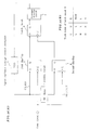
- FIG. 1 is a circuit diagram for showing a configuration of a first embodiment of the invention.
- a phase/frequency comparator circuit of this first embodiment of the invention includes the VCO1 having a frequency control terminal, the first flip-flop 2 for receiving a clock signal CLK output from the VCO1 at its data terminal and a receive data signal at its clock signal terminal C, the delay circuit 3 for delaying a clock signal output from the VCO1 by 90° to then output it, the second flip-flop 4 having its data terminal D connected with an output of the delay circuit 3 and receiving the data signal at its clock signal terminal C, the AND circuit 5 for outputting a logical product of an output of the second flip-flop 4 and a clock signal output of the delay circuit 3, the third flip-flop 6 having its clock signal terminal C connected with an output terminal of the AND circuit 5 and its data terminal D connected with an output Q of the first flip-flop 2, and the average detector circuit 7 for detecting and then outputting a time-wise average of the output Q of the third flip-flop 6, in which an output (average) of the average detector circuit 7 is fed back to the frequency control terminal of the VCO (1)
- the first through third flip-flops 2, 4, and 6 each consist of a D-type flip-flop, which samples an input at the data terminal D at a leading or trailing edge of the signal at the clock signal terminal C.
- the VCO1 may be replaced by an ICO for converting a voltage of the control signal into a current based on which an oscillation frequency thereof may be changed.
- Such a circuit as shown in FIG. 1 may be used in a reception apparatus etc. as a clock signal regenerating circuit for regenerating a clock signal from reception data, in which reception apparatus a light signal is converted at a photoelectric conversion circuit such as a photodiode into an electric signal (current) and then into a voltage, so that the receive data signal amplified to a necessary logical amplitude is input as the data signal in FIG. 1 to the clock signal terminal C of the first and second flip-flop 2 and 4.
- FIGS. 2-8 are timing charts for explaining the operations of the first embodiment.
- the clock signal CLK output from the VCO1 is delayed by 90° at the VCO1 to provide a "CLK90".
- an oscillation frequency (frequency of the clock signal CLK) of the VCO1 is called fvco and a basic frequency of the receive data signal, fdata.
- the first flip-flop 2 samples a transition edge of the clock signal CLK entered at the data terminal C at a transition edge of the data signal entered at the clock signal terminal C.
- its output Q takes on a high-and-low level random pattern due to a relationship between a set-up time and a hold time.
- the second flip-flop 4 samples the High-level V H of the clock signal CLK90 and so its Q is at the High -level V H always.
- the AND circuit 5 for the output Q of the second flip-flop 4 and CLK90 as delayed by 90° at the delay circuit 3 outputs CLK90 as it is.
- an output Vav (average voltage) of the average detector circuit 7 for time-wise averaging the output Q of the third flip-flop 6 takes on (V H +V L )/2, which is an intermediate value of the HIGH-level V H and the Low-level V L .
- the average detector circuit 7 provides a time-wise average obtained by converting a High-level duration of the output Q of the flip-flop 2 in a predetermined time period into a DC voltage level.
- it may be comprised of a low-pass filter including a CR circuit having its time constant set to a predetermined value or of a charge pump having such a configuration that the capacitor is charged at a constant current during a time when the output signal at the output terminal Q of the flip-flop 2 stays at the HIGH level and, for a period of the LOW level, is stopped in charging or discharged so that a voltage across the capacitor at a point in time when a predetermined time lapse has elapsed may be provided as a time-wise average.
- FIG. 4 is a timing chart for showing operations when the clock signal frequency fvco of the VCO1 is larger than the basic frequency fdata of the data signal (fvco>fdata).
- the cross-point of the data signal is shifted rightward with respect to output the clock signal CLK. That is, the data signal has a larger period than the clock signal CLK and so its cross-point is delayed for each cycle with respect to the transition of the trailing edge of the clock signal CLK.
- the timing the clock signal CLK is sampled at a variation point (transition edge) of the data signal is delayed (shifted rightward along the time axis in FIG. 4) for each cycle.
- the HIGH-level V H of the clock signal CLK is being sampled at the transition edge of the data signal
- the output Q of the first flip-flop 2 stays at the HIGH-level V H .
- the Low-level V L of the clock signal CLK is being sampled at the transition edge of the data signal, on the other hand, the output Q of the first flip-flop 2 stays at the Low-level V L .
- the duration of the HIGH-level V H and that of the Low-level V L of the output Q of the first flip-flop 2 alternate with each other, so that a frequency at which they cycle once is equal to a difference between the frequency fdata of the data signal and the frequency fvco of the clock signal CLK.
- the output Q of the first flip-flop 2 falls always earlier than the output of the second flip-flop 4 falls in timing.
- the output Q of the first flip-flop 2 which samples the clock signal CLK at the transition edge of the data signal takes on the LOW level in cycle t2, while the output Q of the second flip-flop 4 which samples CLK90 at the transition edge of the data signal takes on the LOW level in cycle t3.
- the AND circuit 5 outputs CLK90 only when the output Q of the second flip-flop 4 is at the HIGH-level V H . Accordingly, the output of the third flip-flop 6 takes on the High -level V H only when the outputs Q of both the first flip-flop 2 and the second flip-flop 4 are at the High-level V H .
- the output q of the first flip-flop 2 always falls earlier than the output Q of the second flip-flop 4 falls in timing.
- the output Q of the second flip-flop 4 which samples CLK90 at the transition edge of the data signal rises as delayed by 90° with respect to the output Q of the first flip-flop 2 which samples the clock signal CLK by the data signal.
- the output Q of the third flip-flop 6 provides a clock signal which has a smaller duration of being at the HIGH-level V H , so that the average detector circuit 7 outputs an intermediate value between (V H +V L )/2 and V L (see FIG. 5).
- the VCO1 receives at the frequency control terminal an average output from the average detector circuit 7 and, based on the control signal, lowers its oscillation frequency. Accordingly, the frequency fvco of the clock signal output from the VCO1 and the frequency fdata of the receive data agree with each other.
- FIG. 6 is a timing chart for showing operations in a case where the clock signal frequency of the VCO1 is lower than the basic frequency fdata of the data signal (fvco ⁇ fdata).
- the cross-point of the data signal is shifted leftward along the time axis in FIG. 6 for each cycle with respect to the clock signal CLK. That is, the clock signal CLK has a longer period than the data signal, so that the cross-point of the data signal advances in timing for each cycle with respect to the trailing transition of the clock signal CLK.
- the timing the clock signal CLK is sampled at a transition edge of the data signal is shifted forward (leftward) along the time axis for each cycle. That is, when the High-level V H of the clock signal CLK is being sampled at the transition edge of the data signal, the output Q of the first flip-flop 2 stays at the High-level VH, whereas when the LOW-level V L of the clock signal CLK is being sampled at the transition edge of the data signal, the output Q of the first flip-flop 2 stays at the Low-level V L .
- the output Q of the first flip-flop 2 becomes V H and V L levels alternately, so that a frequency at which these two levels cycle once is equal to a difference between the frequency fdata of the data signal and the frequency fvco of the clock signal CLK.
- the output Q of the first flip-flop 2 falls always later than the output of the second flip-flop 4 falls in timing.
- the AND circuit 5 outputs CLK90 only when the output Q of the second flip-flop 4 is at the HIGH-level V H . Accordingly, the output of the third flip-flop 6 takes on the HIGH-level V H only when the outputs Q of both the first flip-flop 2 and the second flip-flop 4 are at the HIGH-level V H .
- the AND circuit 5 does not output CLK90 (when the output of the second flip-flop 4 is at the Low-level V L )
- the third flip-flop 6 holds its previous state.
- the output of the first flip-flop 2 rises later by 90° than the output of the second flip-flop 4, so that the output of the third flip-flop 6 provides a clock signal which has a larger duration of being at the HIGH-level V H , which has an average between the intermediate value of (V H +V L )/2 and the HIGH-level V H .
- the frequency fvco of the VCO1 is increased.
- Fig. 8(B) is a truth table indicating a relationship between the output of the first and second flip-flops 2 and 4 and the third flip-flop 6 and FIG. 8(A), a relationship among the timing waveforms of the data signal DATA, clock signal CLK, and clock signal CLK90 delayed at the delay circuit 3 by 90° , a phase difference between the data signal DATA and the clock signal CLK (a phase difference of 0 means phase agreement), and the output of the third flip-flop 6.
- the output of the third flip-flop 6 takes on the LOW-level V L .
- the third flip-flop6 holds the previous state of the High- or Low-level V H or V L .
- the third flip-flop 6 holds the Low-level output as has been in the interval A and, over a transition from the interval B to the interval C, holds the Low-level output as has been in the interval B.
- the third flip-flop 6 When a transition is made from the interval D to the interval C, the third flip-flop 6 holds the HIGH-level output as has been in the interval D, when a transition is made from the interval C to the interval B, it holds the HIGH-level output as has been the interval C, and when a transition is made from the interval B to the interval A, it provides the Low-level output.
- a directivity such as indicated by an arrow
- Such a comparison example as against this embodiment may be assumed in which a difference between the clock signal CLK and the data signal DATA is detected by only one flip-flop (e.g., the second flip-flop 2 in FIG. 1); in this case, a phase ( ⁇ 180°) at a transition of the output of this flip-flop from the LOW to HIGH levels agrees with a phase ( ⁇ 180°) at a transition from the HIGH to LOW levels to provide no hysteresis property, thus enabling correctly detecting only up to a phase difference less than ⁇ 180°.
- FIG. 9 is a circuit diagram for showing a configuration of the second embodiment of the invention.
- this embodiment uses the latch circuit 8 to replace the AND circuit 5 and the third flip-flop 6 (edge-trigger type D-flip-flop) as its feature.
- the latch circuit 8 consists of a level-sense type D-latch, acting to hold the previous state when the clock signal terminal C is at the Low-level and output as it is a state input at the data terminal when the clock signal terminal is at the High-level as shown in the truth table of FIG. 9(B).
- the latch circuit 8 combines in operation the AND circuit 5 and the third flip-flop 6 shown in FIG. 1. Moreover, the latch circuit 8 can be realized in a half the circuit scale of the third flip-flop 6, thus effectively contributing the miniaturization and power-dissipation saving. Like the above-mentioned embodiment, this embodiment also provides a width between a phase at a transition from the output of the latch circuit 8 from the LOW to HIGH levels and a phase at a transition from the HIGH to LOW levels, thus enabling correctly detecting a phase difference of up to ⁇ 270.
- the configuration of the invention has two functions; a function to detect whether two signals are synchronized with each other in frequency to then feed back a detection result in the control signal to a signal oscillator comprised of a VCO or ICO so that the two signals may agree in frequency and another to detect a phase difference between two signals which agreed in frequency to then feed back a detection result in the control signal to the signal oscillator so that they may agree in phase.
- the invention may not only be applied to a reception apparatus but also may be applied as it is as a phase/frequency comparator circuit in a PLL circuit for inputting a standard clock signal and outputting a signal synchronized with this reference clock signal. That is, by providing such a PLL circuit that, in the circuit described with the above-mentioned first embodiment which includes the first flip-flop 2, the delay circuit 3, the second flip-flop 4, the AND circuit 5, and the third flip-flop 6 or the circuit which includes the first flip-flop 2, the delay circuit 3, the second flip-flop 4, and the latch circuit 8, an output of the third flip-flop 6 or the latch circuit 8 respectively is smoothed into a DC voltage by the loop filter (or the average detector circuit 7), which is in turn supplied as a control signal to the VCO, a clock signal output from which is then directly given or frequency-divided by a frequency divider circuit to provide the clock signal CLK, which is input to the data terminal D of the first flip-flop 2 in the phase/frequency comparator circuit while at the same time the
- the invention gives an effect of simplifying a circuit configuration because a phase/frequency comparator circuit can be comprised of the first flip-flop which samples a clock signal output of the VCO at a trailing or leading edge of the data signal, the second flip-flop which samples the clock signal output as delayed by a predetermined phase at the trailing or leading edge of the data signal, the third flip-flop which samples an output of the first flip-flop at a transition edge of an AND signal obtained by AND'ing an output of the second flip-flop and the delayed clock signal output, and the average detector circuit which detects an output of the third flip-flop.
- the invention it is possible to feed back in configuration an output of the average detector circuit to the VCO at its frequency control terminal to thereby control an oscillation frequency of the VCO, thus generating a clock signal synchronized with the data signal.
- phase synchronization control can be conducted so that they may agree in phase.
Landscapes
- Engineering & Computer Science (AREA)
- Power Engineering (AREA)
- Computer Networks & Wireless Communication (AREA)
- Signal Processing (AREA)
- Stabilization Of Oscillater, Synchronisation, Frequency Synthesizers (AREA)
- Synchronisation In Digital Transmission Systems (AREA)
- Dc Digital Transmission (AREA)
- Optical Communication System (AREA)
- Manipulation Of Pulses (AREA)
Abstract
Description
Claims (16)
- A phase/frequency comparator circuit for comparing a first and second signals to each other in terms of frequency and phase, comprising:a first sequential logical circuit for sampling and outputting said second signal at a leading or trailing edge of said first signal;a delay circuit for delaying said second signal by a predetermined phase;a second sequential logical circuit for sampling and outputting said second signal as delayed at said delay circuit, at a leading or trailing edge of said first signal; anda third sequential logical circuit for sampling and outputting an output of said sequential logical circuit at a leading or trailing edge of a signal of a logical product of an output of said second sequential logical circuit and said second signal delayed at said delay circuit.
- A phase/frequency comparator circuit for comparing a first and second signals to each other in terms of frequency and phase, comprising:a first sequential logical circuit for sampling and outputting said second signal at a leading or trailing edge of said first signal;a delay circuit for delaying said second signal by a predetermined phase;a second sequential logical circuit for sampling and outputting said second signal as delayed at said delay circuit, at a leading or trailing edge of said first signal; anda third sequential logical circuit for receiving as an input the outputs of said first and second sequential logical circuits to provide an output of said first sequential logical circuit when said second sequential logical circuit provides an output having a first value of signal level and holds the previous value when the second sequential logical circuit provides an output having a second value of signal level.
- The phase/frequency comparator circuit according to Claim 1, wherein said first through third sequential logical circuits respectively comprise a first through third flip-flops for sampling a signal input at a data input terminal, at a leading or trailing edge of a signal input at a clock signal input terminal.
- The phase/frequency comparator circuit according to Claim 2, wherein:said first and second sequential logical circuits respectively comprise a first and second flip-flops for sampling a signal input at a data input terminal, at a leading or trailing edge of a signal input at a clock signal input terminal; andsaid third sequential logical circuit is comprised of a latch circuit for providing, as is ,a signal input at said data input terminal from an output terminal thereof when a signal input at said clock signal input terminal has a first value of signal level and holding the previous value at said output terminal when said signal input at said clock signal input terminal has a second value of signal level.
- The phase/frequency comparator circuit according to any one of Claims 1 through 4, wherein said delay circuit delays a phase of said second signal by a half of a pulse width of said second signal.
- The phase/frequency comparator circuit according to any one of Claims 1 through 4, wherein said delay circuit delays a phase of said second signal by 90°.
- The phase/frequency comparator circuit according to any one of Claims 1 through 6, further comprising an average detector circuit for detecting and outputting an average of the output of said third sequential logical circuit.
- the phase/frequency comparator circuit according to Claim 7, wherein said average detector circuit outputs as said average a DC voltage indicating a time lapse over which a signal input to said average detector circuit holds a first or second value in a predetermined time period.
- A clock signal regenerating circuit, comprising:a phase/frequency comparator circuit as claimed in Claim 7 or 8; anda signal oscillator comprised of a voltage control oscillator or a current control oscillator for changing an oscillation frequency based on a frequency control signal input at a frequency control terminal to then output a clock signal having said oscillation frequency, wherein:a clock signal output from said signal oscillator is fed as said second signal to said phase/frequency comparator circuit, a reception data signal is fed as said first signal to said phase/frequency comparator circuit, and an output of said average detector circuit is fed as said frequency control signal to said frequency control terminal of said signal oscillator; andsaid signal oscillator then outputs a clock signal synchronized with said reception data signal.
- A light reception apparatus comprising:a phase/frequency comparator circuit as claimed in Claim 7 or 8; anda signal oscillator comprised of a voltage control oscillator or a current control oscillator for changing an oscillation frequency based on a frequency control signal input at a frequency control terminal to then output a clock signal having said oscillation frequency, wherein:a clock signal output from said signal oscillator is fed as said second signal to said phase/frequency comparator circuit;a reception data signal converted into an electric signal through photoelectric conversion means for receiving a light signal is fed as said first signal to said phase/frequency comparator circuit, while an output of said average detector circuit is fed as said frequency control signal to said frequency control terminal of said signal oscillator; andsaid signal oscillator then outputs a clock signal synchronized with said reception data signal.
- A PLL circuit comprising:a phase/frequency comparator circuit as claimed in any one of Claims 1 through 6; anda signal oscillator comprised of a voltage control oscillator or a current control oscillator for changing an oscillation frequency based on a frequency control signal input at a frequency control terminal to then output a clock signal having said oscillation frequency, wherein:an oscillation clock signal output from said signal oscillator is fed directly to or frequency-divided at a frequency divider circuit and then fed said phase/frequency comparator circuit as said second signal;an incoming reference signal is fed to said phase/frequency comparator circuit as said first signal; andan output of said third sequential logical circuit in said phase/frequency comparator circuit is fed through a loop filter to said frequency control terminal of said signal oscillator as said frequency control signal, so that said signal oscillator or said frequency divider circuit outputs a clock signal synchronized with said reference signal.
- A clock signal regenerating circuit comprising:wherein an average output from said average detector circuit is fed back to said frequency terminal of said voltage control oscillator to thereby control an oscillation frequency of said voltage control oscillator, thus generating a clock signal synchronized with said data signal.a voltage control oscillator having a frequency control terminal, for oscillating a frequency which corresponding to a control voltage applied at said frequency control terminal;a first flip-flop for receiving as an input a clock signal output of said voltage control oscillator at a data input terminal and also receiving an incoming data signal at a clock signal input terminal, for sampling a clock signal output from said voltage control oscillator to then output said clock signal from an output terminal;a delay circuit for delaying said clock signal output from said voltage control oscillator by a predetermined phase to then output said clock signal;a second flip-flop receiving as an input said clock signal delayed by said delay circuit and also receiving said data signal at a clock signal input terminal, for sampling said clock signal delayed by said delay circuit at leading or trailing edge of said data signal to then output said clock signal from said output terminal;a logical product circuit for AND'ing an output of said second flip-flop and said clock signal delayed by said delay circuit to then output a resultant logical product;a third flip-flop receiving as an input an output of said first flip-flop at said data input terminal and also receiving an output of said logical product circuit at said clock signal input terminal, for sampling an output of said first flip-flop at a leading or trailing edge of an output of said logical product circuit to then provide said output from said output terminal; andan average detector circuit for detecting an average of an output of said third flip-flop,
- A clock signal regenerating circuit comprising:wherein an average output from said average detector circuit is fed back to said frequency terminal of said voltage control oscillator to thereby control an oscillation frequency of said voltage control oscillator, thus generating a clock signal synchronized with said data signal.a voltage control oscillator having a frequency control terminal, for oscillating a frequency which corresponding to a control voltage applied at said frequency control terminal;a first flip-flop for receiving as an input a clock signal output of said voltage control oscillator at a data input terminal and also receiving an incoming data signal at a clock signal input terminal, for sampling a clock signal output from said voltage control oscillator to then output said clock signal from an output terminal;a delay circuit for delaying said clock signal output from said voltage control oscillator by a predetermined phase to then output said clock signal;a second flip-flop receiving as an input said clock signal delayed by said delay circuit and also receiving said data signal at a clock signal input terminal, for sampling said clock signal delayed by said delay circuit at leading or trailing edge of said data signal to then output said clock signal from said output terminal;a latch circuit receiving as an input an output of said first flip-flop and an output of said second flip-flop, for providing an output of said flip-flop as it is from an output terminal when said second flip-flop gives a first value of output level and holding the previous value when said second flip-flop gives a second value of output level; andan average detector circuit for detecting an average of an output of said third flip-flop,
- The clock signal regenerating circuit according to Claim 12 or 13, wherein said delay circuit delays a phase of said clock signal by a phase which corresponds to a half of a pulse width of said clock signal pulse.
- The clock signal regenerating circuit according to Claim 12 or 13, wherein said delay circuit delays a phase of said clock signal by 90°.
- The clock signal regenerating circuit according to Claim 12 or 13, wherein said average detector circuit outputs as said average a DC current which indicates a time lapse over which a signal input to said average detector circuit holds a first or second value in a predetermined time period.
Applications Claiming Priority (2)
| Application Number | Priority Date | Filing Date | Title |
|---|---|---|---|
| JP2000319748 | 2000-10-19 | ||
| JP2000319748A JP3630092B2 (en) | 2000-10-19 | 2000-10-19 | Phase frequency comparison circuit |
Publications (2)
| Publication Number | Publication Date |
|---|---|
| EP1199804A2 true EP1199804A2 (en) | 2002-04-24 |
| EP1199804A3 EP1199804A3 (en) | 2004-01-07 |
Family
ID=18798154
Family Applications (1)
| Application Number | Title | Priority Date | Filing Date |
|---|---|---|---|
| EP01125042A Withdrawn EP1199804A3 (en) | 2000-10-19 | 2001-10-15 | Phase/frequency comparator |
Country Status (4)
| Country | Link |
|---|---|
| US (1) | US20020051510A1 (en) |
| EP (1) | EP1199804A3 (en) |
| JP (1) | JP3630092B2 (en) |
| CA (1) | CA2359270C (en) |
Cited By (4)
| Publication number | Priority date | Publication date | Assignee | Title |
|---|---|---|---|---|
| US8704563B2 (en) | 2008-11-17 | 2014-04-22 | Infineon Technologies Ag | Phase-lock loop |
| US8953722B2 (en) | 2007-11-27 | 2015-02-10 | Infineon Technologies Ag | Controlled transmission of data in a data transmission system |
| WO2022037216A1 (en) * | 2020-08-20 | 2022-02-24 | 长鑫存储技术有限公司 | Detection circuit and detection method |
| US11402431B2 (en) | 2020-08-20 | 2022-08-02 | Changxin Memory Technologies, Inc. | Detection circuit and detection method |
Families Citing this family (17)
| Publication number | Priority date | Publication date | Assignee | Title |
|---|---|---|---|---|
| JP3418712B2 (en) * | 2000-09-29 | 2003-06-23 | 富士通カンタムデバイス株式会社 | Phase comparison circuit |
| US7068086B2 (en) * | 2001-07-27 | 2006-06-27 | Advantest Corp. | Phase correction circuit |
| JP3637014B2 (en) | 2001-11-21 | 2005-04-06 | 日本電気株式会社 | Clock synchronization loss detection circuit and optical receiver using the same |
| US7609797B2 (en) * | 2003-09-04 | 2009-10-27 | Standard Microsystems Corporation | Circuit, system, and method for preventing a communication system absent a dedicated clocking master from producing a clocking frequency outside an acceptable range |
| ATE470268T1 (en) * | 2004-03-29 | 2010-06-15 | Nxp Bv | FAST PHASE FREQUENCY DETECTOR ARRANGEMENT |
| US7535985B2 (en) * | 2004-04-26 | 2009-05-19 | Panasonic Corporation | Resynchronization circuit |
| JP4271623B2 (en) * | 2004-06-17 | 2009-06-03 | 富士通株式会社 | Clock adjustment apparatus and method |
| JP4948077B2 (en) * | 2005-10-14 | 2012-06-06 | ルネサスエレクトロニクス株式会社 | Transceiver and communication system using the same |
| US8248104B2 (en) | 2007-09-14 | 2012-08-21 | Nec Corporation | Phase comparator and phase-locked loop |
| US7764088B2 (en) * | 2008-09-24 | 2010-07-27 | Faraday Technology Corp. | Frequency detection circuit and detection method for clock data recovery circuit |
| US9184733B2 (en) * | 2013-03-15 | 2015-11-10 | Qualcomm Incorporated | Low power architectures |
| JP6582771B2 (en) | 2015-09-09 | 2019-10-02 | 富士通株式会社 | Signal reproduction circuit, electronic device, and signal reproduction method |
| JP6772477B2 (en) | 2016-02-18 | 2020-10-21 | 富士通株式会社 | Signal reproduction circuit, electronic device and signal reproduction method |
| JP6724619B2 (en) | 2016-07-15 | 2020-07-15 | 富士通株式会社 | Signal reproducing circuit, electronic device and signal reproducing method |
| RU2647678C1 (en) * | 2017-06-13 | 2018-03-16 | Федеральное государственное бюджетное образовательное учреждение высшего образования "Омский государственный технический университет" | Frequency-phase comparator |
| US11424903B1 (en) * | 2019-08-08 | 2022-08-23 | Synopsys, Inc. | Drift tracking using an analog delay line during clock-data recovery |
| CN113740717B (en) * | 2020-05-29 | 2025-06-03 | 深圳市中兴微电子技术有限公司 | A method and circuit for measuring the holding time of a timing unit |
Family Cites Families (9)
| Publication number | Priority date | Publication date | Assignee | Title |
|---|---|---|---|---|
| US3585640A (en) * | 1969-05-19 | 1971-06-22 | Angelica Corp | Garment |
| US4377728A (en) * | 1981-03-04 | 1983-03-22 | Motorola Inc. | Phase locked loop with improved lock-in |
| US5694088A (en) * | 1996-07-08 | 1997-12-02 | Maxim Integrated Products, Inc. | Phase locked loop with improved phase-frequency detection |
| DE19630917C1 (en) * | 1996-07-31 | 1998-03-26 | Siemens Ag | Phase and frequency detector circuit |
| US6081572A (en) * | 1998-08-27 | 2000-06-27 | Maxim Integrated Products | Lock-in aid frequency detector |
| US6177843B1 (en) * | 1999-05-26 | 2001-01-23 | Cypress Semiconductor Corp. | Oscillator circuit controlled by programmable logic |
| US6577694B1 (en) * | 1999-11-08 | 2003-06-10 | International Business Machines Corporation | Binary self-correcting phase detector for clock and data recovery |
| US6909852B2 (en) * | 2000-02-17 | 2005-06-21 | Broadcom Corporation | Linear full-rate phase detector and clock and data recovery circuit |
| US6285219B1 (en) * | 2000-03-30 | 2001-09-04 | Adaptec, Inc. | Dual mode phase and frequency detector |
-
2000
- 2000-10-19 JP JP2000319748A patent/JP3630092B2/en not_active Expired - Fee Related
-
2001
- 2001-10-09 US US09/971,922 patent/US20020051510A1/en not_active Abandoned
- 2001-10-15 EP EP01125042A patent/EP1199804A3/en not_active Withdrawn
- 2001-10-18 CA CA002359270A patent/CA2359270C/en not_active Expired - Fee Related
Cited By (6)
| Publication number | Priority date | Publication date | Assignee | Title |
|---|---|---|---|---|
| US8953722B2 (en) | 2007-11-27 | 2015-02-10 | Infineon Technologies Ag | Controlled transmission of data in a data transmission system |
| US8704563B2 (en) | 2008-11-17 | 2014-04-22 | Infineon Technologies Ag | Phase-lock loop |
| DE102009052481B4 (en) * | 2008-11-17 | 2015-04-30 | Infineon Technologies Ag | Phase-locked loop |
| US9608645B2 (en) | 2008-11-17 | 2017-03-28 | Infineon Technologies Ag | Phase-lock loop |
| WO2022037216A1 (en) * | 2020-08-20 | 2022-02-24 | 长鑫存储技术有限公司 | Detection circuit and detection method |
| US11402431B2 (en) | 2020-08-20 | 2022-08-02 | Changxin Memory Technologies, Inc. | Detection circuit and detection method |
Also Published As
| Publication number | Publication date |
|---|---|
| EP1199804A3 (en) | 2004-01-07 |
| CA2359270C (en) | 2005-01-11 |
| JP2002135093A (en) | 2002-05-10 |
| US20020051510A1 (en) | 2002-05-02 |
| JP3630092B2 (en) | 2005-03-16 |
| CA2359270A1 (en) | 2002-04-19 |
Similar Documents
| Publication | Publication Date | Title |
|---|---|---|
| CA2359270C (en) | Phase/frequency comparator | |
| US6081572A (en) | Lock-in aid frequency detector | |
| US6642747B1 (en) | Frequency detector for a phase locked loop system | |
| JP3649194B2 (en) | PLL circuit and optical communication receiver | |
| US5557648A (en) | Phase lock loop circuit using a sample and hold switch circuit | |
| US8315349B2 (en) | Bang-bang phase detector with sub-rate clock | |
| EP1199805B1 (en) | PLL circuit and optical communication reception apparatus | |
| JP2010193493A (en) | Initialization circuit for delay locked loop | |
| US6496555B1 (en) | Phase locked loop | |
| JP3623948B2 (en) | Burst mode receiving apparatus resistant to noise and its clock signal and data recovery method | |
| JP3327249B2 (en) | PLL circuit | |
| US6636090B2 (en) | Phase-locked loop circuit outputting clock signal having fixed phase difference with respect to input clock signal | |
| JP3617456B2 (en) | PLL circuit and optical communication receiver | |
| US7109806B2 (en) | Device and method for detecting phase difference and PLL using the same | |
| CN102055469B (en) | Phase discriminator and phase locked loop circuit | |
| US7397881B2 (en) | Erroneous phase lock detection circuit | |
| JP2002094494A (en) | Clock recovery circuit | |
| US7598816B2 (en) | Phase lock loop circuit with delaying phase frequency comparson output signals | |
| GB2336732A (en) | Frequency comparator and PLL circuit using the same | |
| JP2005086789A (en) | Clock data recovery circuit | |
| JP3994545B2 (en) | Data receiver | |
| JP3810185B2 (en) | Synchronous oscillation circuit | |
| US6647079B1 (en) | Surface acoustic wave-based clock and data recovery circuit | |
| KR20010036433A (en) | Phase locked loop circuit | |
| KR940006093Y1 (en) | Digital phase locked loop circuit |
Legal Events
| Date | Code | Title | Description |
|---|---|---|---|
| PUAI | Public reference made under article 153(3) epc to a published international application that has entered the european phase |
Free format text: ORIGINAL CODE: 0009012 |
|
| AK | Designated contracting states |
Kind code of ref document: A2 Designated state(s): AT BE CH CY DE DK ES FI FR GB GR IE IT LI LU MC NL PT SE TR |
|
| AX | Request for extension of the european patent |
Free format text: AL;LT;LV;MK;RO;SI |
|
| PUAL | Search report despatched |
Free format text: ORIGINAL CODE: 0009013 |
|
| AK | Designated contracting states |
Kind code of ref document: A3 Designated state(s): AT BE CH CY DE DK ES FI FR GB GR IE IT LI LU MC NL PT SE TR |
|
| AX | Request for extension of the european patent |
Extension state: AL LT LV MK RO SI |
|
| 17P | Request for examination filed |
Effective date: 20031126 |
|
| AKX | Designation fees paid |
Designated state(s): DE FR |
|
| 17Q | First examination report despatched |
Effective date: 20050204 |
|
| STAA | Information on the status of an ep patent application or granted ep patent |
Free format text: STATUS: THE APPLICATION HAS BEEN WITHDRAWN |
|
| 18W | Application withdrawn |
Effective date: 20050603 |