EP1199790A2 - Power supply pulse width modulation (PWM) control system - Google Patents
Power supply pulse width modulation (PWM) control system Download PDFInfo
- Publication number
- EP1199790A2 EP1199790A2 EP01000524A EP01000524A EP1199790A2 EP 1199790 A2 EP1199790 A2 EP 1199790A2 EP 01000524 A EP01000524 A EP 01000524A EP 01000524 A EP01000524 A EP 01000524A EP 1199790 A2 EP1199790 A2 EP 1199790A2
- Authority
- EP
- European Patent Office
- Prior art keywords
- pwm
- power supply
- control system
- signal
- pmos transistor
- Prior art date
- Legal status (The legal status is an assumption and is not a legal conclusion. Google has not performed a legal analysis and makes no representation as to the accuracy of the status listed.)
- Granted
Links
- 230000007704 transition Effects 0.000 claims abstract description 10
- 239000003990 capacitor Substances 0.000 claims description 30
- 230000004044 response Effects 0.000 claims description 14
- 230000000694 effects Effects 0.000 claims description 12
- 238000004891 communication Methods 0.000 claims description 4
- 238000007599 discharging Methods 0.000 claims 1
- 230000001934 delay Effects 0.000 abstract description 6
- 238000000034 method Methods 0.000 description 13
- 238000010586 diagram Methods 0.000 description 10
- 208000028659 discharge Diseases 0.000 description 8
- 230000006870 function Effects 0.000 description 8
- 230000008901 benefit Effects 0.000 description 6
- 230000003071 parasitic effect Effects 0.000 description 4
- 230000008878 coupling Effects 0.000 description 3
- 238000010168 coupling process Methods 0.000 description 3
- 238000005859 coupling reaction Methods 0.000 description 3
- 238000004519 manufacturing process Methods 0.000 description 3
- 238000012546 transfer Methods 0.000 description 3
- 230000003321 amplification Effects 0.000 description 2
- 230000006399 behavior Effects 0.000 description 2
- 230000008859 change Effects 0.000 description 2
- 238000013461 design Methods 0.000 description 2
- 238000005516 engineering process Methods 0.000 description 2
- 238000012986 modification Methods 0.000 description 2
- 230000004048 modification Effects 0.000 description 2
- 238000003199 nucleic acid amplification method Methods 0.000 description 2
- 230000000630 rising effect Effects 0.000 description 2
- 235000008694 Humulus lupulus Nutrition 0.000 description 1
- 230000004075 alteration Effects 0.000 description 1
- 230000015556 catabolic process Effects 0.000 description 1
- 238000006243 chemical reaction Methods 0.000 description 1
- 238000010276 construction Methods 0.000 description 1
- 230000007812 deficiency Effects 0.000 description 1
- 238000006731 degradation reaction Methods 0.000 description 1
- 230000001747 exhibiting effect Effects 0.000 description 1
- 230000036039 immunity Effects 0.000 description 1
- 230000010354 integration Effects 0.000 description 1
- 230000006386 memory function Effects 0.000 description 1
- 235000002020 sage Nutrition 0.000 description 1
- 230000035945 sensitivity Effects 0.000 description 1
- 238000006467 substitution reaction Methods 0.000 description 1
Images



Classifications
-
- H—ELECTRICITY
- H02—GENERATION; CONVERSION OR DISTRIBUTION OF ELECTRIC POWER
- H02M—APPARATUS FOR CONVERSION BETWEEN AC AND AC, BETWEEN AC AND DC, OR BETWEEN DC AND DC, AND FOR USE WITH MAINS OR SIMILAR POWER SUPPLY SYSTEMS; CONVERSION OF DC OR AC INPUT POWER INTO SURGE OUTPUT POWER; CONTROL OR REGULATION THEREOF
- H02M7/00—Conversion of AC power input into DC power output; Conversion of DC power input into AC power output
- H02M7/42—Conversion of DC power input into AC power output without possibility of reversal
- H02M7/44—Conversion of DC power input into AC power output without possibility of reversal by static converters
- H02M7/48—Conversion of DC power input into AC power output without possibility of reversal by static converters using discharge tubes with control electrode or semiconductor devices with control electrode
- H02M7/505—Conversion of DC power input into AC power output without possibility of reversal by static converters using discharge tubes with control electrode or semiconductor devices with control electrode using devices of a thyratron or thyristor type requiring extinguishing means
- H02M7/515—Conversion of DC power input into AC power output without possibility of reversal by static converters using discharge tubes with control electrode or semiconductor devices with control electrode using devices of a thyratron or thyristor type requiring extinguishing means using semiconductor devices only
- H02M7/525—Conversion of DC power input into AC power output without possibility of reversal by static converters using discharge tubes with control electrode or semiconductor devices with control electrode using devices of a thyratron or thyristor type requiring extinguishing means using semiconductor devices only with automatic control of output waveform or frequency
- H02M7/527—Conversion of DC power input into AC power output without possibility of reversal by static converters using discharge tubes with control electrode or semiconductor devices with control electrode using devices of a thyratron or thyristor type requiring extinguishing means using semiconductor devices only with automatic control of output waveform or frequency by pulse width modulation
- H02M7/529—Conversion of DC power input into AC power output without possibility of reversal by static converters using discharge tubes with control electrode or semiconductor devices with control electrode using devices of a thyratron or thyristor type requiring extinguishing means using semiconductor devices only with automatic control of output waveform or frequency by pulse width modulation using digital control
-
- H—ELECTRICITY
- H03—ELECTRONIC CIRCUITRY
- H03K—PULSE TECHNIQUE
- H03K7/00—Modulating pulses with a continuously-variable modulating signal
- H03K7/08—Duration or width modulation ; Duty cycle modulation
-
- H—ELECTRICITY
- H02—GENERATION; CONVERSION OR DISTRIBUTION OF ELECTRIC POWER
- H02M—APPARATUS FOR CONVERSION BETWEEN AC AND AC, BETWEEN AC AND DC, OR BETWEEN DC AND DC, AND FOR USE WITH MAINS OR SIMILAR POWER SUPPLY SYSTEMS; CONVERSION OF DC OR AC INPUT POWER INTO SURGE OUTPUT POWER; CONTROL OR REGULATION THEREOF
- H02M1/00—Details of apparatus for conversion
- H02M1/08—Circuits specially adapted for the generation of control voltages for semiconductor devices incorporated in static converters
-
- H—ELECTRICITY
- H02—GENERATION; CONVERSION OR DISTRIBUTION OF ELECTRIC POWER
- H02M—APPARATUS FOR CONVERSION BETWEEN AC AND AC, BETWEEN AC AND DC, OR BETWEEN DC AND DC, AND FOR USE WITH MAINS OR SIMILAR POWER SUPPLY SYSTEMS; CONVERSION OF DC OR AC INPUT POWER INTO SURGE OUTPUT POWER; CONTROL OR REGULATION THEREOF
- H02M3/00—Conversion of DC power input into DC power output
- H02M3/02—Conversion of DC power input into DC power output without intermediate conversion into AC
- H02M3/04—Conversion of DC power input into DC power output without intermediate conversion into AC by static converters
- H02M3/10—Conversion of DC power input into DC power output without intermediate conversion into AC by static converters using discharge tubes with control electrode or semiconductor devices with control electrode
- H02M3/145—Conversion of DC power input into DC power output without intermediate conversion into AC by static converters using discharge tubes with control electrode or semiconductor devices with control electrode using devices of a triode or transistor type requiring continuous application of a control signal
- H02M3/155—Conversion of DC power input into DC power output without intermediate conversion into AC by static converters using discharge tubes with control electrode or semiconductor devices with control electrode using devices of a triode or transistor type requiring continuous application of a control signal using semiconductor devices only
- H02M3/156—Conversion of DC power input into DC power output without intermediate conversion into AC by static converters using discharge tubes with control electrode or semiconductor devices with control electrode using devices of a triode or transistor type requiring continuous application of a control signal using semiconductor devices only with automatic control of output voltage or current, e.g. switching regulators
Definitions
- This invention relates generally to power supply pulse width modulation (PWM) control systems and methods, and more particularly to a power supply PWM method and system that uses peak current program mode (CPM) control for large duty ratios with a smooth transition to voltage mode control at small duty ratios down to zero duty ratio.
- PWM pulse width modulation
- CCM peak current program mode
- CPM Current program mode
- the duty ratio is determined when the switch current reaches a peak value that is requested by a control voltage.
- the control voltage is a compensated version of the error between a power supply output voltage and a fixed reference.
- the switch current and the requested peak current are larger than the noise in the system, and they are sufficiently centered between comparator supply voltages and error-amplifier supply voltages in order to have smooth operation at large duty ratios and large currents.
- a small duty ratio is required however, (i.e., below a few percent), the current sense signal becomes too small and too close to ground for the PWM comparator to successfully distinguish the greater of the current sense signal and the control voltage signal.
- PWM pulse width modulation
- the present invention is directed to a power supply PWM control technique that uses peak current program mode (CPM) control for large duty ratios with a smooth transition to voltage mode control at small duty ratios down to zero duty ratio and that improves the speed of modulation.
- a PWM comparator is implemented so that it operates in three different modes, depending on the current sense level.
- the PWM comparator performs CPM control (first mode) over most of the control range where the current sense levels are large.
- the PWM comparator performs voltage mode control (second mode), causing the duty ratio to be proportional to the control voltage.
- Voltage mode control is where the duty ratio is determined by a voltage or voltage error signal.
- the PWM comparator has a small operating range where the first and second modes overlap in order to facilitate a smooth transition between CPM and voltage mode control ranges.
- a third mode of operation occurs when the control voltage becomes low enough to drive the duty ratio to zero without any intermittent pulses.
- a power supply PWM control technique is implemented using an unbalanced comparator and relying on a cut-off threshold in order to determine the mode of modulation.
- a power supply PWM control technique is implemented additionally using a differential amplifier in order to achieve balanced operation for high noise immunity at high speeds.
- a power supply PWM technique is implemented using another differential amplifier whose purpose is to set the point where the mode of modulation changes by a reference instead of relying on parasitic cut-off thresholds.
- a power supply PWM technique is implemented using a capacitor to store the state of the modulator in contrast to the PWM latch.
- a power supply PWM technique is implemented in which the PWM controller smoothly transitions from a first mode through a third mode and back so that the power supply output remains smoothly controlled.
- a power supply PWM technique is implemented in which the amount of delay is greatly reduced due to the size of the PWM state capacitor and its functional location.
- FIG 1 is a schematic diagram illustrating an ideal current program mode pulse width modulated switched mode converter 10 that is discussed herein below to better illustrate the advantages provided by aspects of the present invention depicted in Figures 4-6.
- the Control Voltage 102 shown in Figure 1 simply sets the peak current level in switch Q 1 104.
- Figure 2 illustrates signal waveforms associated with the ideal current program mode pulse width modulated switched mode converter 10 shown in Figure 1.
- Duty ratio 'D' 200 is the time duration that switch Q 1 104 is ON during a switch cycle divided by the duration of that cycle, determined by CLOCK 202. The duty ratio is related to how much energy is transferred from power source input Vg 106 to R Load 108. Higher duty ratios result in a higher energy transfer from the source Vg 106 to R Load 108.
- the bias connection 112 to ground on the PWM comparator 114 is the only non-ideal condition that is depicted in Figure 1. Regarding a practical implementation, this connection 112 results in the PWM comparator 114 losing sensitivity when either or both the Control Voltage signal 102 and the Current Sense signal 110 are close to the bias connection 112 voltage (ground in this case). Performance degradation typically occurs at levels below 200mV.
- the pulse width 204 is wide during the range 0 ⁇ t ⁇ 3 T s , and the Current Sense signal 110 level is well above the ground bias level. Wider duty ratios ultimately result in larger signals due to higher energy transfer. At narrower duty ratios however, (in the range 3 T s ⁇ t ⁇ 6 T s ), the Current Sense signal 110 level is small, and perhaps close enough to the ground bias level that the PWM comparator 114 has difficulty in correctly distinguishing which signal is larger.
- FIG. 3 is a schematic diagram illustrating a prior art high speed PWM comparator 300 and PWM latch 302.
- the first stage of the PWM comparator 300 includes M1, M2, M3, M4 and A1 to implement a differential amplifier 303 whose output voltage V G6 304 is proportional to the difference between the input voltages V S 306 (Current Sense) and V C 308 (Control Voltage).
- the gain of the first stage differential amplifier 303 is however, large enough so that the differential amplifier 303 saturates.
- the second stage 310 includes M6 and A2 which together inverts and amplifies the signal V G6 304. Current source A2 causes the rising edge of V D6 312.
- the third stage 314 includes inverter I1 that inverts signal V D6 312 and resets PWM latch 302.
- the duration between the set signal, V CK 316, and the reset signal 318 is the ON duration 320, as shown in signal V M 322.
- Inverter I1 also serves as a low impedance buffer between the amplification stage 310 and the logic stages in PWM latch 302.
- the prior art high speed PWM comparator 300 and PWM latch 302 combine to formulate a system that is robust to noise, but suffers from delays that are imposed by PWM latch 302.
- An offset to V G6 304 must be incorporated in order for the comparator 300 and latch 302 to function properly. Generally, this offset is implemented by selecting M2 to have much larger gain and drain-source admittance than M1. Further, the differential amplifier 303 gain must be high in order to supply enough signal to cross the thresholds of inverter I1. High gain is a conflicting requirement with high speed. Further, the digital nature of the PWM Comparator 300 and PWM Latch 302 in this implementation causes the output V M 322 to suddenly lose signal when V S 306 and V C 308 become small signals. This characteristic will cause pulse skipping at low duty ratios.
- the PWM Comparator 300 and PWM Latch 302 schemes depicted in Figure 3 have been problematic when operating at low duty ratios. Specifically, two deficiencies associated with this scheme can cause pulse skipping while operating at a low duty ratio. These are 1) insufficient signals and 2) delay. High gain in the differential stage 303 is achieved at the expense of speed. Insufficient signals occur at narrow duty ratios because the slope of the current sense signal 306 is very low which results in a small differential signal. The differential signal V G6 304 can be too small to activate M6, thus causing a pulse to be skipped. An insufficient signal can be easily contaminated with stray couplings that make the skipping problem worse. Delay causes duty cycle skipping in the following manner.
- the differential amplifier 303 requires time to settle after the rising edge of V S 306 in order to make an accurate comparison between V S 306 and V C 308.
- the latch 302 requires set-up time and it imposes delays due to its internal logic gates and feedback. A pulse will be skipped on the switch cycle following a command for a narrower pulse than the delay through the comparator 300 and the latch 302.
- the prior art comparator 300 and latch 302 therefore have a minimum duty ratio below which the duty ratio falls to zero.
- the performance and offsets of the differential amplifier 303 depend on parasitic couplings that are distributed in the circuit between VDD, A1, M1, M2, M3 and M4. Many of the parasitic features vary substantially over temperature and over manufacturing process. The performance of this topology scheme at narrow duty ratios is inconsistent over temperature and manufacturing lots. Imposing a positive offset on V G6 304 in order to reduce the amount that V G6 304 goes below the threshold of M6 can reduce the minimum duty ratio effect. Intentionally making M2 have more gain than M1 is the typical method for achieving an offset. The unbalanced technique is limited however, due to variations in the parasitic devices and the drawback that unbalanced operation increases the effects of noise.
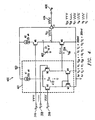
- FIG. 4 is a schematic diagram illustrating a PWM comparator 400 with its latching function performed by a capacitor 402 according to one embodiment of the present invention.
- the scheme depicted in Figure 4 functions to make the duty cycle control range smooth by implementing the memory function of the latch as an analog storage device, (capacitor 402).
- the differential amplifier stage 401 can operate linearly as either an amplification stage or as a comparator to provide the same functional response. The gain of the differential amplifier stage 401 can thus be lowered to achieve a higher speed.
- This solution overcomes the digitally imposed delay of the PWM Latch 302 by performing the function in a capacitor 402 (a stray node capacitance is of suitable size) .
- the differential amplifier stage 401 is implemented as discussed herein above, except the gain is kept much lower.
- the digital conversion occurs in the buffer stage, I1.
- the foregoing PWM Latch 302 could alternatively be left in the circuit as a redundancy feature, but is not necessary in most applications.
- the differential amplifier stage 401 comprises transistors M1, M2, M3, M4 and A1.
- Capacitor (C1) 402 is the PWM memory device.
- Transistor M6 is the PWM Memory discharge device and transistor M5 is the PWM SET device.
- Buffer I1 is a non-inverting buffer whose output is directly the PWM signal 404. Buffer I1 also removes loading effects that may be externally imposed on the V M output terminal 406.
- Capacitor (C1) 402 is the most obvious difference between the prior art circuit 300 shown in Figure 3 and the circuit 400 shown in Figure 4. Further, switch M5 is in cascade with current source A2. The latching function is achieved by the fact that the differential amplifier stage 401 can only discharge capacitor (C1) 402. The differential amplifier sage 401 cannot charge capacitor (C1) 402. Current source A2 and transistor M5 form the only path through which capacitor (C1) 402 can charge. As in the prior art circuit 300, offset for low V S 306 and V C 308 operation is achieved by selecting M2 to have much larger gain and drain-source admittance than M1.
- V CK 316 saturates M5 and allows A2 to charge C1. This will cause the output of node 406 to change from LOW to HIGH, which in turn causes the external converter switch (not shown) to turn ON causing the switch current to rise which is then detected on V S 306. Voltage V CK 316 is low for enough time to ensure that C1 is fully charged. When V CK 316 becomes HIGH, it cuts OFF the charge to C1 (voltage V C1 can only be reduced during this interval by M6). When the external switch current becomes large enough, it drives the differential amplifier 401 to turn-ON M6 which then bleeds charge from C1.
- Low duty ratio operation normally occurs when the external converter (not shown) is lightly loaded. Essentially, the external switch current has smaller peaks at lighter loads; the sense signal V S 306 and the command signal V C 308 are typically smaller for this type operation. Node voltage V N1 (410) is proportional to V S 306 plus V C 308, which in turn sets the limit of V G6 .
- the extreme zero duty ratio case occurs when V S 306 and V C 308 are small enough to cause M6 to slowly discharge C1.
- the capacitance of C1 and the transconductance gain of M6 determine the gain at which the pulse width is determined when the PWM Comparator 400 is operating at low duty ratios. At higher duty ratios, V S 306 and V C 308 are large enough to quickly discharge C1 and the capacitance of C1 and the transconductance gain of M6 do not significantly affect the duty ratio.
- the differential amplifier stage 401 is intentionally unbalanced to implement desired bias characteristics and to reduce noise. Unbalanced operation is achieved by selecting transistor m2 to have more gain than transistor M1. The effect is that V C 308 will have an apparent offset, which means that the command for zero duty ratio will be a small V C 308 voltage above ground.
- the value of the offset is related to gain differences and thresholds, and does not lend itself to a convenient analytic solution. Typically, the offset is designed using trial and error methods. The offset will vary over temperature and over manufacturing lots by as much as 3.5 to 1. The present inventors found laboratory implementations to have offsets ranging from 0.35V to 1.2V. The offset range is adequate for many low performance solutions however, due to the control system design advantages discussed herein.
- V S 306 for PWM Comparator 400 has no effect on V G6 304 for voltages below the threshold of M3, V T (M3).
- Transistor M2 however, can effect V G6 304 when it is below its offset voltage, V offset , but above the threshold voltage of M6.
- V S ⁇ V T ( M 3) and V T ( M 6) ⁇ V C ⁇ V offset M6 will discharge C1 proportional to V offset -V C .
- PWM Comparator 400 has improved performance over the prior art PWM Comparator 300, its still possesses an unbalanced differential stage 401. Unbalanced operation results in poor power supply rejection and a general susceptibility to input disturbances. Switched-mode converters often serve as a high-energy source for noise and disturbances. It is thus advantageous to improve the noise rejection of input stages of PWM controllers.
- Noise rejection is significantly improved if the inputs to a differential stage have the same impedance and the same gain. This means that the input transistors of the differential stage should be matched in impedance, gain and stray coupling in order to minimize the effects of noise. As stated above, the input transistors of PWM Comparator 400 are not matched in order to introduce a DC offset to the differential stage 401. It is therefore desirable to incorporate matched inputs to improve the operation of PWM Comparator 400.
- FIG. 5 is a schematic diagram illustrating a PWM comparator 500 having a latching capacitor 402 and balanced input stages added thereto in accordance with one embodiment of the present invention.
- the reference capacitors REFC 502 and REFS 504 establish the DC offsets for setting the bias of M6 and M8 respectively.
- the Command stage 506 is the differential stage that has components m1, m2, M3 and A1.
- the Sense stage 508 is the differential stage that has components M4, M5, M6 and A2.
- the command signal V C 308 is an error voltage that changes slowly over many switching cycles.
- the sense signal V S 306 changes quickly during a single switch cycle.
- the Sense stage 508 is positioned to be the nearest stage to the discharge stage M8. There is less delay from the Sense stage 508 to the discharge stage M8 than there is from the Command stage 506 to the discharge stage M8 due to the cascade configuration. Additionally, the bias current A2 of the Sense stage 508 is much larger and transistors M4 and M5 have higher transconductance than those of the Command stage 506 do. The effect here is an enhancement in the difference between the response speeds of the two differential stages with the benefit of lower power consumption due to the lower A1 bias current in the Command stage 506.
- the PWM Comparator 500 has similar disadvantages as discussed herein above with reference to Figure 4.
- Transconductance gains and device thresholds determine the voltage level where V S 306 ceases to effect the duty ratio in both systems 400, 500.
- Such implementations are suitable for many converters with high gain feedback, they are not suitable for all feedback loops.
- the types of feedback loops that perform best with the systems 400, 500 shown in Figures 4 and 5 respectively, are feedback controllers that integrate the error at DC. The reason is the DC offsets are corrected for due to the DC integration. Integrating controllers require that the rest of the PWM converter have a high degree of stability about the operating point. Some converters do not have this degree of stability and they require that the threshold is consistent across temperature and lot variations, as stated herein before.
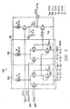
- FIG. 6 is a schematic diagram illustrating a PWM comparator 600 having a capacitive latch 402, high-speed command stage 602, high speed sense stage 604 and independent offset and threshold settings (REFC 502, REFT 606 and REFS 504) in accordance with one embodiment of the present invention.
- Voltage reference REFT 606 is the threshold of V C 308 between Current Program Mode control and Voltage Mode control.
- the prior art PWM Comparator system 300 is robust to noise, it suffers from delays that are imposed by (F1) 302. Therefore, in order for this comparator 300 to function properly for low ranges of V S 306, an offset to V G6 304 must be incorporated.
- the offset is implemented by selecting M2 to have much larger gain and drain-source admittance than M1.
- the differential amplifier 303 gain must be high in order to supply enough signal to cross the thresholds of inverter I1. High gain, as stated above, is a conflicting requirement with high speed.
- the digital nature of the PWM Comparator 300 and latch 302 also causes the output V M 322 to suddenly lose signal when V S 306 and V C 308 become small signals which will cause pulse skipping at low duty ratios.
- a PWM Comparator 600 implements the latch function in an analog circuit in contrast with prior art digital solutions. This has the benefit of low delay times and smooth transitions between modes of operations, which results in smooth operation to zero duty ratio.
- the prior art digital solution can merely operate to a minimum duty ratio, below which it hops between zero and the minimum duty ratio, thereby exhibiting erratic behavior at low duty cycle compared to the present analog solution.
- the present solution further operates faster than prior art solutions since it does not have logic and set-up delays that are associated with latches.
- the present invention presents a significant advancement in the art of PWM control technology.
- an illustrative embodiment of the present invention may comprise: a power supply PWM control system comprising, a first differential stage responsive to a voltage control signal (V C ) for generating a Voltage Mode Control signal, a second differential stage responsive to a current sense (V S ) signal for generating a Current Program Mode Control signal, and a third differential stage in communication with the first differential stage for establishing a threshold for the voltage control signal associated with the first differential stage.
- V C voltage control signal
- V S current sense
- This embodiment may include the following additional features:
- a yet further illustrative embodiment of the present invention may comprise a power supply pulse width modulation (PWM) control system comprising, a differential amplifier system having a voltage control signal (V C ) input, a current sense (V S ) signal input and a signal output, the differential amplifier system operable for generating an output signal controlled by a current sense signal and a control voltage signal, an analog latch, a latch set element operable in response to a PWM system clock signal to set the analog latch, a latch reset element operable in response to the differential amplifier system output signal to reset the analog latch and to generate an analog PWM signal therefrom; and a digital converter operable in response to the analog PWM signal to generate a digital PWM output signal therefrom.
- PWM pulse width modulation
- This embodiment may also include the following additional features:
Landscapes
- Engineering & Computer Science (AREA)
- Power Engineering (AREA)
- Dc-Dc Converters (AREA)
- Amplifiers (AREA)
- Control Of Electrical Variables (AREA)
Abstract
Description
Claims (17)
- A power supply pulse width modulation (PWM) control system comprising:a differential amplifier having a voltage control signal (VC) input, a current sense (VS) signal input and a signal output for generating an output signal proportional to a difference between a current sense signal and a control voltage signal;a capacitive PWM memory element;a PWM memory set element for charging the capacitive PWM memory element in response to a PWM system clock signal;a PWM memory discharge element for discharging the capacitive PWM memory element in response to the differential amplifier system output signal and for generating an analog PWM signal therefrom; anda digital converter for generating a digital PWM output signal in response to the differential amplifier system output signal therefrom.
- The power supply PWM control system according to claim 1, wherein the capacitive PWM memory element comprises a capacitor.
- The power supply PWM control system according to claim 1 or claim 2, wherein the PWM memory set element comprises a PMOS transistor.
- The power supply PWM control system according to any of claims 1 to 3, wherein the PWM memory discharge element is a NMOS transistor.
- The power supply PWM control system according to any preceding claim, wherein the digital converter comprises a non-inverting buffer.
- The power supply PWM control system according to any preceding claim further comprising;a current source in cascade with the PWM memory set element for transferring current to the capacitive memory element in response to each PWM system clock signal.
- The power supply PWM control system according to any preceding claim, wherein the differential amplifier is unbalanced.
- The power supply PWM control system according to any preceding claim, wherein the differential amplifier system comprises a current source, a first PMOS transistor having a source node connected to the current source, a gate node configured as the current sense signal input, and a drain; a second PMOS transistor having a source node connected to the current source, a gate node configured as the voltage control signal input, and a drain; a first NMOS transistor having a gate node, a drain node connected to its gate node and further connected to the first PMOS transistor drain node, and a source node connected to a system ground; and a second NMOS transistor having a gate node connected to the first NMOS transistor gate node, a drain node connected to the second PMOS transistor drain node, and a source node connected to the system ground.
- The power supply PWM control system according to claim 8, wherein the second PMOS transistor is configured to have more gain than the first PMOS transistor.
- The power supply PWM control system according to any preceding claim, wherein the differential amplifier system comprises a first differential stage having the voltage control signal input and an output, a second differential stage having the current sense signal input, an input in communication with the first differential stage output, and further having the differential amplifier system output, wherein the first and second differential amplifier stages are operable for generating an output signal proportional to a difference between a current sense signal and a control voltage signal.
- The power supply PWM control system according to claim 10 wherein the first differential stage comprises a first current source, a first PMOS transistor having a source node connected to the first current source, a gate node configured as the voltage control signal input and a drain connected to a system ground; a second PMOS transistor having a source node connected to the first current source, a gate node and a drain node; an NMOS transistor having a drain node connected to the second PMOS transistor drain node, a gate node connected to its drain node and a source node connected to the system ground; and a first reference capacitor connected at one end to the system ground and connected at its opposite end to the second PMOS transistor gate node, wherein the first reference capacitor is operable for establishing a first DC offset voltage.
- The power supply PWM control system according to claim 11, wherein the second differential stage comprises a second current source, a third PMOS transistor having a source node connected to the second current source, a gate node configured as the current sense signal input and a drain connected to a system ground; a fourth PMOS transistor having a source node connected to the second current source, a gate node and a drain node; a second NMOS transistor having a drain node connected to the fourth PMOS transistor drain node, a gate node connected to the second PMOS transistor drain node and a source node connected to the system ground; and a second reference capacitor connected at one end to the system ground and connected at its opposite end to the fourth PMOS transistor gate node, wherein the second reference capacitor is operational to establish a second DC offset voltage and further wherein the first DC offset voltage is associated with the second NMOS transistor and is operable for establishing its bias.
- The power supply PWM control system according to claim 12, wherein the second current source is capable of providing a larger current than that provided by the first current source.
- The power supply PWM control system according to claim 13, wherein the third and fourth PMOS transistors have a higher transconductance than that associated with the first and second PMOS transistors respectively.
- The power supply PWM control system according to claim 14 wherein the differential amplifier system further comprises a third differential stage for setting a transition voltage level where the current sense signal ceases to effect a duty ratio independent of other power supply PWM control system gains and bias currents.
- The power supply PWM control system according to any preceding claim, wherein the differential amplifier system comprises a high speed command stage, a high speed sense stage and a differential stage having a reference capable of setting a transition voltage level where the current sense signal ceases to effect a duty ratio independent of other power supply PWM control system gains and bias currents.
- The power supply PWM control system according to claim 16 further comprising:a reference capacitor operable in association with the high speed command stage, the high speed sense stage and the differential stage arranged for establishing a voltage control signal threshold between Current Program Mode and Voltage Mode Control.
Applications Claiming Priority (2)
| Application Number | Priority Date | Filing Date | Title |
|---|---|---|---|
| US684285 | 2000-10-06 | ||
| US09/684,285 US6320768B1 (en) | 2000-10-06 | 2000-10-06 | Power supply pulse width modulation (PWM) control system |
Publications (3)
| Publication Number | Publication Date |
|---|---|
| EP1199790A2 true EP1199790A2 (en) | 2002-04-24 |
| EP1199790A3 EP1199790A3 (en) | 2003-01-22 |
| EP1199790B1 EP1199790B1 (en) | 2007-08-01 |
Family
ID=24747433
Family Applications (1)
| Application Number | Title | Priority Date | Filing Date |
|---|---|---|---|
| EP01000524A Expired - Lifetime EP1199790B1 (en) | 2000-10-06 | 2001-10-08 | Power supply pulse width modulation (PWM) control system |
Country Status (6)
| Country | Link |
|---|---|
| US (1) | US6320768B1 (en) |
| EP (1) | EP1199790B1 (en) |
| JP (1) | JP2002186250A (en) |
| KR (1) | KR100889666B1 (en) |
| DE (1) | DE60129649T2 (en) |
| TW (1) | TW543268B (en) |
Families Citing this family (31)
| Publication number | Priority date | Publication date | Assignee | Title |
|---|---|---|---|---|
| US6949916B2 (en) | 2002-11-12 | 2005-09-27 | Power-One Limited | System and method for controlling a point-of-load regulator |
| US7394445B2 (en) | 2002-11-12 | 2008-07-01 | Power-One, Inc. | Digital power manager for controlling and monitoring an array of point-of-load regulators |
| US7456617B2 (en) | 2002-11-13 | 2008-11-25 | Power-One, Inc. | System for controlling and monitoring an array of point-of-load regulators by a host |
| US6833691B2 (en) | 2002-11-19 | 2004-12-21 | Power-One Limited | System and method for providing digital pulse width modulation |
| US7882372B2 (en) | 2002-12-21 | 2011-02-01 | Power-One, Inc. | Method and system for controlling and monitoring an array of point-of-load regulators |
| US7266709B2 (en) | 2002-12-21 | 2007-09-04 | Power-One, Inc. | Method and system for controlling an array of point-of-load regulators and auxiliary devices |
| US7249267B2 (en) | 2002-12-21 | 2007-07-24 | Power-One, Inc. | Method and system for communicating filter compensation coefficients for a digital power control system |
| US7673157B2 (en) | 2002-12-21 | 2010-03-02 | Power-One, Inc. | Method and system for controlling a mixed array of point-of-load regulators through a bus translator |
| US7743266B2 (en) | 2002-12-21 | 2010-06-22 | Power-One, Inc. | Method and system for optimizing filter compensation coefficients for a digital power control system |
| US7836322B2 (en) | 2002-12-21 | 2010-11-16 | Power-One, Inc. | System for controlling an array of point-of-load regulators and auxiliary devices |
| US7737961B2 (en) | 2002-12-21 | 2010-06-15 | Power-One, Inc. | Method and system for controlling and monitoring an array of point-of-load regulators |
| US7373527B2 (en) | 2002-12-23 | 2008-05-13 | Power-One, Inc. | System and method for interleaving point-of-load regulators |
| US7023190B2 (en) | 2003-02-10 | 2006-04-04 | Power-One, Inc. | ADC transfer function providing improved dynamic regulation in a switched mode power supply |
| US7710092B2 (en) | 2003-02-10 | 2010-05-04 | Power-One, Inc. | Self tracking ADC for digital power supply control systems |
| US7080265B2 (en) | 2003-03-14 | 2006-07-18 | Power-One, Inc. | Voltage set point control scheme |
| US6936999B2 (en) | 2003-03-14 | 2005-08-30 | Power-One Limited | System and method for controlling output-timing parameters of power converters |
| US7044571B2 (en) * | 2003-10-28 | 2006-05-16 | Hewlett-Packard Development Company, L.P. | Power supply adjustment |
| US7057907B2 (en) * | 2003-11-21 | 2006-06-06 | Fairchild Semiconductor Corporation | Power converter having improved control |
| US7372682B2 (en) | 2004-02-12 | 2008-05-13 | Power-One, Inc. | System and method for managing fault in a power system |
| US7554310B2 (en) | 2005-03-18 | 2009-06-30 | Power-One, Inc. | Digital double-loop output voltage regulation |
| US7141956B2 (en) | 2005-03-18 | 2006-11-28 | Power-One, Inc. | Digital output voltage regulation circuit having first control loop for high speed and second control loop for high accuracy |
| US7239115B2 (en) | 2005-04-04 | 2007-07-03 | Power-One, Inc. | Digital pulse width modulation controller with preset filter coefficients |
| US7327149B2 (en) * | 2005-05-10 | 2008-02-05 | Power-One, Inc. | Bi-directional MOS current sense circuit |
| US7515444B2 (en) * | 2005-11-01 | 2009-04-07 | Schumacher Electric Corporation | Converter with selective current mode and voltage mode controlled switching |
| US20070262801A1 (en) * | 2006-05-10 | 2007-11-15 | Technologies Ltrim Inc. | Pulse width modulation circuit and method therefor |
| US7518885B2 (en) * | 2006-10-04 | 2009-04-14 | Power Integrations, Inc. | Method and apparatus for a control circuit with multiple operation modes |
| US7834613B2 (en) | 2007-10-30 | 2010-11-16 | Power-One, Inc. | Isolated current to voltage, voltage to voltage converter |
| KR101029874B1 (en) * | 2010-08-23 | 2011-04-18 | 서울반도체 주식회사 | Ac led dimmer and dimming method thereby |
| KR20140077058A (en) * | 2012-12-13 | 2014-06-23 | 현대자동차주식회사 | Fault diagnosis system for dc-dc converter |
| US9979285B1 (en) * | 2017-10-17 | 2018-05-22 | Crane Electronics, Inc. | Radiation tolerant, analog latch peak current mode control for power converters |
| US10425080B1 (en) | 2018-11-06 | 2019-09-24 | Crane Electronics, Inc. | Magnetic peak current mode control for radiation tolerant active driven synchronous power converters |
Family Cites Families (8)
| Publication number | Priority date | Publication date | Assignee | Title |
|---|---|---|---|---|
| GB2075786B (en) * | 1980-03-21 | 1984-07-11 | Electrotech Instr Ltd | Switch mode converters |
| ATE97522T1 (en) * | 1988-09-26 | 1993-12-15 | Siemens Ag | CMOS PULSE WIDTH MODULATOR. |
| JPH09121536A (en) * | 1995-08-17 | 1997-05-06 | Harris Corp | Dual mode DC-DC converter and conversion method |
| EP0871328B1 (en) * | 1997-04-09 | 2003-08-13 | STMicroelectronics S.r.l. | Control of the output power of a dc-dc converter upon varying the switching frequency |
| US5815381A (en) * | 1997-06-06 | 1998-09-29 | Burr-Brown Corporation | Single-barrier closed loop DC-to-DC converter and method |
| JP3467679B2 (en) * | 1998-05-11 | 2003-11-17 | 株式会社豊田自動織機 | DC / DC converter |
| JP2000069746A (en) * | 1998-08-21 | 2000-03-03 | Fujitsu Ltd | Control method of DC-DC converter, control circuit of DC-DC converter, and DC-DC converter |
| US6188588B1 (en) * | 1999-10-07 | 2001-02-13 | International Business Machine Corporation | Switching controller and method for operating a flyback converter in a critically continuous conduction mode |
-
2000
- 2000-10-06 US US09/684,285 patent/US6320768B1/en not_active Expired - Lifetime
-
2001
- 2001-10-05 TW TW090124697A patent/TW543268B/en not_active IP Right Cessation
- 2001-10-05 KR KR1020010061360A patent/KR100889666B1/en not_active Expired - Fee Related
- 2001-10-05 JP JP2001309791A patent/JP2002186250A/en not_active Withdrawn
- 2001-10-08 DE DE60129649T patent/DE60129649T2/en not_active Expired - Lifetime
- 2001-10-08 EP EP01000524A patent/EP1199790B1/en not_active Expired - Lifetime
Also Published As
| Publication number | Publication date |
|---|---|
| KR100889666B1 (en) | 2009-03-19 |
| TW543268B (en) | 2003-07-21 |
| US6320768B1 (en) | 2001-11-20 |
| KR20020027258A (en) | 2002-04-13 |
| DE60129649D1 (en) | 2007-09-13 |
| EP1199790B1 (en) | 2007-08-01 |
| DE60129649T2 (en) | 2008-05-21 |
| EP1199790A3 (en) | 2003-01-22 |
| JP2002186250A (en) | 2002-06-28 |
Similar Documents
| Publication | Publication Date | Title |
|---|---|---|
| EP1199790B1 (en) | Power supply pulse width modulation (PWM) control system | |
| US6307409B1 (en) | Gate driver circuit for high and low side switches with primary and secondary shoot-through protection | |
| US10483977B1 (en) | Level shifter | |
| US12341425B2 (en) | Power converter control with programmable blanking time | |
| EP2122799A1 (en) | Wide-input windowed nonlinear analog-to-digital converter for high-frequency digitally controlled smps | |
| US4739193A (en) | Drive circuit with limited signal transition rate for RFI reduction | |
| WO2008050267A2 (en) | Power amplifier | |
| JP2004056983A (en) | Power supply circuit | |
| US12101083B2 (en) | High speed driver for high frequency DCDC converter | |
| US6822884B1 (en) | Pulse width modulated charge pump | |
| US3903431A (en) | Clocked dynamic inverter | |
| US4952863A (en) | Voltage regulator with power boost system | |
| CN101136589A (en) | Semiconductor devices, step-down chopper regulators, and electronic equipment | |
| US7102439B2 (en) | Low voltage differential amplifier circuit and a sampled low power bias control technique enabling accommodation of an increased range of input levels | |
| JP4939895B2 (en) | Level shifter circuit | |
| US12407248B2 (en) | Feedforward frequency response for resonant charge pump | |
| EP0962050B1 (en) | Output stage with self-calibrating slew rate control | |
| US6100742A (en) | Driver circuit for slope-controlled pulse switching of a load | |
| US10693423B2 (en) | Dynamic amplification circuit | |
| US4468576A (en) | Inverter circuit having transistors operable in a shallow saturation region for avoiding fluctuation of electrical characteristics | |
| US11108321B2 (en) | High-efficiency pulse width modulation for switching power converters | |
| US7479811B2 (en) | Sample/hold circuit module | |
| KR100349356B1 (en) | Power on reset circuit | |
| EP1248371A1 (en) | A converter for converting the level of differential signals | |
| US6903577B2 (en) | Delay circuit |
Legal Events
| Date | Code | Title | Description |
|---|---|---|---|
| PUAI | Public reference made under article 153(3) epc to a published international application that has entered the european phase |
Free format text: ORIGINAL CODE: 0009012 |
|
| AK | Designated contracting states |
Kind code of ref document: A2 Designated state(s): AT BE CH CY DE DK ES FI FR GB GR IE IT LI LU MC NL PT SE TR |
|
| AX | Request for extension of the european patent |
Free format text: AL;LT;LV;MK;RO;SI |
|
| PUAL | Search report despatched |
Free format text: ORIGINAL CODE: 0009013 |
|
| AK | Designated contracting states |
Kind code of ref document: A3 Designated state(s): AT BE CH CY DE DK ES FI FR GB GR IE IT LI LU MC NL PT SE TR |
|
| AX | Request for extension of the european patent |
Free format text: AL;LT;LV;MK;RO;SI |
|
| 17P | Request for examination filed |
Effective date: 20030722 |
|
| AKX | Designation fees paid |
Designated state(s): AT BE CH CY DE DK ES FI FR GB GR IE IT LI LU MC NL PT SE TR |
|
| GRAP | Despatch of communication of intention to grant a patent |
Free format text: ORIGINAL CODE: EPIDOSNIGR1 |
|
| RBV | Designated contracting states (corrected) |
Designated state(s): DE FR GB |
|
| GRAS | Grant fee paid |
Free format text: ORIGINAL CODE: EPIDOSNIGR3 |
|
| GRAA | (expected) grant |
Free format text: ORIGINAL CODE: 0009210 |
|
| AK | Designated contracting states |
Kind code of ref document: B1 Designated state(s): DE FR GB |
|
| REG | Reference to a national code |
Ref country code: GB Ref legal event code: FG4D |
|
| REF | Corresponds to: |
Ref document number: 60129649 Country of ref document: DE Date of ref document: 20070913 Kind code of ref document: P |
|
| ET | Fr: translation filed | ||
| PLBE | No opposition filed within time limit |
Free format text: ORIGINAL CODE: 0009261 |
|
| STAA | Information on the status of an ep patent application or granted ep patent |
Free format text: STATUS: NO OPPOSITION FILED WITHIN TIME LIMIT |
|
| 26N | No opposition filed |
Effective date: 20080506 |
|
| REG | Reference to a national code |
Ref country code: FR Ref legal event code: PLFP Year of fee payment: 16 |
|
| PGFP | Annual fee paid to national office [announced via postgrant information from national office to epo] |
Ref country code: GB Payment date: 20160926 Year of fee payment: 16 |
|
| PGFP | Annual fee paid to national office [announced via postgrant information from national office to epo] |
Ref country code: FR Payment date: 20160926 Year of fee payment: 16 |
|
| PGFP | Annual fee paid to national office [announced via postgrant information from national office to epo] |
Ref country code: DE Payment date: 20161031 Year of fee payment: 16 |
|
| REG | Reference to a national code |
Ref country code: DE Ref legal event code: R119 Ref document number: 60129649 Country of ref document: DE |
|
| GBPC | Gb: european patent ceased through non-payment of renewal fee |
Effective date: 20171008 |
|
| REG | Reference to a national code |
Ref country code: FR Ref legal event code: ST Effective date: 20180629 |
|
| PG25 | Lapsed in a contracting state [announced via postgrant information from national office to epo] |
Ref country code: GB Free format text: LAPSE BECAUSE OF NON-PAYMENT OF DUE FEES Effective date: 20171008 Ref country code: DE Free format text: LAPSE BECAUSE OF NON-PAYMENT OF DUE FEES Effective date: 20180501 |
|
| PG25 | Lapsed in a contracting state [announced via postgrant information from national office to epo] |
Ref country code: FR Free format text: LAPSE BECAUSE OF NON-PAYMENT OF DUE FEES Effective date: 20171031 |