EP1199742A2 - Multi-layered polysilicon gate process - Google Patents
Multi-layered polysilicon gate process Download PDFInfo
- Publication number
- EP1199742A2 EP1199742A2 EP01000537A EP01000537A EP1199742A2 EP 1199742 A2 EP1199742 A2 EP 1199742A2 EP 01000537 A EP01000537 A EP 01000537A EP 01000537 A EP01000537 A EP 01000537A EP 1199742 A2 EP1199742 A2 EP 1199742A2
- Authority
- EP
- European Patent Office
- Prior art keywords
- layer
- forming
- gate
- transistor gate
- notch
- Prior art date
- Legal status (The legal status is an assumption and is not a legal conclusion. Google has not performed a legal analysis and makes no representation as to the accuracy of the status listed.)
- Withdrawn
Links
Images

Classifications
-
- H—ELECTRICITY
- H10—SEMICONDUCTOR DEVICES; ELECTRIC SOLID-STATE DEVICES NOT OTHERWISE PROVIDED FOR
- H10D—INORGANIC ELECTRIC SEMICONDUCTOR DEVICES
- H10D64/00—Electrodes of devices having potential barriers
- H10D64/20—Electrodes characterised by their shapes, relative sizes or dispositions
- H10D64/27—Electrodes not carrying the current to be rectified, amplified, oscillated or switched, e.g. gates
- H10D64/311—Gate electrodes for field-effect devices
- H10D64/411—Gate electrodes for field-effect devices for FETs
- H10D64/511—Gate electrodes for field-effect devices for FETs for IGFETs
- H10D64/517—Gate electrodes for field-effect devices for FETs for IGFETs characterised by the conducting layers
- H10D64/518—Gate electrodes for field-effect devices for FETs for IGFETs characterised by the conducting layers characterised by their lengths or sectional shapes
-
- H—ELECTRICITY
- H10—SEMICONDUCTOR DEVICES; ELECTRIC SOLID-STATE DEVICES NOT OTHERWISE PROVIDED FOR
- H10D—INORGANIC ELECTRIC SEMICONDUCTOR DEVICES
- H10D64/00—Electrodes of devices having potential barriers
- H10D64/01—Manufacture or treatment
- H10D64/013—Manufacture or treatment of electrodes having a conductor capacitively coupled to a semiconductor by an insulator
- H10D64/01302—Manufacture or treatment of electrodes having a conductor capacitively coupled to a semiconductor by an insulator the insulator being formed after the semiconductor body, the semiconductor being silicon
- H10D64/01304—Manufacture or treatment of electrodes having a conductor capacitively coupled to a semiconductor by an insulator the insulator being formed after the semiconductor body, the semiconductor being silicon characterised by the conductor
- H10D64/01306—Manufacture or treatment of electrodes having a conductor capacitively coupled to a semiconductor by an insulator the insulator being formed after the semiconductor body, the semiconductor being silicon characterised by the conductor the conductor comprising a layer of silicon contacting the insulator, e.g. polysilicon
-
- H—ELECTRICITY
- H10—SEMICONDUCTOR DEVICES; ELECTRIC SOLID-STATE DEVICES NOT OTHERWISE PROVIDED FOR
- H10D—INORGANIC ELECTRIC SEMICONDUCTOR DEVICES
- H10D64/00—Electrodes of devices having potential barriers
- H10D64/01—Manufacture or treatment
- H10D64/013—Manufacture or treatment of electrodes having a conductor capacitively coupled to a semiconductor by an insulator
- H10D64/01302—Manufacture or treatment of electrodes having a conductor capacitively coupled to a semiconductor by an insulator the insulator being formed after the semiconductor body, the semiconductor being silicon
- H10D64/01304—Manufacture or treatment of electrodes having a conductor capacitively coupled to a semiconductor by an insulator the insulator being formed after the semiconductor body, the semiconductor being silicon characterised by the conductor
- H10D64/01324—Manufacture or treatment of electrodes having a conductor capacitively coupled to a semiconductor by an insulator the insulator being formed after the semiconductor body, the semiconductor being silicon characterised by the conductor characterised by the sectional shape, e.g. T or inverted-T
-
- H—ELECTRICITY
- H10—SEMICONDUCTOR DEVICES; ELECTRIC SOLID-STATE DEVICES NOT OTHERWISE PROVIDED FOR
- H10D—INORGANIC ELECTRIC SEMICONDUCTOR DEVICES
- H10D64/00—Electrodes of devices having potential barriers
- H10D64/01—Manufacture or treatment
- H10D64/013—Manufacture or treatment of electrodes having a conductor capacitively coupled to a semiconductor by an insulator
- H10D64/01302—Manufacture or treatment of electrodes having a conductor capacitively coupled to a semiconductor by an insulator the insulator being formed after the semiconductor body, the semiconductor being silicon
- H10D64/01304—Manufacture or treatment of electrodes having a conductor capacitively coupled to a semiconductor by an insulator the insulator being formed after the semiconductor body, the semiconductor being silicon characterised by the conductor
- H10D64/01326—Aspects related to lithography, isolation or planarisation of the conductor
Definitions
- the present invention is generally related to the field of semiconductor devices, and more specifically, to a multi-layered polysilicon process for reducing gate capacitance
- a typical MOS transistor is shown in Figure 1.
- a gate dielectric 20 is formed on a semiconductor substrate 10 and a transistor gate 30 is formed on the gate dielectric 20.
- ion implantation is used to form the drain and source extension regions 40 in the substrate 10.
- Sidewall structures 50 are then formed adjacent to the gate 30 and the source and drain regions 60 are then formed by ion implantation.
- lateral diffusion of the implanted species will result in the formation of the overlap regions 70 shown in Figure 1.
- These overlap regions 70 gives rise to "overlap capacitances".
- overlap capacitances depends on the thickness of the gate dielectric 20 in the region of overlap 70 as well as the area of the overlap region. As the area of the transistor gate 30 is reduced, this overlap capacitance becomes a larger percentage of the total overall transistor capacitance resulting in a reduction in transistor and integrated circuit performance.
- a number of different techniques are currently being used to reduce this overlap capacitance. These include the use of silicon oxide spacers between the transistor gate 30 and the sidewall structures 50 and the formation of a notch at the bottom of the transistor gate adjacent to the gate dielectric 20. The current methods used to form the notch involve timed etches which are unreliable, not easily controlled, and not very reproducible.
- the size of the transistor gate is the most critical parameter in determining transistor performance and reliability and as such any processing technique which varies the size of the transistor gate must be precisely controllable, reproducible, and reliable. There is therefore a great need for a method of forming a notch on a transistor gate that is precisely controllable, reproducible, and reliable.
- the instant invention provides a method for forming a notched gate for MOS transistors.
- the method comprises forming a multi-layered gate structure comprised of layers with differing oxidation rates.
- the oxidation rates of the various layers are varied by the incorporation of an oxidation rate retardant such as carbon and nitrogen or a species that will enhance the oxidation rate such as chlorine or fluorine.
- Thermal oxidation processes after gate etch will result in the formation of a notched gate structure.
- the notched gate method of the instant invention is precisely controllable resulting in increased uniformity compared to existing methods.
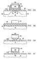
- a silicon substrate 10 which may be single-crystal silicon or an epitaxial silicon layer formed on a single crystal substrate is provided as shown in Figure 2A.
- the substrate may contain isolation structures and other semiconductor device structures which are not shown for clarity.
- a gate dielectric 20 is formed on substrate 10.
- Gate dielectric 20 may be comprised of an oxide, thermally grown SiO 2 , a nitride, an oxynitride, a silicate or any combination thereof, and is preferably on the order of 1 to 10 nm thick.
- the gate dielectric 20 can be formed using any dielectric material with suitable properties.
- first or lower silicon containing layer 130 is formed over the gate dielectric 20.
- a second or upper layer of silicon containing material 140 is formed over the first silicon containing layer 130.
- both first and second silicon containing layers 130, 140 are comprised of amorphous silicon.
- Other embodiments will include any combination of single crystal silicon, polycrystalline silicon, or amorphous silicon among the layers 130 and 140.
- nitrogen or carbon is incorporated into the second silicon containing layer 140.
- a nitrogen source gas such as N 2 O or NH 3 can be introduced during actual film deposition to incorporate nitrogen into the film 140 during growth.
- Nitrogen can also be incorporated into the second layer 140 by implanting a nitrogen containing species into the film 140 after formation.
- Carbon can be incorporated into the second layer 140 by introducing a carbon containing species during a CVD layer formation process or by implanting the second layer 140 with a carbon containing species after the layer 140 is formed. Introducing nitrogen or carbon into the second layer 140 will retard the oxidation rate of the second layer 140 compared to the first layer 130 during subsequent process steps.
- the instant invention is not intended to be limited to the use of nitrogen and carbon. Any species which retards the oxidation rate of the second layer 140 to a predetermined value can be used.
- the description of the use of nitrogen and carbon are provided by way of example only and are intended to be illustrative embodiments of the instant invention.
- the oxidation rate of the first layer 130 can be enhanced compared to that of the second layer 140 by incorporating chlorine, fluorine or bromine into the first layer 130.
- This can be accomplished by introducing species containing chlorine, fluorine, or bromine during a CVD process to form the layer 130 or by implanting these species into the layer 130 after it is formed. Any species which enhances the oxidation rate of the first layer 130 to a predetermined value can be used.
- the description of the use of chlorine, fluorine, and bromine are intended to be illustrative embodiments of the instant invention.
- Illustrated in Figure 2B is the structure of Figure 2A following an anisotropic transistor gate etch process to define the transistor gate region 150.
- the transistor gate 150 comprises a multi-layer structure comprising layers 130 and 140.
- a thermal oxidation process is performed. This oxidation process results in the formation of a silicon oxide layer 160 around the transistor gate 150 and a notch 155 in the first silicon containing layer 130.
- the formation of the notch 155 in layer 130 is due to the different oxidation rates of the layers 130 and 140. This difference in oxidation rates is due to nitrogen or carbon incorporation in the second layer 140 or fluorine, chlorine, or bromine incorporation into the first layer 130.
- the offset distance 165 between the edge of the gate and the edge of the drain and source extension implants will be controlled by the different oxidation rates of the first and second layers 130 and 140 and the oxidation process conditions. Because the oxidation rates of the layers is well known or can be easily measured and the oxidation process itself is precisely controllable.
- the notch 155 produced in the manner described in the instant invention is precisely controllable, reproducible, and reliable.
- the MOS transistor can be completed using standard semiconductor processing.
- a completed transistor is shown in Figure 2D.
- the overlap of the transistor gate 150 and the drain and source extensions 40 have been reduced by the notch 155 in the first layer 130.
- the notched transistor gate has the added advantage of reducing the transistor gate length (and capacitance) while maintaining ease of silicidation with a longer gate length at the top of the transistor gate 150.
- a dual etch process is used to form the transistor gate.
- an anisotropic etch is used to etch the second layer 140 resulting in practically parallel vertical sides.
- the endpoint of the anisotropic etch is determined by detecting the point where the nitrogen or carbon content in the etched species fall below some predetermined value.
- the endpoint of the anisotropic etch is determined by detecting a rise in the concentration of chlorine, fluorine, or bromine in the etched species.
- a more isotropic etch is used to etch the first layer 130.
- This isotropic etch results in a notched transistor gate 165 by forming an initial notch 170 in the first layer 130.
- This dual etch process is followed by thermal oxidation which oxidizes the layers at different rates resulting in an oxide layer 160 and enhancement of the notch 175 in the first layer.
- the MOS transistor can be completed using standard semiconductor processing.
Landscapes
- Insulated Gate Type Field-Effect Transistor (AREA)
- Electrodes Of Semiconductors (AREA)
- Formation Of Insulating Films (AREA)
Abstract
Description
Claims (10)
- A method of fabricating a transistor gate comprising:providing a semiconductor substrate (10) with a gate dielectric (20);forming a first layer (130) over said gate dielectric (20) with a first oxidation rate;forming a second layer (140) over said first layer (130) with a second oxidation rate such that said second oxidation rate is less that said first oxidation rate;forming a transistor gate structure (150) by etching said first and second layers (130;140); andforming a notch (155;170;175) at least in said first layer (130).
- The method of claim 1, wherein said step of forming said first layer (130) comprises forming a silicon containing layer.
- The method of claim 1 or claim 2, wherein said step of forming said second layer (140) comprises forming a silicon containing layer.
- The method of claim 2 or claim 3, wherein said step of forming said first layer (130) comprises forming a layer containing a species selected from the group consisting of fluorine, chlorine, and bromine.
- The method of claim 3 or claim 4, wherein said step of forming said second layer (140) comprises forming layer containing a species selected from the group consisting of carbon and nitrogen.
- The method of any preceding claim, wherein said step of forming said first layer (130) comprises forming a layer that comprises amorphous silicon.
- The method of any preceding claim, wherein said step of forming said second layer (140) comprises forming a layer that comprises amorphous silicon.
- The method of any preceding claim, wherein the step of forming the notch (155;170;175) comprises oxidizing said first and second layers (130;140).
- The method of claim 8, wherein said oxidizing step comprises oxidizing said first and second layers (130;140) using a thermal oxidation process.
- The method of any preceding claim, wherein the step of forming a transistor gate (150) comprises etching said second layer (140) with an anisotropic process to define the top layer of said transistor gate (150), and wherein the step of forming a notch comprises etching said first layer (130) with an isotropic process.
Applications Claiming Priority (2)
| Application Number | Priority Date | Filing Date | Title |
|---|---|---|---|
| US24157100P | 2000-10-19 | 2000-10-19 | |
| US241571P | 2000-10-19 |
Publications (2)
| Publication Number | Publication Date |
|---|---|
| EP1199742A2 true EP1199742A2 (en) | 2002-04-24 |
| EP1199742A3 EP1199742A3 (en) | 2002-10-09 |
Family
ID=22911237
Family Applications (1)
| Application Number | Title | Priority Date | Filing Date |
|---|---|---|---|
| EP01000537A Withdrawn EP1199742A3 (en) | 2000-10-19 | 2001-10-12 | Multi-layered polysilicon gate process |
Country Status (3)
| Country | Link |
|---|---|
| US (1) | US6645840B2 (en) |
| EP (1) | EP1199742A3 (en) |
| JP (1) | JP3877569B2 (en) |
Families Citing this family (28)
| Publication number | Priority date | Publication date | Assignee | Title |
|---|---|---|---|---|
| JP3890254B2 (en) * | 2002-05-07 | 2007-03-07 | 沖電気工業株式会社 | Manufacturing method of semiconductor device |
| US20040018647A1 (en) * | 2002-07-02 | 2004-01-29 | Applied Materials, Inc. | Method for controlling the extent of notch or undercut in an etched profile using optical reflectometry |
| US6806517B2 (en) * | 2003-03-17 | 2004-10-19 | Samsung Electronics Co., Ltd. | Flash memory having local SONOS structure using notched gate and manufacturing method thereof |
| US6905976B2 (en) * | 2003-05-06 | 2005-06-14 | International Business Machines Corporation | Structure and method of forming a notched gate field effect transistor |
| US6909151B2 (en) | 2003-06-27 | 2005-06-21 | Intel Corporation | Nonplanar device with stress incorporation layer and method of fabrication |
| US7456476B2 (en) * | 2003-06-27 | 2008-11-25 | Intel Corporation | Nonplanar semiconductor device with partially or fully wrapped around gate electrode and methods of fabrication |
| US7199011B2 (en) * | 2003-07-16 | 2007-04-03 | Texas Instruments Incorporated | Method to reduce transistor gate to source/drain overlap capacitance by incorporation of carbon |
| KR100597459B1 (en) * | 2003-12-31 | 2006-07-05 | 동부일렉트로닉스 주식회사 | Gate electrode formation method of semiconductor device |
| KR100557531B1 (en) * | 2004-03-11 | 2006-03-03 | 주식회사 하이닉스반도체 | Semiconductor device and manufacturing method thereof |
| US7105430B2 (en) * | 2004-03-26 | 2006-09-12 | Freescale Semiconductor, Inc. | Method for forming a semiconductor device having a notched control electrode and structure thereof |
| US7154118B2 (en) | 2004-03-31 | 2006-12-26 | Intel Corporation | Bulk non-planar transistor having strained enhanced mobility and methods of fabrication |
| US7042009B2 (en) | 2004-06-30 | 2006-05-09 | Intel Corporation | High mobility tri-gate devices and methods of fabrication |
| US7348284B2 (en) * | 2004-08-10 | 2008-03-25 | Intel Corporation | Non-planar pMOS structure with a strained channel region and an integrated strained CMOS flow |
| US7422946B2 (en) | 2004-09-29 | 2008-09-09 | Intel Corporation | Independently accessed double-gate and tri-gate transistors in same process flow |
| US7361958B2 (en) * | 2004-09-30 | 2008-04-22 | Intel Corporation | Nonplanar transistors with metal gate electrodes |
| US20060086977A1 (en) | 2004-10-25 | 2006-04-27 | Uday Shah | Nonplanar device with thinned lower body portion and method of fabrication |
| US7518196B2 (en) | 2005-02-23 | 2009-04-14 | Intel Corporation | Field effect transistor with narrow bandgap source and drain regions and method of fabrication |
| US20060202266A1 (en) | 2005-03-14 | 2006-09-14 | Marko Radosavljevic | Field effect transistor with metal source/drain regions |
| US7858481B2 (en) | 2005-06-15 | 2010-12-28 | Intel Corporation | Method for fabricating transistor with thinned channel |
| US7547637B2 (en) | 2005-06-21 | 2009-06-16 | Intel Corporation | Methods for patterning a semiconductor film |
| US7279375B2 (en) | 2005-06-30 | 2007-10-09 | Intel Corporation | Block contact architectures for nanoscale channel transistors |
| US7402875B2 (en) | 2005-08-17 | 2008-07-22 | Intel Corporation | Lateral undercut of metal gate in SOI device |
| US20070090416A1 (en) * | 2005-09-28 | 2007-04-26 | Doyle Brian S | CMOS devices with a single work function gate electrode and method of fabrication |
| US7485503B2 (en) | 2005-11-30 | 2009-02-03 | Intel Corporation | Dielectric interface for group III-V semiconductor device |
| US8143646B2 (en) | 2006-08-02 | 2012-03-27 | Intel Corporation | Stacking fault and twin blocking barrier for integrating III-V on Si |
| JP5171363B2 (en) * | 2008-04-08 | 2013-03-27 | 三菱電機株式会社 | Manufacturing method of semiconductor device |
| US8343824B2 (en) * | 2008-04-29 | 2013-01-01 | International Rectifier Corporation | Gallium nitride material processing and related device structures |
| US8362566B2 (en) | 2008-06-23 | 2013-01-29 | Intel Corporation | Stress in trigate devices using complimentary gate fill materials |
Family Cites Families (14)
| Publication number | Priority date | Publication date | Assignee | Title |
|---|---|---|---|---|
| KR970003903B1 (en) * | 1987-04-24 | 1997-03-22 | Hitachi Mfg Kk | Semiconductor device and fabricating method thereof |
| US4847213A (en) * | 1988-09-12 | 1989-07-11 | Motorola, Inc. | Process for providing isolation between CMOS devices |
| US5306655A (en) * | 1990-07-24 | 1994-04-26 | Matsushita Electric Industrial Co., Ltd. | Structure and method of manufacture for MOS field effect transistor having lightly doped drain and source diffusion regions |
| US5264396A (en) | 1993-01-14 | 1993-11-23 | Micron Semiconductor, Inc. | Method for enhancing nitridation and oxidation growth by introducing pulsed NF3 |
| US5580816A (en) * | 1995-06-07 | 1996-12-03 | Harris Corporation | Local oxidation process for high field threshold applications |
| JP3688816B2 (en) * | 1996-07-16 | 2005-08-31 | 株式会社東芝 | Manufacturing method of semiconductor device |
| US5891798A (en) * | 1996-12-20 | 1999-04-06 | Intel Corporation | Method for forming a High dielectric constant insulator in the fabrication of an integrated circuit |
| JPH10326891A (en) * | 1997-05-26 | 1998-12-08 | Mitsubishi Electric Corp | Semiconductor device and manufacturing method thereof |
| US5963817A (en) * | 1997-10-16 | 1999-10-05 | International Business Machines Corporation | Bulk and strained silicon on insulator using local selective oxidation |
| US6114230A (en) | 1997-12-18 | 2000-09-05 | Advanced Micro Devices, Inc. | Nitrogen ion implanted amorphous silicon to produce oxidation resistant and finer grain polysilicon based floating gates |
| US6259131B1 (en) * | 1998-05-27 | 2001-07-10 | Taiwan Semiconductor Manufacturing Company | Poly tip and self aligned source for split-gate flash cell |
| KR100318459B1 (en) * | 1998-12-22 | 2002-02-19 | 박종섭 | A method for forming titanium polycide gate electrode |
| US6335262B1 (en) * | 1999-01-14 | 2002-01-01 | International Business Machines Corporation | Method for fabricating different gate oxide thicknesses within the same chip |
| US6399469B1 (en) * | 2000-07-10 | 2002-06-04 | Advanced Micro Devices, Inc. | Fabrication of a notched gate structure for a field effect transistor using a single patterning and etch process |
-
2001
- 2001-09-28 US US09/967,061 patent/US6645840B2/en not_active Expired - Lifetime
- 2001-10-12 EP EP01000537A patent/EP1199742A3/en not_active Withdrawn
- 2001-10-19 JP JP2001322163A patent/JP3877569B2/en not_active Expired - Fee Related
Also Published As
| Publication number | Publication date |
|---|---|
| JP3877569B2 (en) | 2007-02-07 |
| EP1199742A3 (en) | 2002-10-09 |
| US20020048918A1 (en) | 2002-04-25 |
| JP2002184983A (en) | 2002-06-28 |
| US6645840B2 (en) | 2003-11-11 |
Similar Documents
| Publication | Publication Date | Title |
|---|---|---|
| US6645840B2 (en) | Multi-layered polysilicon process | |
| US6100558A (en) | Semiconductor device having enhanced gate capacitance by using both high and low dielectric materials | |
| US7622770B2 (en) | Semiconductor device having a trench gate and method of fabricating the same | |
| US6503833B1 (en) | Self-aligned silicide (salicide) process for strained silicon MOSFET ON SiGe and structure formed thereby | |
| US6136674A (en) | Mosfet with gate plug using differential oxide growth | |
| US8013397B2 (en) | Embedded stressed nitride liners for CMOS performance improvement | |
| US6900092B2 (en) | Surface engineering to prevent epi growth on gate poly during selective epi processing | |
| JP2000091578A (en) | Vertical transistor fabrication process | |
| EP1433196A2 (en) | United method and apparatus to prevent lateral oxidation in a transistor utilizing an ultra thin oxygen-diffusion barrier | |
| US20020063299A1 (en) | Semiconductor device and manufacturing method | |
| EP1456877B1 (en) | Method for composite spacer liner for improved transistor performance | |
| TWI377625B (en) | Method of semiconductor fabrication incoprorating disposable spacer into elevated source/drain processing | |
| US7544576B2 (en) | Diffusion barrier for nickel silicides in a semiconductor fabrication process | |
| JP2000022139A (en) | Semiconductor device and manufacturing method thereof | |
| US6667204B2 (en) | Semiconductor device and method of forming the same | |
| US6624486B2 (en) | Method for low topography semiconductor device formation | |
| US6323112B1 (en) | Method of fabricating integrated circuits | |
| JPH06216120A (en) | Method for forming electrically isolated structure of integrated circuit | |
| US7186632B2 (en) | Method of fabricating a semiconductor device having a decreased concentration of phosphorus impurities in polysilicon | |
| US6087248A (en) | Method of forming a transistor having thin doped semiconductor gate | |
| US20030015758A1 (en) | Semiconductor device and method therefor | |
| US20050260805A1 (en) | Semiconductor device and method for producing the same | |
| EP2276062B1 (en) | Method of etching nickel silicide and cobalt silicide and method of forming conductive lines | |
| JP2005517285A (en) | Semiconductor device including thin oxide liner and method of manufacturing the same | |
| JP2002118262A (en) | Semiconductor device and manufacturing method thereof |
Legal Events
| Date | Code | Title | Description |
|---|---|---|---|
| PUAI | Public reference made under article 153(3) epc to a published international application that has entered the european phase |
Free format text: ORIGINAL CODE: 0009012 |
|
| AK | Designated contracting states |
Kind code of ref document: A2 Designated state(s): AT BE CH CY DE DK ES FI FR GB GR IE IT LI LU MC NL PT SE TR |
|
| AX | Request for extension of the european patent |
Free format text: AL;LT;LV;MK;RO;SI |
|
| RIC1 | Information provided on ipc code assigned before grant |
Free format text: 7H 01L 21/28 A, 7H 01L 21/336 B, 7H 01L 29/423 B, 7H 01L 21/762 B |
|
| PUAL | Search report despatched |
Free format text: ORIGINAL CODE: 0009013 |
|
| AK | Designated contracting states |
Kind code of ref document: A3 Designated state(s): AT BE CH CY DE DK ES FI FR GB GR IE IT LI LU MC NL PT SE TR |
|
| AX | Request for extension of the european patent |
Free format text: AL;LT;LV;MK;RO;SI |
|
| 17P | Request for examination filed |
Effective date: 20030409 |
|
| AKX | Designation fees paid |
Designated state(s): AT BE CH CY DE DK ES FI FR GB GR IE IT LI LU MC NL PT SE TR |
|
| RBV | Designated contracting states (corrected) |
Designated state(s): DE FR GB |
|
| 17Q | First examination report despatched |
Effective date: 20040127 |
|
| STAA | Information on the status of an ep patent application or granted ep patent |
Free format text: STATUS: THE APPLICATION IS DEEMED TO BE WITHDRAWN |
|
| 18D | Application deemed to be withdrawn |
Effective date: 20050906 |