EP1199180A1 - Optical writing head comprising self-scanning light-emitting element array - Google Patents
Optical writing head comprising self-scanning light-emitting element array Download PDFInfo
- Publication number
- EP1199180A1 EP1199180A1 EP00985870A EP00985870A EP1199180A1 EP 1199180 A1 EP1199180 A1 EP 1199180A1 EP 00985870 A EP00985870 A EP 00985870A EP 00985870 A EP00985870 A EP 00985870A EP 1199180 A1 EP1199180 A1 EP 1199180A1
- Authority
- EP
- European Patent Office
- Prior art keywords
- light
- control electrode
- element array
- chips
- elements
- Prior art date
- Legal status (The legal status is an assumption and is not a legal conclusion. Google has not performed a legal analysis and makes no representation as to the accuracy of the status listed.)
- Withdrawn
Links
- 230000003287 optical effect Effects 0.000 title claims abstract description 69
- 230000003247 decreasing effect Effects 0.000 abstract description 8
- 101710129448 Glucose-6-phosphate isomerase 2 Proteins 0.000 abstract 1
- 238000010586 diagram Methods 0.000 description 8
- 238000006243 chemical reaction Methods 0.000 description 3
- 238000009792 diffusion process Methods 0.000 description 2
- 230000005855 radiation Effects 0.000 description 2
- 239000000758 substrate Substances 0.000 description 2
- 208000032365 Electromagnetic interference Diseases 0.000 description 1
- 229910001218 Gallium arsenide Inorganic materials 0.000 description 1
- 230000020169 heat generation Effects 0.000 description 1
- 238000004519 manufacturing process Methods 0.000 description 1
Images







Classifications
-
- B—PERFORMING OPERATIONS; TRANSPORTING
- B41—PRINTING; LINING MACHINES; TYPEWRITERS; STAMPS
- B41J—TYPEWRITERS; SELECTIVE PRINTING MECHANISMS, i.e. MECHANISMS PRINTING OTHERWISE THAN FROM A FORME; CORRECTION OF TYPOGRAPHICAL ERRORS
- B41J2/00—Typewriters or selective printing mechanisms characterised by the printing or marking process for which they are designed
- B41J2/435—Typewriters or selective printing mechanisms characterised by the printing or marking process for which they are designed characterised by selective application of radiation to a printing material or impression-transfer material
- B41J2/447—Typewriters or selective printing mechanisms characterised by the printing or marking process for which they are designed characterised by selective application of radiation to a printing material or impression-transfer material using arrays of radiation sources
- B41J2/45—Typewriters or selective printing mechanisms characterised by the printing or marking process for which they are designed characterised by selective application of radiation to a printing material or impression-transfer material using arrays of radiation sources using light-emitting diode [LED] or laser arrays
-
- B—PERFORMING OPERATIONS; TRANSPORTING
- B41—PRINTING; LINING MACHINES; TYPEWRITERS; STAMPS
- B41J—TYPEWRITERS; SELECTIVE PRINTING MECHANISMS, i.e. MECHANISMS PRINTING OTHERWISE THAN FROM A FORME; CORRECTION OF TYPOGRAPHICAL ERRORS
- B41J2/00—Typewriters or selective printing mechanisms characterised by the printing or marking process for which they are designed
- B41J2/435—Typewriters or selective printing mechanisms characterised by the printing or marking process for which they are designed characterised by selective application of radiation to a printing material or impression-transfer material
- B41J2/44—Typewriters or selective printing mechanisms characterised by the printing or marking process for which they are designed characterised by selective application of radiation to a printing material or impression-transfer material using single radiation source per colour, e.g. lighting beams or shutter arrangements
-
- B—PERFORMING OPERATIONS; TRANSPORTING
- B41—PRINTING; LINING MACHINES; TYPEWRITERS; STAMPS
- B41J—TYPEWRITERS; SELECTIVE PRINTING MECHANISMS, i.e. MECHANISMS PRINTING OTHERWISE THAN FROM A FORME; CORRECTION OF TYPOGRAPHICAL ERRORS
- B41J2/00—Typewriters or selective printing mechanisms characterised by the printing or marking process for which they are designed
- B41J2/435—Typewriters or selective printing mechanisms characterised by the printing or marking process for which they are designed characterised by selective application of radiation to a printing material or impression-transfer material
- B41J2/447—Typewriters or selective printing mechanisms characterised by the printing or marking process for which they are designed characterised by selective application of radiation to a printing material or impression-transfer material using arrays of radiation sources
- B41J2/455—Typewriters or selective printing mechanisms characterised by the printing or marking process for which they are designed characterised by selective application of radiation to a printing material or impression-transfer material using arrays of radiation sources using laser arrays, the laser array being smaller than the medium to be recorded
-
- H—ELECTRICITY
- H04—ELECTRIC COMMUNICATION TECHNIQUE
- H04N—PICTORIAL COMMUNICATION, e.g. TELEVISION
- H04N1/00—Scanning, transmission or reproduction of documents or the like, e.g. facsimile transmission; Details thereof
- H04N1/024—Details of scanning heads ; Means for illuminating the original
- H04N1/032—Details of scanning heads ; Means for illuminating the original for picture information reproduction
- H04N1/036—Details of scanning heads ; Means for illuminating the original for picture information reproduction for optical reproduction
-
- B—PERFORMING OPERATIONS; TRANSPORTING
- B41—PRINTING; LINING MACHINES; TYPEWRITERS; STAMPS
- B41J—TYPEWRITERS; SELECTIVE PRINTING MECHANISMS, i.e. MECHANISMS PRINTING OTHERWISE THAN FROM A FORME; CORRECTION OF TYPOGRAPHICAL ERRORS
- B41J2/00—Typewriters or selective printing mechanisms characterised by the printing or marking process for which they are designed
- B41J2/435—Typewriters or selective printing mechanisms characterised by the printing or marking process for which they are designed characterised by selective application of radiation to a printing material or impression-transfer material
- B41J2/447—Typewriters or selective printing mechanisms characterised by the printing or marking process for which they are designed characterised by selective application of radiation to a printing material or impression-transfer material using arrays of radiation sources
- B41J2/45—Typewriters or selective printing mechanisms characterised by the printing or marking process for which they are designed characterised by selective application of radiation to a printing material or impression-transfer material using arrays of radiation sources using light-emitting diode [LED] or laser arrays
- B41J2002/453—Typewriters or selective printing mechanisms characterised by the printing or marking process for which they are designed characterised by selective application of radiation to a printing material or impression-transfer material using arrays of radiation sources using light-emitting diode [LED] or laser arrays self-scanning
Definitions
- the present invention relates to an optical writing head, particularly to an optical writing head using a self-scanning light-emitting element array.
- a light printer head i.e. an optical writing head comprises a light-emitting element array in which a plurality of light-emitting elements are arrayed in one line.
- an optical writing head is structured by using a light-emitting diode (LED) array, for example, as a light-emitting element array, about 7200 LEDs are arrayed in one line for an optical writing head of 600 dpi (dots per inch) which prints on an A3 size paper.
- an electrode of each LED is electrically connected to an electrode of a driving IC.
- a wire bonding is usually used for such electrical connection.
- An IC for driving n LEDs generally converts n serial data into n parallel data, thereby controlling the light emission condition of the n LEDs.
- the number of signal lines derived from the optical writing head is equal to that of the driving ICs except the signal lines for power supply and timing.
- a particular driving IC is provided for distributing (serial-parallel conversion) data to m driving ICs so that the number of signal lines may be decreased by a factor of m.
- the conventional optical writing head has lines the number thereof is equal to that of LEDs, it is difficult to interface with an external part otherwise the number of lines to be derived is decreased by serial-parallel conversion with the particular driving IC.
- the particular driving IC is mounted on the same substrate on which the LED array is mounted, then this causes the problem in that the width of the head, i.e. the width in a direction perpendicular to the direction of LED arrangement becomes large.
- the particular driving IC for serial-parallel conversion is to be provided in the head, resulting in a high production cost.
- the inventors of the present invention have interested in a three-terminal light-emitting thyristor having a PNPN-structure as an elements of the light-emitting element array, and have already filed several patent applications (see Japanese Patent Publication Nos. 1-238962, 2-14584, 2-92650, and 2-92651.) These patent publications have disclosed that a self-scanning function for light-emitting elements may be implemented, and further have disclosed that such self-scanning light-emitting element array has a simple and compact structure for the light source of a printer, and has smaller arranging pitch of thyristors.
- the inventors have further provided a self-scanning light-emitting elelment array having such structure that an array of light-emitting thyristors having transfer function as a shift register is separated from an array of light-emitting thyristor having writable function (see Japanese Patent Publication No.2-263668.)
- the object of the present invention is to provide an optical writing head in which the number of bus lines to be derived may be decreased by using a self-scanning light-emitting element array.
- One point light-emitting type of self-scanning light-emitting element array chip used in an optical writing head comprises the following basic structure.
- the one point light-emitting type of self-scanning light-emitting element array chip comprises ;
- a plurality of chips described above are linearly arranged, a start pulse bus line is commonly connected to the respective chips, n-phases clock pulse bus lines are commonly connected to the respective chips, and write signal bus lines are separately connected to the respective chips.
- current limiting resistors to be connected to the start pulse bus line, n-phase clock pulse bus lines, and write signal bus lines are included in the chip, in the optical head of the first aspect.
- current limiting resistors to be connected to the n-phase clock pulse bus lines are included in the chip, in the optical writing head of the first aspect.
- a buffer IC is inserted in each of the n-phase clock pulse bus lines, in the optical head of the third aspect.
- a two point light-emitting type of self-scanning light-emitting element array chip is used.
- a start pulse bus line is commonly connected to the respective chips
- n-phases clock pulse bus lines are commonly connected to the respective chips
- two write signal bus lines are separately connected to the respective chips
- the two write signal bus lines are alternately connected to the light-emitting elements in each chip.
- a plural light-emitting type of self-scanning light-emitting element array chip is used.
- the plural light-emitting type of self-scanning light-emitting element array chip comprises ;
- start pulse bus line are separately connected to the respective chips
- n-phases clock pulse bus lines are commonly connected to the respective chips
- a write signal bus line is commonly connected to the respective chips.
- m is an integer ⁇ 2
- start pulse bus line are repeatedly connected to the respective chips
- n-phases clock pulse bus lines are commonly connected to the respective chips
- write signal bus lines are separately connected to every m chip neighbored to each other
- current limiting resistors to be connected to the start pulse bus line, n-phase clock pulse bus lines, and write signal bus lines are included in the chip.
- the plurality of chips are divided into groups each thereof including m (m is an integer ⁇ 2) chips, an end bonding pad of one chip is connected to the start pulse bonding of next chip in one group of chips, a start pulse bus line is commonly connected to a first chip of the respective groups, n-phase clock pulse bus lines are commonly connected to the respective chips, and write signal bus lines are separately connected to all the chips of the respective groups.
- start pulse bus lines are separately connected to every m (m is an integer ⁇ 2) chips neighbored to each other, one-phase m clock pulse bus lines are repeatedly connected to the m chips neighbored to each other, another-phase clock pulse bus lines are commonly connected to the respective chips, and a write signal bus line is commonly connected to the respective chips.
- the self-scanning light-emitting element array employs a three-terminal light-emitting thyristor.
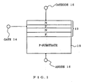
- the fundamental structure of the three-terminal light-emitting thyristor is shown in Fig.1, in which a PNPN-structure 12 is formed on a P-type GaAs substrate 10, as an example.
- a gate 14 of the thyristor serves to control a turn on-voltage.
- the turn on-voltage supplied to a cathode 16 is equal to the gate voltage + a diffusion potential of PN junction.
- the gate voltage becomes substantially equal to the anode voltage after the thyristor is turned on. Therefore, if the anode 18 is grounded, then the gate voltage becomes 0 volts.
- This self-scanning light-emitting element array comprises an array of transfer elements T 1 , T 2 , T 3 , ⁇ and an array of writable light-emitting elements L 1 , L 2 , L 3 , ⁇ , these transfer and light-emitting elements consisting of three-terminal light-emitting thyristors.
- the gate electrodes of neighboring transfer elements are connected to each other via diodes D 1 , D 2 , D 3 , ⁇ , respectively.
- Clock pulses ⁇ 1 and ⁇ 2 are alternately applied to the cathode electrodes of the transfer elements.
- V GA is a power supply (normally -5 volts), and is connected to all the gate electrodes G 1 , G 2 , G 3 , ⁇ of the transfer elements via a load resistor R L , respectively.
- a shift register is consisted by the transfer elements T 1 , T 2 , T 3 , ⁇ , the diodes D 1 , D 2 , D 3 , ⁇ , and the load resistors R L .
- Respective gate electrodes are correspondingly connected to the gate electrodes of the light-emitting elements.
- a start pulse ⁇ S is applied to the gate electrode of the first transfer element T 1
- a write signal ⁇ I is applied to all the cathode electrodes of the light-emitting elements.
- this self-scanning light-emitting array will now be described briefly. Assuming that the transfer element T 2 is in on-state, the voltage of the gate electrode G 2 is increased more than the power supply voltage V GA (-5 volts) and is driven to about 0 volts. Therefore, if the voltage of the write signal ⁇ I is lower than the diffusion voltage (about 1 volt) of PN junction, the light-emitting element L 2 may be turned into an on-state (i.e., a light-emitting state).
- the voltage of the gate electrode G 1 is about -5 volts, and the voltage of the gate electrode G 3 is about -1 volt. Consequently, the write voltage of the light-emitting element L 1 is about -6 volts, and the write voltage of the light-emitting element L 3 is about -2 volts. It is recognized from this that the voltage of the write signal ⁇ I which can write into only the light-emitting element L 2 is in a range of about -1 - -2 volts. When the light-emitting element L 2 is turned on, i.e., in the light-emitting state, the voltage of the write signal ⁇ I is cramped to -1 volt. Therefore, there is no possibility that another light-emitting element is selected and turned on.
- the amount of light emitted from the element is determined by a current due to the write signal ⁇ I . Accordingly, the light-emitting elements may emit light at any desired amount of light. In order to transfer on-state to the next element, it is necessary to turn off the element in on-state by temporarily dropping the voltage of the write signal ⁇ I down to zero volts.
- the self-scanning light-emitting element array described above When the self-scanning light-emitting element array described above is applied to an optical printer and the like, a predetermined number of transfer elements and light-emitting elements are integrated into one chip to fabricate a self-scanning light-emitting element array chip. A plurality of the self-scanning light-emitting element array chips are arrayed in one line to make a self-scanning light-emitting element array of a predetermined size.
- an optical writing head for A3 size paper is structured by arranging 56 self-scanning light-emitting element array (abbreviated as SLED) chips, each thereof is 600 dpi/128 light-emitting points/one point light-emitting type (only one light-emitting element is lighted up per chip at one time).
- SLED self-scanning light-emitting element array
- the SLED chip shown in Fig.4B comprises 128 transfer elements T 1 - T 128 and 128 writable light-emitting elements.
- the part of a shift register uses diodes for connecting gate electrodes of adjacent trasnfer elements.
- V GA denotes power supply which is connected to all the gate electrode of the transfer elements via respective load resistors R L .
- Each gate electrode of the transfer elements is also connected to a gate electrode of corresponding light-emitting element.
- a start pulse ⁇ S is applied to the gate electrode of the transfer element T 1
- transfer clock pulse ⁇ 1 and ⁇ 2 are alternately applied to the cathode electrodes of the transfer elements
- a write signal ⁇ I is applied to all the cathode electrodes of the light-emitting elements.
- the SLED chip comprises bonding pads 30, 32, 34, 36, 38 for signals ⁇ 1, ⁇ 2, V GA , ⁇ S , ⁇ I as shown in Fig.4A.
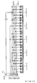
- a signal wiring to a self-scanning light-emitting element array will be described, which is structured by arranging 56 SLEDs (SLED1 - SLED56) each having bonding pads 30, 32, 34, 36, 38 described above.
- Bus lines 22, 24, 26, 28 are elongated respectively from V GA , ⁇ 2, ⁇ 1, ⁇ S terminals of a connector 20.
- the ⁇ 1 bonding pad 30 of each SLED chip is connected to the ⁇ 1 bus line 26 via a current limiting resistor R1 provided outside the chips, and the ⁇ 2 bonding pad 32 is connected to the ⁇ 2 bus line 24 via a current limiting resistor R2 provided outside the chips.
- ⁇ S bonding pad 36 is connected to the ⁇ S bus line 28 via a current limiting resistor R S provided outside the chip, and the V GA bonding pad 34 is directly connected to the V GA bus line 22.
- Each ⁇ I bonding pad of the SLED chips is connected to corresponding one of ⁇ I (1) - ⁇ I (56) terminals of the connector 20, via a current limiting resistor R I provided outside the chips through corresponding bus lines for write signals ⁇ I (1) - ⁇ I (56).
- respective SLED chips starts their transfer operation at the same time since the same start pulse ⁇ s is given to all the SLED chips.
- the amount of light emitted from one light-emitting element of each SLED chip is determined by the signals ⁇ I (1) - ⁇ I (56) applied thereto, respectively.
- This embodiment is directed to an optical writing head having current limiting resistors R1, R2, R S , R I provide within respective SLED chips, while these resistors are provided outside SLED chips in the optical writing head in Fig.3
- each SLED chip being 600 dpi/128 light-emitting points/one point light-emitting type SLED chip and including the resistors therein.
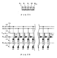
- the SLED chip used in this embodiment is shown in Figs. 6A and 6B.
- the SLED chip includes the current limiting resistors R1, R2, R S , R I as shown in Fig.6B. These resistors are inserted in ⁇ 1 line 40, ⁇ 2 line 42, ⁇ S line 46, ⁇ I line 48, respectively.
- the number of bonding pads of one chip is equal to that of the embodiment 1.
- This embodiment uses SLED chips each including current limiting resistors R1 and R2 only in place of SLED chips of the embodiment 2a.
- the SLED chip used in this embodiment is shown in Fig.7.
- the SLED chip comprises the resistors R1 and R2 inserted in the ⁇ 1 line 40 and ⁇ 2 line 42, and no resistors are inserted in the ⁇ S line 46 and ⁇ I line 48.
- the ⁇ I (1) - ⁇ I (56) terminals of the connector 20 are driven by current sources, as no resistor is inserted in the ⁇ I line 48.
- the voltage between anode and cathode of a thyristor in on-state is held equal to the foward voltage of PN junction. Utilizing this characteristic, a current source comprising the combination of a voltage source and resistor may be used.
- FIG.8 there is shown an optical writing head of this embodiment.
- buffer ICs 61 and 62 are inserted in ⁇ 1 and ⁇ 2 bus lines, respectively, of the optical writing head in the embodiment 2b.
- buffer ICs As buffer ICs are inserted in the bus lines, a higher or lower voltage than the threshold voltage may be applied to the ⁇ 1 and ⁇ 2 terminals of the connector 20. It is generally difficult for the SLED chip having transfer elements connected by a diode therebetween to operate by a 3V power supply. However, by inserting buffer ICs as described above, it may be possible to operate the SLED chip by 3V system signals, though a 5V power supply is required. As a power supply voltage is decreased in this manner, the consumption of power supply may be reduced.
- This embodiment is directed to an optical writing head for A3 size paper structured by arranging 56 SLED chips, each thereof is 600 dpi/128 light-emitting points/two points light-emitting type (two light-emitting elements are lighted up per chip at the same time), which includes resistors therein.
- Fig.9 shows the structure of the optical writing head
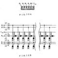
- Figs.10A and 10B show a SLED chip used in this embodiment.
- the SLED chip shown in Figs.10A and 10B further includes a writing signal ⁇ J in addition to the writing signals ⁇ I in the SLED chip in Fig.6.
- a current limiting resistor R J is inserted in ⁇ J line 49.
- the writing signals ⁇ I and ⁇ J are alternately applied to the light-emitting elements, thereby allowing two light-emitting element in one chip to light up at the same time. As a result, a duty ratio of the writing signal becomes large to increase an effective amount of emitted light.
- two writing signal bus lines, ⁇ I (1) - ⁇ I (56) and ⁇ J (1) - ⁇ J (56) bus lines are provided with every chip, so that 56 bus lines are increased as compared with the embodiment 1 and the total number of bus lines derived from the chips is 117.
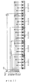
- This embodiment is directed to an optical writing head for A3 size paper structured by arranging 56 SLED chips, each thereof is 600 dpi/128 light-emitting points/plural points light-emitting type (a plurality of light-emitting elements are lighted up per chip at the same time).
- Fig.11 shows the structure of the optical writing head
- Fig.12 shows a SLED chip used in this embodiment.
- each cathode electrode of transfer elements T is alternately connected to the ⁇ 1 and ⁇ 2 lines 40, 42 via current limiting resistors 71, 72, respectively.
- Each cathode electrode of the light-emitting elements L is connected to the ⁇ I line 48 via a current limiting resistor 74.
- These resistors 71, 72, 73 are integrated in the chip.
- Each gate electrode of light-emitting elements L is connected to the gate electrode of the corresponding transfer elements T to which the clock pulse ⁇ 1 is applied.
- phase clock pulses may be used, and also more than two ⁇ s lines may be provided.
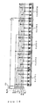
- ⁇ S (1) bus line 28(1) and ⁇ S (2) bus line 28(2) are provided as compared with the head of the embodiment 2a as shown in Fig.5.
- the ⁇ S (1) bus line 28(1) is connected to the SLED 1
- ⁇ S (2) bus line 28(2) is connected to the SLED2, SLED4, ⁇ , as shown in Fig.13.
- the number of writing signal ⁇ I is decreased by half, i.e., ⁇ I (1) - ⁇ I (28) as compared with the head as shown in Fig.5 to apply the same writing signal to every adjacent two SLED chips.
- the total number of bus lines derived from the chips is 34, i.e., the bus lines for ⁇ S (1), ⁇ S (2), ⁇ 1, ⁇ 2, V GA , ⁇ I (1) - ⁇ I (28) in addition to a ground bus line (not shown).
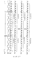
- Fig.14 shows the waveforms of the signals in the head of Fig.13. It is recognized from the figure that the start pulse ⁇ s (1) is applied to odd numbered SLED chips, the start pulse ⁇ s (2) is applied to even numbered SLED chips, and the writing signals ⁇ I (1), ⁇ I (2), ⁇ I (3), ⁇ are applied to every adjacent two SLED chips, respectively.
- phase clock pulses may be used, and also more than two ⁇ S lines may be provided.
- a chip is used in which the cathode of the final connecting diode in the SLED chip (as shown in Fig.5) of the embodiment 2a is derived as an end bonding pad ( ⁇ end ) 37.
- the ⁇ end bonding pad 37 of (2N-1)th SLED chip is connected to the ⁇ S bonding pad 36 of 2Nth SLED chip.
- the start pulse ⁇ S is applied to (2N-1)th SLED chip.
- two SLED chips may be treated like one chip, so that the total number of bus lines derived from the chips is 33, i.e., the bus lines for ⁇ S , ⁇ 1, ⁇ 2, V GA , ⁇ I (1) - ⁇ I (28) in addition to the ground bus line (not shown).
- Fig.16A and 16B show the bonding pads and circuitry of such SLED chip. It is recognized from Fig.16B that the cathode of the final connecting diode D 128 is derived as the ⁇ end bonding pad 37.
- Fig.17 shows the waveforms of the signals in the optical writing head. As apparent from comparing with the waveforms in Fig.14, it is recognized that the light-emitting operation is the same as the embodiment 5.
- more than two phase clock pulses may be used, and the ⁇ end bonding pad 37 may be connected to the ⁇ S bonding pad 36 for more than two chips as one group.
- Fig.18 shows the optical writing head according to this embodiment in which L is equal to 2.
- a ⁇ 1 bus line is increased to 2 lines, i.e., ⁇ 1(1) bus line and ⁇ 1(2) bus line, and start pulse bus lines is decreased to 28 lines, i.e. ⁇ S (1) bus line to ⁇ S (28) bus line.
- the total number of bus lines derived from the SLED chips is 34, i.e., bus lines for ⁇ 1(1), ⁇ 1(2), ⁇ 2, V GA , ⁇ I , ⁇ s (1) - ⁇ s (28) in addition to a ground line (not shown).
- phase clock pulses may be used, and also more than two ⁇ 1 bus lines may be provided.
- the data designating the light-emitting elements to be lighted up at the same time is previously written into the shift register, and then the written light-emitting elements are lighted up by the writing signal ⁇ I .
- an optical writing head in which the number of bus lines to be derived from the SLED chips may be decreased by using a self-scanning light-emitting element array may be provided.
Landscapes
- Physics & Mathematics (AREA)
- Optics & Photonics (AREA)
- Health & Medical Sciences (AREA)
- General Health & Medical Sciences (AREA)
- Toxicology (AREA)
- Engineering & Computer Science (AREA)
- Multimedia (AREA)
- Signal Processing (AREA)
- Led Devices (AREA)
- Printers Or Recording Devices Using Electromagnetic And Radiation Means (AREA)
Abstract
An optical writing head in which the number of bus lines to be derived may be decreased by using a self-scanning light-emitting element array is provided. A PHI 1 bonding pad of each SLED chip is connected to PHI 1 bus line via a resistor R1, and a PHI 2 bonding pad of each SLED chip is connected to PHI 2 bus line via a resistor R2. PHI S bonding pad is connected to a PHI s bus line via resistor RS, and VGA bonding pad is connected to VGA bus line. PHI I bonding pad of each SLED chip is connected to a corresponding one of terminal PHI I (1) - PHI I (56) of a connector. <IMAGE>
Description
The present invention relates to an optical writing head,
particularly to an optical writing head using a self-scanning
light-emitting element array.
A light printer head, i.e. an optical writing head
comprises a light-emitting element array in which a plurality
of light-emitting elements are arrayed in one line. When an
optical writing head is structured by using a light-emitting
diode (LED) array, for example, as a light-emitting element
array, about 7200 LEDs are arrayed in one line for an optical
writing head of 600 dpi (dots per inch) which prints on an A3
size paper. In this optical writing head, an electrode of
each LED is electrically connected to an electrode of a
driving IC. A wire bonding is usually used for such
electrical connection. An IC for driving n LEDs generally
converts n serial data into n parallel data, thereby
controlling the light emission condition of the n LEDs.
Therefore, the number of signal lines derived from the
optical writing head is equal to that of the driving ICs
except the signal lines for power supply and timing. In the
case of excess number of signal lines in such structure, a
particular driving IC is provided for distributing (serial-parallel
conversion) data to m driving ICs so that the number
of signal lines may be decreased by a factor of m.
In this manner, as the conventional optical writing head
has lines the number thereof is equal to that of LEDs, it is
difficult to interface with an external part otherwise the
number of lines to be derived is decreased by serial-parallel
conversion with the particular driving IC. The particular
driving IC is mounted on the same substrate on which the LED
array is mounted, then this causes the problem in that the
width of the head, i.e. the width in a direction
perpendicular to the direction of LED arrangement becomes
large. There is also a problem in that the particular
driving IC for serial-parallel conversion is to be provided
in the head, resulting in a high production cost.
The inventors of the present invention have interested
in a three-terminal light-emitting thyristor having a PNPN-structure
as an elements of the light-emitting element array,
and have already filed several patent applications (see
Japanese Patent Publication Nos. 1-238962, 2-14584, 2-92650,
and 2-92651.) These patent publications have disclosed that
a self-scanning function for light-emitting elements may be
implemented, and further have disclosed that such self-scanning
light-emitting element array has a simple and
compact structure for the light source of a printer, and has
smaller arranging pitch of thyristors.
The inventors have further provided a self-scanning
light-emitting elelment array having such structure that an
array of light-emitting thyristors having transfer function
as a shift register is separated from an array of light-emitting
thyristor having writable function (see Japanese
Patent Publication No.2-263668.)
The object of the present invention is to provide an
optical writing head in which the number of bus lines to be
derived may be decreased by using a self-scanning light-emitting
element array.
One point light-emitting type of self-scanning light-emitting
element array chip used in an optical writing head
comprises the following basic structure.
That is, the one point light-emitting type of self-scanning
light-emitting element array chip comprises ;
According to a first aspect of the optical writing head
of the present invention, a plurality of chips described
above are linearly arranged, a start pulse bus line is
commonly connected to the respective chips, n-phases clock
pulse bus lines are commonly connected to the respective
chips, and write signal bus lines are separately connected to
the respective chips.
According to a second aspect of the optical writing head
of the present invention, current limiting resistors to be
connected to the start pulse bus line, n-phase clock pulse
bus lines, and write signal bus lines are included in the
chip, in the optical head of the first aspect.
According to a third aspect of the optical writing head
of the present invention, current limiting resistors to be
connected to the n-phase clock pulse bus lines are included
in the chip, in the optical writing head of the first aspect.
According to a forth aspect of the optical writing head
of the present invention, a buffer IC is inserted in each of
the n-phase clock pulse bus lines, in the optical head of the
third aspect.
According to a fifth aspect of the optical writing head
of the present invention, a two point light-emitting type of
self-scanning light-emitting element array chip is used. In
this aspect, a start pulse bus line is commonly connected to
the respective chips, n-phases clock pulse bus lines are
commonly connected to the respective chips, two write signal
bus lines are separately connected to the respective chips,
the two write signal bus lines are alternately connected to
the light-emitting elements in each chip.
According to a sixth aspect of the optical writing head
of the present invention, a plural light-emitting type of
self-scanning light-emitting element array chip is used. The
plural light-emitting type of self-scanning light-emitting
element array chip comprises ;
In an optical writing head structured by linearly
arranging the chips described above, start pulse bus line are
separately connected to the respective chips, n-phases clock
pulse bus lines are commonly connected to the respective
chips, and a write signal bus line is commonly connected to
the respective chips.
According to a seventh aspect of the present invention,
in an optical writing head using one light-emitting type of
self-scanning light-emitting element array chip, m (m is an
integer≧2) start pulse bus line are repeatedly connected to
the respective chips, n-phases clock pulse bus lines are
commonly connected to the respective chips, write signal bus
lines are separately connected to every m chip neighbored to
each other, and current limiting resistors to be connected to
the start pulse bus line, n-phase clock pulse bus lines, and
write signal bus lines are included in the chip.
According to a eighth aspect of the present invention, in
an optical writing head using one light-emitting type of
self-scanning light-emitting element array chip, the
plurality of chips are divided into groups each thereof
including m (m is an integer≧2) chips, an end bonding pad of
one chip is connected to the start pulse bonding of next chip
in one group of chips, a start pulse bus line is commonly
connected to a first chip of the respective groups, n-phase
clock pulse bus lines are commonly connected to the
respective chips, and write signal bus lines are separately
connected to all the chips of the respective groups.
According to a ninth aspect of the present invention, in
an optical writing head using the plural light-emitting type
of self-scanning light-emitting element array chip, start
pulse bus lines are separately connected to every m (m is an
integer≧2) chips neighbored to each other, one-phase m clock
pulse bus lines are repeatedly connected to the m chips
neighbored to each other, another-phase clock pulse bus lines
are commonly connected to the respective chips, and a write
signal bus line is commonly connected to the respective chips.
A self-scanning light-emitting element array used in an
optical writing head according to the present invention will
now be described. The self-scanning light-emitting element
array employs a three-terminal light-emitting thyristor. The
fundamental structure of the three-terminal light-emitting
thyristor is shown in Fig.1, in which a PNPN-structure 12 is
formed on a P-type GaAs substrate 10, as an example. A gate
14 of the thyristor serves to control a turn on-voltage. The
turn on-voltage supplied to a cathode 16 is equal to the gate
voltage + a diffusion potential of PN junction. The gate
voltage becomes substantially equal to the anode voltage
after the thyristor is turned on. Therefore, if the anode 18
is grounded, then the gate voltage becomes 0 volts.
Referring to Fig.2, there is shown an equivalent circuit
diagram of a fundamental structure of the self-scanning
light-emitting element array described the Japanese Patent
Publication No.2-263668. This self-scanning light-emitting
element array comprises an array of transfer elements T1, T2,
T3, ··· and an array of writable light-emitting elements L1, L2,
L3, ···, these transfer and light-emitting elements consisting
of three-terminal light-emitting thyristors. The gate
electrodes of neighboring transfer elements are connected to
each other via diodes D1, D2, D3, ···, respectively.
Clock pulses Φ1 and Φ2 are alternately applied to the
cathode electrodes of the transfer elements. VGA is a power
supply (normally -5 volts), and is connected to all the gate
electrodes G1, G2, G3, ··· of the transfer elements via a load
resistor RL, respectively. A shift register is consisted by
the transfer elements T1, T2, T3, ···, the diodes D1, D2, D3, ···,
and the load resistors RL. Respective gate electrodes are
correspondingly connected to the gate electrodes of the
light-emitting elements. A start pulse ΦS is applied to the
gate electrode of the first transfer element T1, and a write
signal ΦI is applied to all the cathode electrodes of the
light-emitting elements.
The operation of this self-scanning light-emitting array
will now be described briefly. Assuming that the transfer
element T2 is in on-state, the voltage of the gate electrode
G2 is increased more than the power supply voltage VGA (-5
volts) and is driven to about 0 volts. Therefore, if the
voltage of the write signal ΦI is lower than the diffusion
voltage (about 1 volt) of PN junction, the light-emitting
element L2 may be turned into an on-state (i.e., a light-emitting
state).
On the other hand, the voltage of the gate electrode G1
is about -5 volts, and the voltage of the gate electrode G3
is about -1 volt. Consequently, the write voltage of the
light-emitting element L1 is about -6 volts, and the write
voltage of the light-emitting element L3 is about -2 volts.
It is recognized from this that the voltage of the write
signal ΦI which can write into only the light-emitting
element L2 is in a range of about -1 - -2 volts. When the
light-emitting element L2 is turned on, i.e., in the light-emitting
state, the voltage of the write signal ΦI is
cramped to -1 volt. Therefore, there is no possibility that
another light-emitting element is selected and turned on.
The amount of light emitted from the element is
determined by a current due to the write signal ΦI.
Accordingly, the light-emitting elements may emit light at
any desired amount of light. In order to transfer on-state
to the next element, it is necessary to turn off the element
in on-state by temporarily dropping the voltage of the write
signal ΦI down to zero volts.
When the self-scanning light-emitting element array
described above is applied to an optical printer and the like,
a predetermined number of transfer elements and light-emitting
elements are integrated into one chip to fabricate a
self-scanning light-emitting element array chip. A plurality
of the self-scanning light-emitting element array chips are
arrayed in one line to make a self-scanning light-emitting
element array of a predetermined size.
Now, embodiments of an optical writing head using a
self-scanning light-emitting element array will be described
accompanying with the drawings.
Referring to Fig.3, an optical writing head for A3 size
paper is structured by arranging 56 self-scanning light-emitting
element array (abbreviated as SLED) chips, each
thereof is 600 dpi/128 light-emitting points/one point light-emitting
type (only one light-emitting element is lighted up
per chip at one time). One point light-emitting type SLED
chip used in this embodiment is shown in Figs.4A and 4B.
The SLED chip shown in Fig.4B comprises 128 transfer
elements T1 - T128 and 128 writable light-emitting elements.
The part of a shift register uses diodes for connecting gate
electrodes of adjacent trasnfer elements. VGA denotes power
supply which is connected to all the gate electrode of the
transfer elements via respective load resistors RL. Each
gate electrode of the transfer elements is also connected to
a gate electrode of corresponding light-emitting element. A
start pulse ΦS is applied to the gate electrode of the
transfer element T1, transfer clock pulse Φ1 and Φ2 are
alternately applied to the cathode electrodes of the transfer
elements, and a write signal ΦI is applied to all the
cathode electrodes of the light-emitting elements.
The SLED chip comprises bonding pads 30, 32, 34, 36, 38
for signals Φ1, Φ2, VGA, ΦS, ΦI as shown in Fig.4A.
Returning to Fig.3, a signal wiring to a self-scanning
light-emitting element array will be described, which is
structured by arranging 56 SLEDs (SLED1 - SLED56) each having
bonding pads 30, 32, 34, 36, 38 described above. Bus lines
22, 24, 26, 28 are elongated respectively from VGA, Φ2, Φ1,
ΦS terminals of a connector 20. The Φ1 bonding pad 30 of
each SLED chip is connected to the Φ1 bus line 26 via a
current limiting resistor R1 provided outside the chips, and
the Φ2 bonding pad 32 is connected to the Φ2 bus line 24
via a current limiting resistor R2 provided outside the chips.
Also, ΦS bonding pad 36 is connected to the ΦS bus line 28
via a current limiting resistor RS provided outside the chip,
and the VGA bonding pad 34 is directly connected to the VGA
bus line 22. Each ΦI bonding pad of the SLED chips is
connected to corresponding one of ΦI(1) - ΦI(56) terminals
of the connector 20, via a current limiting resistor RI
provided outside the chips through corresponding bus lines
for write signals ΦI(1) - ΦI(56).
In this optical writing head, respective SLED chips
starts their transfer operation at the same time since the
same start pulse Φs is given to all the SLED chips. The
amount of light emitted from one light-emitting element of
each SLED chip is determined by the signals ΦI(1) - ΦI(56)
applied thereto, respectively.
According to the optical writing head having above-described
structure, the total number of bus lines derived
from all the chips is 61, i.e., bus lines for ΦS, Φ1, Φ2,
VGA, ΦI (1) - ΦI (56) in addition to a bus line for grounding
(not shown in the figure). It is recognized that the number
of lines is extremely less as compared with that of lines of
a conventional optical writing head using LED array. Also,
the total number of used resistor R1, R2, RS, RI is 224 (=56 ×
4).
In the embodiment described above, while two-phase
driving SLED chip which is driven by transfer clock pulses Φ
1 and Φ2, a SLED chip which is driven by more than two phase
clock pulses may be used.
This embodiment is directed to an optical writing head
having current limiting resistors R1, R2, RS, RI provide
within respective SLED chips, while these resistors are
provided outside SLED chips in the optical writing head in
Fig.3
Referring to Fig.5, 56 SLED chips are arranged to form
an optical writing head for A3 size paper, each SLED chip
being 600 dpi/128 light-emitting points/one point light-emitting
type SLED chip and including the resistors therein.
The SLED chip used in this embodiment is shown in Figs. 6A
and 6B. The SLED chip includes the current limiting
resistors R1, R2, RS, RI as shown in Fig.6B. These resistors
are inserted in Φ1 line 40, Φ2 line 42, ΦS line 46, ΦI line
48, respectively. The number of bonding pads of one chip is
equal to that of the embodiment 1.
As is apparent from comparing the head of Fig.5 with
that of Fig.3, an optical writing head consisting of only
SLED chips as electrical components may be implemented,
resulting in a head having further slender width.
This embodiment uses SLED chips each including current
limiting resistors R1 and R2 only in place of SLED chips of
the embodiment 2a. The SLED chip used in this embodiment is
shown in Fig.7. The SLED chip comprises the resistors R1 and
R2 inserted in the Φ1 line 40 and Φ2 line 42, and no
resistors are inserted in the ΦS line 46 and ΦI line 48.
The ΦI (1) - ΦI (56) terminals of the connector 20 are
driven by current sources, as no resistor is inserted in the
ΦI line 48. The voltage between anode and cathode of a
thyristor in on-state is held equal to the foward voltage of
PN junction. Utilizing this characteristic, a current source
comprising the combination of a voltage source and resistor
may be used.
In this manner, no resistor is inserted in ΦI line 48
in this embodiment, there is no heat generation by the
resistor RI in the case of LED chip in Fig.6. As a result,
the temperature increasing in the chip of this embodiment may
be prevented compared with the chip of Fig.6.
Referring to Fig.8, there is shown an optical writing
head of this embodiment. In this head, buffer ICs 61 and 62
are inserted in Φ1 and Φ2 bus lines, respectively, of the
optical writing head in the embodiment 2b.
The reason why the buffer ICs are inserted will now be
explained. If a current of about 5mA flows through Φ1 bus
line 26 and Φ2 bus line 24 respectively in each SLED chip,
then the total current flown through Φ1 bus line 26 and Φ2
bus line 24 respectively amounts to 300 mA with respect to 60
SLED chips. When a large current is shut down, an
undesirable radiation is generated to possibly cause an
electro-magnetic interference. Inserting the buffer IC in
the bus line may prevent the undesirable radiation due to the
interruption of a large current from generating.
As buffer ICs are inserted in the bus lines, a higher or
lower voltage than the threshold voltage may be applied to
the Φ 1 and Φ 2 terminals of the connector 20. It is
generally difficult for the SLED chip having transfer
elements connected by a diode therebetween to operate by a 3V
power supply. However, by inserting buffer ICs as described
above, it may be possible to operate the SLED chip by 3V
system signals, though a 5V power supply is required. As a
power supply voltage is decreased in this manner, the
consumption of power supply may be reduced.
This embodiment is directed to an optical writing head
for A3 size paper structured by arranging 56 SLED chips, each
thereof is 600 dpi/128 light-emitting points/two points
light-emitting type (two light-emitting elements are lighted
up per chip at the same time), which includes resistors
therein.
Fig.9 shows the structure of the optical writing head,
and Figs.10A and 10B show a SLED chip used in this embodiment.
The SLED chip shown in Figs.10A and 10B further includes
a writing signal ΦJ in addition to the writing signals ΦI in
the SLED chip in Fig.6. A current limiting resistor RJ is
inserted in ΦJ line 49. The writing signals ΦI and ΦJ are
alternately applied to the light-emitting elements, thereby
allowing two light-emitting element in one chip to light up
at the same time. As a result, a duty ratio of the writing
signal becomes large to increase an effective amount of
emitted light.
According to the head of this embodiment as shown in
Fig.9, two writing signal bus lines, ΦI (1) - ΦI (56) and ΦJ
(1) - ΦJ (56) bus lines are provided with every chip, so that
56 bus lines are increased as compared with the embodiment 1
and the total number of bus lines derived from the chips is
117.
It is also possible in this embodiment to use more than
two phase clock lines and/or more than two write signal lines
in a chip.
This embodiment is directed to an optical writing head
for A3 size paper structured by arranging 56 SLED chips, each
thereof is 600 dpi/128 light-emitting points/plural points
light-emitting type (a plurality of light-emitting elements
are lighted up per chip at the same time).
Fig.11 shows the structure of the optical writing head,
and Fig.12 shows a SLED chip used in this embodiment. In the
SLED chip of plural points light-emitting type, each cathode
electrode of transfer elements T is alternately connected to
the Φ1 and Φ2 lines 40, 42 via current limiting resistors
71, 72, respectively. Each cathode electrode of the light-emitting
elements L is connected to the ΦI line 48 via a
current limiting resistor 74. These resistors 71, 72, 73 are
integrated in the chip. Each gate electrode of light-emitting
elements L is connected to the gate electrode of the
corresponding transfer elements T to which the clock pulse Φ
1 is applied.
In the optical writing head as shown in Fig.11 in which
above-described SLED chips are arranged, 56 start pulses Φs
(1) - Φs (56) are prepared and applied to each SLED chip
(SLED1 - SLED 56), respectively. Data for designating a
plurality of transfer elements desired to be turned on is
previously written to the shift register every chip by start
pulse so as to light up a plurality of light-emitting
elements by the writing pulse Φ I at the same time.
According to the plural points light-emitting type SLED chip,
all the resistors are included in the chip, so that the
optical writing head may be implemented only by SLED chips as
electrical parts.
In the embodiment described above, more than two phase
clock pulses may be used, and also more than two Φs lines
may be provided.
Referring to Fig.13, there is shown an optical writing
head according to this embodiment. In the embodiment, two
start pulse bus lines, i.e., ΦS (1) bus line 28(1) and ΦS
(2) bus line 28(2) are provided as compared with the head of
the embodiment 2a as shown in Fig.5. The ΦS (1) bus line
28(1) is connected to the SLED 1, SLED3, SLED5, ···, and ΦS
(2) bus line 28(2) is connected to the SLED2, SLED4, ···, as
shown in Fig.13.
Furthermore, the number of writing signal Φ I is
decreased by half, i.e., ΦI (1) - ΦI (28) as compared with
the head as shown in Fig.5 to apply the same writing signal
to every adjacent two SLED chips.
According to this head, the total number of bus lines
derived from the chips is 34, i.e., the bus lines for ΦS (1),
ΦS (2), Φ1, Φ2, VGA, ΦI (1) - ΦI (28) in addition to a
ground bus line (not shown).
Fig.14 shows the waveforms of the signals in the head of
Fig.13. It is recognized from the figure that the start
pulse Φs (1) is applied to odd numbered SLED chips, the
start pulse Φs (2) is applied to even numbered SLED chips,
and the writing signals ΦI (1), ΦI (2), ΦI (3), ··· are
applied to every adjacent two SLED chips, respectively.
In the embodiment descried above, more than two phase
clock pulses may be used, and also more than two ΦS lines may
be provided.
Referring to Fig.15, there is shown an optical writing
head according to this embodiment. In the embodiment, a chip
is used in which the cathode of the final connecting diode in
the SLED chip (as shown in Fig.5) of the embodiment 2a is
derived as an end bonding pad (Φend) 37. The Φend bonding
pad 37 of (2N-1)th SLED chip is connected to the ΦS bonding
pad 36 of 2Nth SLED chip. The start pulse ΦS is applied to
(2N-1)th SLED chip.
In this manner, two SLED chips may be treated like one
chip, so that the total number of bus lines derived from the
chips is 33, i.e., the bus lines for ΦS, Φ1, Φ2, VGA, ΦI
(1) - ΦI (28) in addition to the ground bus line (not shown).
Fig.16A and 16B show the bonding pads and circuitry of
such SLED chip. It is recognized from Fig.16B that the
cathode of the final connecting diode D128 is derived as the
Φend bonding pad 37.
Fig.17 shows the waveforms of the signals in the optical
writing head. As apparent from comparing with the waveforms
in Fig.14, it is recognized that the light-emitting operation
is the same as the embodiment 5.
In the embodiment descried above, more than two phase
clock pulses may be used, and the Φend bonding pad 37 may be
connected to the ΦS bonding pad 36 for more than two chips
as one group.
It is possible to decrease the number of start pulse bus
lines (or data input lines) to 1/L by increasing the number
of Φ1 bus lines to L in the embodiment 4 of Fig.11. Fig.18
shows the optical writing head according to this embodiment
in which L is equal to 2. A Φ1 bus line is increased to 2
lines, i.e., Φ1(1) bus line and Φ1(2) bus line, and start
pulse bus lines is decreased to 28 lines, i.e. ΦS (1) bus
line to ΦS (28) bus line. In this case, the total number of
bus lines derived from the SLED chips is 34, i.e., bus lines
for Φ1(1), Φ1(2), Φ2, VGA, ΦI , Φs (1) - Φs (28) in
addition to a ground line (not shown).
In the embodiment described above, more than two phase
clock pulses may be used, and also more than two Φ1 bus
lines may be provided.
According to this optical writing head, the data
designating the light-emitting elements to be lighted up at
the same time is previously written into the shift register,
and then the written light-emitting elements are lighted up
by the writing signal ΦI.
According to the present invention, an optical writing
head in which the number of bus lines to be derived from the
SLED chips may be decreased by using a self-scanning light-emitting
element array may be provided.
Claims (9)
- An optical writing head, comprising :a plurality of self-scanning light-emitting element array chips, each chip including,a transfer element array having such a structure that a plurality of three-terminal transfer elements each having a control electrode for controlling threshold voltage or current are linearly arranged, the control electrodes of the transfer elements neighbored to each other are connected via an electrically unidirectional element, a power supply line is connected to all the control electrodes via respective load resistors, and n-phase (n is an integer≧2) clock lines are connected to one of two terminals other than the control electrode of each of the transfer elements, repeatedly at intervals of n transfer elements, anda light-emitting element array having such a structure that a plurality of three-terminal light-emitting elements each having a control electrode for controlling threshold voltage or current are linearly arranged, each control electrodes of the light-emitting element array is connected to the control electrodes of the corresponding transfer element, and a line for applying a write signal connected to one of two terminals other than the control electrode of each of the light-emitting elements is provided; and whereina start pulse bus line is commonly connected to the respective chips,n-phases clock pulse bus lines are commonly connected to the respective chips, andwrite signal bus lines are separately connected to the respective chips.
- The optical writing head of claim 1, wherein current limiting resistors to be connected to the start pulse bus line, n-phase clock pulse bus lines, and write signal bus lines are included in the chip.
- The optical writing head of claim 1, wherein current limiting resistors to be connected to the n-phase clock pulse bus lines are included in the chip.
- The optical writing head of claim 1, wherein a buffer IC is inserted in each of the n-phase clock pulse bus lines.
- An optical writing head, comprising :a plurality of self-scanning light-emitting element array chips, each chip including,a transfer element array having such a structure that a plurality of three-terminal transfer elements each having a control electrode for controlling threshold voltage or current are linearly arranged, the control electrodes of the transfer elements neighbored to each other are connected via an electrically unidirectional element, a power supply line is connected to all the control electrodes via respective load resistors, and n-phase (n is an integer≧2) clock lines are connected to one of two terminals other than the control electrode of each of the transfer elements, repeatedly at intervals of n transfer elements, anda light-emitting element array having such a structure that a plurality of three-terminal light-emitting elements each having a control electrode for controlling threshold voltage or current are linearly arranged, each control electrode of the light-emitting element array is connected to the control electrode of the corresponding transfer element, and a line for applying a write signal connected to one of two terminals other than the control electrode of each of the light-emitting elements is provided; and whereina start pulse bus line is commonly connected to the respective chips,n-phases clock pulse bus lines are commonly connected to the respective chips, andtwo write signal bus lines are separately connected to the respective chips, the two write signal bus lines are alternately connected to the light-emitting elements in each chip.
- An optical writing head, comprising :a plurality of self-scanning light-emitting element array chips, each chip including,a transfer element array having such a structure that a plurality of three-terminal transfer elements each having a control electrode for controlling threshold voltage or current are linearly arranged, the control electrodes of the transfer elements neighbored to each other are connected via an electrically unidirectional element, a power supply line is connected to all the control electrodes via respective load resistors, and n-phase (n is an integer≧2) clock lines are connected via current limiting resistors to one of two terminals other than the control electrode of each of the transfer elements, repeatedly at intervals of n transfer elements, anda light-emitting element array having such a structure that a plurality of three-terminal light-emitting elements each having a control electrode for controlling threshold voltage or current are linearly arranged, each control electrode of the light-emitting element array is connected to the control electrode of the corresponding transfer element at intervals at n elements, and a line for applying a write signal connected via a current limiting resistor to one of two terminals other than the control electrode of each of the light-emitting elements is provided; and whereinstart pulse bus line are separately connected to the respective chips,n-phases clock pulse bus lines are commonly connected to the respective chips, anda write signal bus line is commonly connected to the respective chips.
- An optical writing head, comprising :a plurality of self-scanning light-emitting element array chips, each chip including,a transfer element array having such a structure that a plurality of three-terminal transfer elements each having a control electrode for controlling threshold voltage or current are linearly arranged, the control electrodes of the transfer elements neighbored to each other are connected via an electrically unidirectional element, a power supply line is connected to all the control electrodes via respective load resistors, and n-phase (n is an integer>2) clock lines are connected to one of two terminals other than the control electrode of each of the transfer elements, repeatedly at intervals of n transfer elements, anda light-emitting element array having such a structure that a plurality of three-terminal light-emitting elements each having a control electrode for controlling threshold voltage or current are linearly arranged, each control electrode of the light-emitting element array is connected to the control electrode of the corresponding transfer element, and a line for applying a write signal connected to one of two terminals other than the control electrode of each of the light-emitting elements is provided; and whereinm (m is an integer ≧ 2) start pulse bus line are repeatedly connected to the respective chips,n-phases clock pulse bus lines are commonly connected to the respective chips,write signal bus lines are separately connected to every m chip neighbored to each other, andcurrent limiting resistors to be connected to the start pulse bus line, n-phase clock pulse bus lines, and write signal bus lines are included in the chip.
- An optical writing head, comprising :a plurality of self-scanning light-emitting element array chips, each chip including,a transfer element array having such a structure that a plurality of three-terminal transfer elements each having a control electrode for controlling threshold voltage or current are linearly arranged, the control electrodes of the transfer elements neighbored to each other are connected via an electrically unidirectional element, a power supply line is connected to all the control electrodes via respective load resistors, and n-phase (n is an integer≧2) clock lines are connected to one of two terminals other than the control electrode of each of the transfer elements, repeatedly at intervals of n transfer elements, anda light-emitting element array having such a structure that a plurality of three-terminal light-emitting elements each having a control electrode for controlling threshold voltage or current are linearly arranged, each control electrode of the light-emitting element array is connected to the control electrode of the corresponding transfer element, and a line for applying a write signal connected to one of two terminals other than the control electrode of each of the light-emitting elements is provided; and whereinthe plurality of chips are divided into groups each thereof including m (m is an integer≧2) chips,an end bonding pad of one chip is connected to the start pulse bonding of next chip in one groups of chip,a start pulse bus line is commonly connected to a first chip of the respective groups,n-phase clock pulse bus lines are commonly connected to the respective chips, andwrite signal bus lines are separately connected to all the chips of the respective groups.
- An optical writing head, comprising :a plurality of self-scanning light-emitting element array chips, each chip including,a transfer element array having such a structure that a plurality of three-terminal transfer elements each having a control electrode for controlling threshold voltage or current are linearly arranged, the control electrodes of the transfer elements neighbored to each other are connected via an electrically unidirectional element, a power supply line is connected to all the control electrodes via respective load resistors, and n-phase (n is an integer≧2) clock lines are connected via current limiting resistors to one of two terminals other than the control electrode of each of the transfer elements, repeatedly at intervals of n transfer elements, anda light-emitting element array having such a structure that a plurality of three-terminal light-emitting elements each having a control electrode for controlling threshold voltage or current are linearly arranged, each control electrode of the light-emitting element array is connected to the control electrode of the corresponding transfer element, and a line for applying a write signal connected via a current limiting resistor to one of two terminals other than the control electrode of each of the light-emitting elements is provided; and whereinstart pulse bus lines are separately connected to every m (m is an integer≧2) chips neighbored to each other,one-phase m clock pulse bus lines are repeatedly connected to the m chips neighbored to each other,another-phase clock pulse bus lines are commonly connected to the respective chips, anda write signal bus line is commonly connected to the respective chips.
Applications Claiming Priority (5)
| Application Number | Priority Date | Filing Date | Title |
|---|---|---|---|
| JP2000001445 | 2000-01-07 | ||
| JP2000001445 | 2000-01-07 | ||
| JP2000152913A JP4362946B2 (en) | 2000-01-07 | 2000-05-24 | Optical writing head using self-scanning light emitting element array |
| JP2000152913 | 2000-05-24 | ||
| PCT/JP2000/009207 WO2001049502A1 (en) | 2000-01-07 | 2000-12-26 | Optical writing head comprising self-scanning light-emitting element array |
Publications (2)
| Publication Number | Publication Date |
|---|---|
| EP1199180A1 true EP1199180A1 (en) | 2002-04-24 |
| EP1199180A4 EP1199180A4 (en) | 2003-07-23 |
Family
ID=26583229
Family Applications (1)
| Application Number | Title | Priority Date | Filing Date |
|---|---|---|---|
| EP00985870A Withdrawn EP1199180A4 (en) | 2000-01-07 | 2000-12-26 | Optical writing head comprising self-scanning light-emitting element array |
Country Status (8)
| Country | Link |
|---|---|
| US (1) | US6747940B2 (en) |
| EP (1) | EP1199180A4 (en) |
| JP (1) | JP4362946B2 (en) |
| KR (1) | KR100804436B1 (en) |
| CN (1) | CN1299367C (en) |
| CA (1) | CA2366990A1 (en) |
| TW (1) | TW474037B (en) |
| WO (1) | WO2001049502A1 (en) |
Families Citing this family (12)
| Publication number | Priority date | Publication date | Assignee | Title |
|---|---|---|---|---|
| JP4165436B2 (en) * | 2004-04-14 | 2008-10-15 | 富士ゼロックス株式会社 | Method for driving self-scanning light emitting element array, optical writing head |
| JP4929794B2 (en) * | 2006-03-31 | 2012-05-09 | 富士ゼロックス株式会社 | Optical writing head |
| JP4682231B2 (en) | 2008-08-01 | 2011-05-11 | 株式会社沖データ | Optical print head and image forming apparatus |
| US8134585B2 (en) * | 2008-12-18 | 2012-03-13 | Fuji Xerox Co., Ltd. | Light-emitting element head, image forming apparatus and light-emission control method |
| US8563336B2 (en) | 2008-12-23 | 2013-10-22 | International Business Machines Corporation | Method for forming thin film resistor and terminal bond pad simultaneously |
| JP4683157B1 (en) * | 2010-03-23 | 2011-05-11 | 富士ゼロックス株式会社 | Light emitting device, driving method of light emitting device, print head, and image forming apparatus |
| JP5445269B2 (en) * | 2010-03-29 | 2014-03-19 | 富士ゼロックス株式会社 | Light emitting device, driving method of light emitting device, print head, and image forming apparatus |
| US8692859B2 (en) * | 2010-05-10 | 2014-04-08 | Fuji Xerox Co., Ltd. | Light-emitting device, light-emitting array unit, print head, image forming apparatus and light-emission control method |
| JP5874190B2 (en) * | 2011-04-07 | 2016-03-02 | 富士ゼロックス株式会社 | Light emitting device, print head, and image forming apparatus |
| JP5316589B2 (en) * | 2011-06-06 | 2013-10-16 | 富士ゼロックス株式会社 | Light emitting device, print head, and image forming apparatus |
| KR102139681B1 (en) | 2014-01-29 | 2020-07-30 | 휴렛-팩커드 디벨롭먼트 컴퍼니, 엘.피. | Light-emitting element array module and method for controlling Light-emitting element array chips |
| JP6381256B2 (en) * | 2014-04-02 | 2018-08-29 | キヤノン株式会社 | Exposure head, exposure apparatus, and image forming apparatus |
Family Cites Families (12)
| Publication number | Priority date | Publication date | Assignee | Title |
|---|---|---|---|---|
| DE69033837T2 (en) * | 1989-07-25 | 2002-05-29 | Nippon Sheet Glass Co., Ltd. | Light emitting device |
| JP2683781B2 (en) * | 1990-05-14 | 1997-12-03 | 日本板硝子株式会社 | Light emitting device |
| JP3562884B2 (en) * | 1995-10-02 | 2004-09-08 | 日本板硝子株式会社 | Self-scanning light emitting device, light source for optical printer, and optical printer |
| JPH0999581A (en) * | 1995-10-04 | 1997-04-15 | Nippon Sheet Glass Co Ltd | Self-scanning light emitting device |
| JPH0999582A (en) * | 1995-10-05 | 1997-04-15 | Nippon Sheet Glass Co Ltd | Driving method of self-scanning light emitting device |
| JP3710231B2 (en) * | 1996-10-15 | 2005-10-26 | 日本板硝子株式会社 | Driving method of self-scanning light emitting device |
| US6323890B1 (en) * | 1997-05-13 | 2001-11-27 | Canon Kabushiki Kaisha | Print head and image formation apparatus |
| US6108018A (en) | 1997-05-13 | 2000-08-22 | Canon Kabushiki Kaisha | Recording chip, recording head, and image recording apparatus |
| JPH1128835A (en) * | 1997-05-13 | 1999-02-02 | Canon Inc | Recording chip, recording head, and image recording device |
| JPH1110947A (en) * | 1997-06-27 | 1999-01-19 | Konica Corp | Image recording device |
| JPH11198429A (en) | 1998-01-09 | 1999-07-27 | Canon Inc | Exposure apparatus and image forming apparatus |
| JP4066501B2 (en) | 1998-04-10 | 2008-03-26 | 富士ゼロックス株式会社 | Two-dimensional light emitting element array and driving method thereof |
-
2000
- 2000-05-24 JP JP2000152913A patent/JP4362946B2/en not_active Expired - Lifetime
- 2000-12-26 CA CA002366990A patent/CA2366990A1/en not_active Abandoned
- 2000-12-26 US US09/936,118 patent/US6747940B2/en not_active Expired - Lifetime
- 2000-12-26 CN CNB008026300A patent/CN1299367C/en not_active Expired - Fee Related
- 2000-12-26 KR KR1020017011337A patent/KR100804436B1/en not_active Expired - Lifetime
- 2000-12-26 WO PCT/JP2000/009207 patent/WO2001049502A1/en not_active Ceased
- 2000-12-26 EP EP00985870A patent/EP1199180A4/en not_active Withdrawn
-
2001
- 2001-01-03 TW TW090100124A patent/TW474037B/en not_active IP Right Cessation
Also Published As
| Publication number | Publication date |
|---|---|
| JP2001253116A (en) | 2001-09-18 |
| CA2366990A1 (en) | 2001-07-12 |
| CN1299367C (en) | 2007-02-07 |
| JP4362946B2 (en) | 2009-11-11 |
| KR100804436B1 (en) | 2008-02-20 |
| US6747940B2 (en) | 2004-06-08 |
| TW474037B (en) | 2002-01-21 |
| CN1336873A (en) | 2002-02-20 |
| US20030058329A1 (en) | 2003-03-27 |
| EP1199180A4 (en) | 2003-07-23 |
| KR20010104371A (en) | 2001-11-24 |
| WO2001049502A1 (en) | 2001-07-12 |
Similar Documents
| Publication | Publication Date | Title |
|---|---|---|
| JP2577089B2 (en) | Light emitting device and driving method thereof | |
| US6747940B2 (en) | Optical writing head comprising self-scanning light-emitting element array | |
| US6633322B2 (en) | Light emitting element array, optical printer head using the same, and method for driving optical printer head | |
| JPWO1986002045A1 (en) | Optical printhead for optical printing device | |
| JPH0825302B2 (en) | Optical printhead for optical printing device | |
| JP4411723B2 (en) | Self-scanning light emitting device array | |
| US6717183B2 (en) | Light-emitting thyristor matrix array and driver circuit | |
| US6172701B1 (en) | Light emitting element array chip, light emitting element array drive IC and print head | |
| JP2846135B2 (en) | Driving method of light emitting element array | |
| KR100702352B1 (en) | Magnetic Scanning Light Emitting Device | |
| US20050230704A1 (en) | Self-scanning light-emitting element array and driving method of the same | |
| US6452342B1 (en) | Self-scanning light-emitting device | |
| JP2001301231A (en) | Self-scanning light emitting element array and driving method | |
| JP2001284653A (en) | Light emitting element array | |
| KR100735504B1 (en) | Driving circuit of self-scanning light emitting element array | |
| JP3595044B2 (en) | Self-scanning light emitting device and optical printer device using the same | |
| KR100325950B1 (en) | Drive apparatus and method of light emission element array | |
| JP2001353902A (en) | Self-scanning two-dimensional light emitting element array | |
| JP2001250980A (en) | Three-terminal light-emitting thyristor | |
| JPH10114101A (en) | Driving method of self-scanning light emitting device | |
| JP3212497B2 (en) | Self-scanning light emitting device | |
| JPH0999581A (en) | Self-scanning light emitting device | |
| JPH10202947A (en) | Optical print head | |
| JPH03227266A (en) | Optical print head | |
| JP3067783U (en) | Self-scanning light emitting device |
Legal Events
| Date | Code | Title | Description |
|---|---|---|---|
| PUAI | Public reference made under article 153(3) epc to a published international application that has entered the european phase |
Free format text: ORIGINAL CODE: 0009012 |
|
| 17P | Request for examination filed |
Effective date: 20011218 |
|
| AK | Designated contracting states |
Kind code of ref document: A1 Designated state(s): AT BE CH CY DE DK ES FI FR GB GR IE IT LI LU MC NL PT SE TR |
|
| RIC1 | Information provided on ipc code assigned before grant |
Free format text: 7B 41J 2/44 A, 7B 41J 2/45 B |
|
| A4 | Supplementary search report drawn up and despatched |
Effective date: 20030611 |
|
| 17Q | First examination report despatched |
Effective date: 20031217 |
|
| STAA | Information on the status of an ep patent application or granted ep patent |
Free format text: STATUS: THE APPLICATION IS DEEMED TO BE WITHDRAWN |
|
| 18D | Application deemed to be withdrawn |
Effective date: 20040428 |