EP1198165A2 - Shielding method using a ferrite encapsulate coating - Google Patents
Shielding method using a ferrite encapsulate coating Download PDFInfo
- Publication number
- EP1198165A2 EP1198165A2 EP01124468A EP01124468A EP1198165A2 EP 1198165 A2 EP1198165 A2 EP 1198165A2 EP 01124468 A EP01124468 A EP 01124468A EP 01124468 A EP01124468 A EP 01124468A EP 1198165 A2 EP1198165 A2 EP 1198165A2
- Authority
- EP
- European Patent Office
- Prior art keywords
- magnetic field
- encapsulant
- ferrite particles
- electronic unit
- recited
- Prior art date
- Legal status (The legal status is an assumption and is not a legal conclusion. Google has not performed a legal analysis and makes no representation as to the accuracy of the status listed.)
- Granted
Links
Images


Classifications
-
- H—ELECTRICITY
- H05—ELECTRIC TECHNIQUES NOT OTHERWISE PROVIDED FOR
- H05K—PRINTED CIRCUITS; CASINGS OR CONSTRUCTIONAL DETAILS OF ELECTRIC APPARATUS; MANUFACTURE OF ASSEMBLAGES OF ELECTRICAL COMPONENTS
- H05K9/00—Screening of apparatus or components against electric or magnetic fields
- H05K9/0073—Shielding materials
- H05K9/0075—Magnetic shielding materials
-
- H—ELECTRICITY
- H05—ELECTRIC TECHNIQUES NOT OTHERWISE PROVIDED FOR
- H05K—PRINTED CIRCUITS; CASINGS OR CONSTRUCTIONAL DETAILS OF ELECTRIC APPARATUS; MANUFACTURE OF ASSEMBLAGES OF ELECTRICAL COMPONENTS
- H05K1/00—Printed circuits
- H05K1/02—Details
- H05K1/0213—Electrical arrangements not otherwise provided for
- H05K1/0216—Reduction of cross-talk, noise or electromagnetic interference
- H05K1/023—Reduction of cross-talk, noise or electromagnetic interference using auxiliary mounted passive components or auxiliary substances
- H05K1/0233—Filters, inductors or a magnetic substance
-
- H—ELECTRICITY
- H05—ELECTRIC TECHNIQUES NOT OTHERWISE PROVIDED FOR
- H05K—PRINTED CIRCUITS; CASINGS OR CONSTRUCTIONAL DETAILS OF ELECTRIC APPARATUS; MANUFACTURE OF ASSEMBLAGES OF ELECTRICAL COMPONENTS
- H05K3/00—Apparatus or processes for manufacturing printed circuits
- H05K3/22—Secondary treatment of printed circuits
- H05K3/28—Applying non-metallic protective coatings
- H05K3/284—Applying non-metallic protective coatings for encapsulating mounted components
Landscapes
- Engineering & Computer Science (AREA)
- Microelectronics & Electronic Packaging (AREA)
- Physics & Mathematics (AREA)
- Electromagnetism (AREA)
- Shielding Devices Or Components To Electric Or Magnetic Fields (AREA)
- Hard Magnetic Materials (AREA)
Abstract
Description
- The present invention relates generally to magnetic field absorption, and more particularly, to a ferrite encapsulate coating used for magnetic field absorption.
- Metal-based housings are traditionally utilized to protect electronic circuitry from magnetic field interference. Although these devices effectively accomplish the task, the additional cost and added bulk of metal-based housings frequently prevent their incorporation into a final product. Many different products and methods have evolved which improve on both the cost and bulk issues of metal-based housings, but these products and methods also have their own limitations.
- One such device is discussed in U.S Pat. No. 4,474,676, which discloses a shielding material partially consisting of ferrite flakes. The shielding material typically is disbursed into the plastic housing of a device that emits electromagnetic interference (EMI), such as a computer CPU. The shielding material in the plastic housing reduces the amount of EMI radiated into external surroundings. While the material disclosed in '676 may be effective at reducing EMI emissions, it does not absorb magnetic radiation. Instead it reduces the amount of EMI radiated into the environment.
- A second mechanism to reduce electromagnetic interference without cost and space limitations is addressed in U.S. Pat. No. 5,547,599, which discloses an epoxy film. The epoxy film is comprised mainly of a random distribution of ferrite particles in powder form. In its characteristic usage, the epoxy film covers word straps, which are conductive fixtures, on plated wire memory devices and protects them from EMI radiation emitted by external sources. Once the epoxy film covers the word straps, it must be heat cured. Because the epoxy film requires heat curing, it is ill suited for application on heat sensitive components. An additional limitation concerns the random distribution of the ferrite particles after the film is cured. Because the ferrite particles are not concentrated in the locations on the word straps that are most affected by EMI radiation, the epoxy film's ability to absorb the magnetic radiation is reduced.
- U.S. Pat. No. 6,063,511 discloses a typically ferrite-based film to absorb EMI radiation. The film of '511 is sprayed onto a surface susceptible to EMI radiation. The thickness of most ferrite flakes in this film must be less than the skin depth of all frequencies of EMI radiation that need to be protected against. One limitation of this film is that only the predetermined frequencies of EMI radiation are protected against; thus, any component covered with this film is vulnerable to EMI radiation of an unanticipated frequency. Further, as with '599, because the ferrite flakes' location is fixed, they are not able to travel to the location on the component that is most affected by EMI radiation.
- Because of the disadvantages of the prior art, it is apparent that a new method for absorbing magnetic field interference is needed. This new method should adequately absorb magnetic field interference on the component needing protection. The new method should also give the absorbing material the ability to migrate to the location on the component most affected by magnetic field interference. Finally, the new method should allow for several means of curing the medium containing the ferrite particles. The present invention is directed to meeting these ends.
- In one aspect of the invention an improved and reliable means to absorb a magnetic field is provided. Another object of the invention is to decrease the costs associated with providing a means to absorb a magnetic field. A third object of the invention is to use ferrite particle migration in order to achieve a more efficient magnetic field absorbing device.
- In another aspect of the invention, a method to absorb magnetic field interference begins by placing an electronic unit, such as a seat control module, into a fixture. The electronic unit contains at least one electrical component, such as a microchip, requiring the reduction of a magnetic field. The microchip can be surrounded by a containment apparatus, such as a mold, into which encapsulant is poured. In addition, exclusion devices, such as masks, protect components that should not be coated with encapsulant. Once the electronic unit is prepared, it is exposed to at least one source of magnetic field interference. At this point, encapsulant is poured into all molds on the electronic unit. Ferrite particles comprise a portion of the encapsulant and are randomly distributed throughout. When the ferrite particles are exposed to magnetic field interference, they migrate along the generated field lines and absorb the magnetic field interference. After the new distribution of ferrite particles occurs, the encapsulant can be cured. Curing the encapsulant causes the ferrite particles to be frozen in place along the field lines, allowing for continuous protection of the microchip.
- The present invention thus achieves an improved method to absorb a magnetic field. The present invention is advantageous because it is less expensive and occupies considerably less space than metal-based magnetic field absorbing devices. The present invention also minimizes heat buildup on the encapsulate-coated components.
- Additional advantages and features of the present invention will become apparent from the description that follows and may be realized by means of the instrumentalities and combinations particularly pointed out in the appended claims, taken in conjunction with the accompanying drawings.
- In order that the invention may be well understood, there will now be described some embodiments thereof, given by way of example, reference being made to the accompanying drawings, in which:
- FIGURE 1 is a flow diagram illustrating the steps taken to prepare the electronic unit to receive encapsulant and to expose the electronic unit to magnetic radiation in accordance with one embodiment of the present invention;
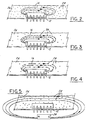
- FIGURE 2 illustrates a microchip actively producing a magnetic field, initially coated with encapsulant, before the ferrite particles migrate along magnetic field lines in accordance with one embodiment of the present invention;
- FIGURE 3 depicts the relative location of the ferrite particles once migration has taken place with respect to the active magnetic field produced by the microchip in accordance with one embodiment of the present invention;
- FIGURE 4 illustrates the overall effect the ferrite particles have on absorbing the active magnetic field once the ferrite particles have migrated and fixed in place by curing in accordance with one embodiment of the present invention;
- FIGURE 5 illustrates a component external to the electronic unit passively producing a magnetic field and where the microchip is initially coated with encapsulant before the ferrite particles migrate along magnetic field lines in accordance with one embodiment of the present invention;
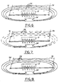
- FIGURE 6 depicts the relative location of the ferrite particles once migration has taken place with respect to the passive magnetic field produced by the external component in accordance with one embodiment of the present invention.
- FIGURE 7 illustrates the overall effect the ferrite particles have on absorbing a passive magnetic field once the ferrite particles have migrated and fixed in place by curing in accordance with one embodiment of the present invention;
- FIGURE 8 depicts ferrite particles absorbing the initial magnetic field in the case where the encapsulant is not cured and the magnetic field is dynamic in nature in accordance with one embodiment of the present invention;
- FIGURE 9 illustrates ferrite particle migration in uncured encapsulant as the characteristics of the dynamic magnetic field change in accordance with one embodiment of the present invention; and
- FIGURE 10 shows the new location of the ferrite particles in uncured encapsulant in response to the changed characteristics of the magnetic field in accordance with one embodiment of the present invention.
-
- In the following figures, the same reference numbers identify identical components in the various views. The present invention illustrates a method for absorbing active, external and dynamic magnetic fields using a ferrite encapsulate coating particularly suited for covering electronic units. However, the present invention also applies to various other uses that may require a method for absorbing active, external and dynamic magnetic fields using a ferrite encapsulate coating.
- Referring to FIGURE 1, a flow diagram illustrating the initial steps of the process 10 to protect an electrical component, such as a
microchip 12, on anelectronic unit 14 frommagnetic field interference 16 in accordance with one embodiment of the present invention is shown. One skilled in the art would realize that the process is merely one representation of many possible processes to use a ferrite encapsulate coating to protect components on anelectronic unit 14. Further, this process can be used to protect other components by coating the radiating component with encapsulant. Additionally, one skilled in the art would realize that microchips 12 are merely one type of electrical component that may need to be protected frommagnetic field interference 16. - The
electronic unit 14 is initially placed inside afixture 18. A number of containment apparatuses, such asmolds 20, can be placed aroundmicrochips 12 that need to be covered with encapsulant (not shown). Themolds 20 serve to provide structure for the encapsulant while still in its liquid state, much like an ice cube tray provides structure for water. One skilled in the art would realize thatmolds 20 are merely one type of containment apparatus that can be used to provide structure for the encapsulant. Once the encapsulant hardens and no longer needs the structural support themolds 20 provide, themolds 20 are removed. In the event the entireelectronic unit 14 must be covered with encapsulant,molds 20 are not used. - In a similar manner, exclusion apparatuses, such as
masks 22, can also be added to theelectronic unit 14.Masks 22 serve to prevent encapsulate from being poured onto components where it is not needed. One skilled in the art would realize that masks 22 are merely one type of exclusion apparatus that can be used to prevent encapsulant from being poured on amicrochip 12. As in the case withmolds 20, if the entireelectronic unit 14 must be covered with encapsulant, masks 22 are not used. - Before encapsulant is poured, a source of
magnetic field interference 16 is needed. Themagnetic field interference 16 can be created actively by themicrochip 12 itself. In this case, apower supply 25 generates the current and voltage necessary to activate themicrochip 12. One skilled in the art will realize that apower supply 25 is merely one many possible ways to activate amicrochip 12. - The
magnetic field interference 16 can also be created passively by an external source. For example, if a first electronic unit were placed in close proximity to a second unit that produced magnetic field interference, the second unit would be a source of magnetic field interference to the first. In the process depicted in FIGURE 1, placing at least onemagnet 24 into thefixture 18 creates passivemagnetic field interference 16. One skilled in the art would realize thatmagnets 24 are merely one way to simulate externalmagnetic field interference 16. The magnet's 24 position in the fixture should mimic the expected location of externalmagnetic field interference 16 themicrochip 12 will experience once theelectronic unit 14 is installed into a product. Similarly, the magnet's 24 strength should mimic the strength of the external magnetic field interference that themicrochip 12 will experience. - Referring to FIGURE 2, a
microchip 12, initially coated withencapsulant 26, actively producingmagnetic field interference 16 according to one embodiment of the present invention is illustrated. Because theferrite particles 28 in theencapsulant 26 have not been allowed time to migrate, their distribution remains random throughout theencapsulant 26. - Referring to FIGURE 3, the relative location of the
ferrite particles 28 after time has been allotted for migration according to one embodiment of the present invention is depicted. The random distribution offerrite particles 28 in FIGURE 2 has given way to a new distribution ordered along the field lines of the activemagnetic field interference 16. Once enough time passes for theferrite particles 28 to migrate to their new location along the field lines, theencapsulant 28 is cured. One skilled in the art will realize that the method used to cure theencapsulant 28 depends upon a number of factors, including, but not limited to, the chemical composition of the ferrite, the microchip's 12 ability to tolerate heat, the speed at which theencapsulant 26 must be cured and whether the entire electronic unit (best seen in FIGURE 1) is coated withencapsulant 26. - Referring to FIGURE 4, the overall effect the
ferrite particles 28 have on absorbing the activemagnetic field interference 16 according to one embodiment of the present invention is illustrated. Once theencapsulant 26 is cured, theferrite particles 28 are fixed in their location along the field lines created by the activemagnetic field interference 16. In this fixed location, theferrite particles 28 will absorb the energy generated by the activemagnetic field interference 16, thus weakening overall field strength. Because of the reduction in field strength, the activemagnetic field interference 16 will have a reduced effect on surrounding components that are sensitive to radiated emissions. - Referring to FIGURE 5, a
microchip 12, initially coated withencapsulant 26 and exposed to passivemagnetic field interference 16 according to one embodiment of the present invention, is illustrated. Here, anexternal magnet 24 passively createsmagnetic field interference 16. As in FIGURE 2, theferrite particles 28 are randomly distributed throughout theencapsulant 26 when the encapsulant is initially applied to themicrochip 12. - Referring to FIGURE 6, the
ferrite particle 28 distribution after migration, while exposed to passivemagnetic field interference 16, according to one embodiment of the present invention is depicted. Here, as in FIGURE 3, theferrite particles 28, originally distributed randomly throughout theencapsulant 26, are now concentrated along the field lines generated by theexternal magnet 24. Once enough time passes to allow most of theferrite particles 28 to migrate to their new location along the field lines of themagnetic field interference 16, theencapsulant 28 is cured. Again, one skilled in the art will realize that the method used to cure theencapsulant 28 depends upon a number of factors, including, but not limited to, the chemical composition of the ferrite, the microchip's 12 ability to tolerate heat, the speed at which theencapsulant 26 must be cured and whether the entire electronic unit (best seen in FIGURE 1)) is coated withencapsulant 26. - Referring to FIGURE 7, the overall effect the
ferrite particles 28 have on absorbing the passivemagnetic field interference 16 according to one embodiment of the present invention is illustrated. Once theencapsulant 26 is cured, theferrite particles 28 are fixed in their location along the field lines created by theexternal magnet 24. In this fixed location, theferrite particles 28 will absorb the energy generated by themagnetic field interference 16, thus weakening overall field strength. Because of the reduction in field strength, the microchip's 12 performance improves. - Referring to FIGURE 8,
ferrite particles 28 absorbing initial dynamicmagnetic field interference 16 when theencapsulant 26 is uncured according to one embodiment of the present invention are depicted. Here, as in FIGURE 6, theferrite particles 28 are concentrated along the field lines generated by theexternal magnet 24. Yet unlike the previous example, themagnetic field interference 30 in this example is dynamic; thus, in order to allow the ferrite particles to freely migrate as the direction or strength of themagnetic field interference 30 changes, theencapsulant 26 is not cured. - Referring to FIGURE 9,
ferrite particle 28 migration when themagnetic field interference 16 characteristics change according to one embodiment of the present invention is illustrated. Because theencapsulant 26 is uncured, the ferrite particles are free to migrate to any location where magnetic interference exists. Here, the direction of themagnetic field interference 30 is changing. Because the natural tendency offerrite particles 28 is to align with the strongest magnetic field present, theferrite particles 28 will migrate from their locations along the "old," fadingmagnetic field interference 30 to new locations along the field lines of the "new"magnetic field interference 32. - Referring to FIGURE 10, the new location of the
ferrite particles 28 in response to the changed characteristics of the dynamicmagnetic field interference 32 is shown. Theferrite particles 28 are now in alignment with the "new"magnetic field interference 32. If the strength or direction of the "new"magnetic field interference 32 changes again in the future, theferrite particles 28, because the encapsulant remains uncured, are free to migrate to yet another new location of magnetic field interference (not shown). - From the foregoing, a new and improved method to absorb magnetic field interference is brought to the art. The preferred embodiment's preceding description merely illustrates one of the many specific applications of the principles utilized in the present invention. Clearly, numerous and other arrangements can be evident to those skilled in the art without departing from the scope of the invention as defined by the following claims:
Claims (10)
- A device to absorb magnetic fields that interfere with electrical components comprising:an electronic unit containing at least one first electrical component requiring a reduction of a magnetic field; andan encapsulant, partially comprised of ferrite particles, wherein said ferrite particles, when exposed to said magnetic field interference, migrate along magnetic field lines and absorb said magnetic field.
- The device as recited in claim 1 wherein said encapsulant comprises a base material comprising a non-conductive liquid polymer with low hygroscopic tendencies and ferrite particles where size and chemical composition of said ferrite particles are adjusted in accordance with magnetic field frequency.
- The device as recited in claim 2 wherein said encapsulant further comprises reactants that enable curing of said encapsulant when said encapsulant is catalytic.
- The device as recited in claim 1 wherein said at least one first electrical component, on said electronic unit, produces said magnetic field.
- The device as recited in claim 1 wherein at least one second component external to said electronic unit produces said magnetic field.
- The device as recited in claim 1 wherein at least one first electrical component produces a dynamic magnetic field.
- The device as recited in claim 1 wherein at least one second component external to said electronic unit produces a dynamic magnetic field.
- A system for absorbing magnetic field interference on an electronic unit comprising:an electronic unit containing at least one first electrical component requiring a reduction of a magnetic field;an encapsulant, partially comprised of ferrite particles, wherein ferrite particle size and chemical composition are adjusted in accordance with magnetic field frequency and wherein said ferrite particles, when exposed to said magnetic field interference, migrate along the magnetic field lines and absorb said magnetic field and wherein said encapsulant is partially comprised of a base material comprising a non-conductive liquid polymer with low hygroscopic tendencies; anda magnetic field wherein said magnetic field adversely affects component performance.
- The system as recited in claim 8 further comprising at least one containment apparatus used to keep said encapsulant on said at least one first electrical component.
- A method for absorbing magnetic field interference comprising the steps of:placing electronic unit into a fixture;exposing said electronic unit to a magnetic field;filling said at least one mold with said encapsulant; andallotting time for said ferrite particles to migrate along magnetic field lines created by said magnetic field.
Applications Claiming Priority (2)
| Application Number | Priority Date | Filing Date | Title |
|---|---|---|---|
| US686189 | 2000-10-11 | ||
| US09/686,189 US6534707B1 (en) | 2000-10-11 | 2000-10-11 | Method for absorbing active, external and dynamic magnetic fields using a ferrite encapsulated coating |
Publications (3)
| Publication Number | Publication Date |
|---|---|
| EP1198165A2 true EP1198165A2 (en) | 2002-04-17 |
| EP1198165A3 EP1198165A3 (en) | 2002-10-16 |
| EP1198165B1 EP1198165B1 (en) | 2004-06-23 |
Family
ID=24755288
Family Applications (1)
| Application Number | Title | Priority Date | Filing Date |
|---|---|---|---|
| EP01124468A Expired - Lifetime EP1198165B1 (en) | 2000-10-11 | 2001-10-11 | Shielding method using a ferrite encapsulate coating |
Country Status (3)
| Country | Link |
|---|---|
| US (1) | US6534707B1 (en) |
| EP (1) | EP1198165B1 (en) |
| DE (1) | DE60103963T2 (en) |
Cited By (4)
| Publication number | Priority date | Publication date | Assignee | Title |
|---|---|---|---|---|
| DE202009017289U1 (en) | 2009-12-22 | 2010-03-25 | Volkswagen Ag | Control panel for operating a mobile phone in a motor vehicle |
| EP2180672A2 (en) | 2008-10-23 | 2010-04-28 | Volkswagen AG | Mobile device system for a motor vehicle |
| DE102009050529A1 (en) | 2009-10-23 | 2011-04-28 | Volkswagen Ag | Mobile device i.e. personal digital assistant, system for land vehicle, has adapter including position determination unit, where position determination unit calculates proposed route from location of adapter to destination |
| CN105556659A (en) * | 2013-10-15 | 2016-05-04 | 英特尔公司 | Magnetic shielded integrated circuit package |
Families Citing this family (10)
| Publication number | Priority date | Publication date | Assignee | Title |
|---|---|---|---|---|
| GB0104910D0 (en) * | 2001-02-28 | 2001-04-18 | Ibm | Devices to reduce electro-magnetic field radiation |
| JP3916889B2 (en) * | 2001-06-08 | 2007-05-23 | ソニー株式会社 | Semiconductor sealing resin composition and semiconductor device using the same |
| US7730823B1 (en) * | 2005-01-15 | 2010-06-08 | Cedar Ridge Research Llc | Magnetic damping field armor system and method |
| KR101316479B1 (en) * | 2005-06-24 | 2013-10-08 | 레오나르트 쿠르츠 스티프퉁 운트 코. 카게 | Method of preparing electrode |
| US20070017568A1 (en) * | 2005-07-12 | 2007-01-25 | Howard Berke | Methods of transferring photovoltaic cells |
| WO2007011742A2 (en) * | 2005-07-14 | 2007-01-25 | Konarka Technologies, Inc. | Cigs photovoltaic cells |
| DE102005046908A1 (en) * | 2005-09-30 | 2007-04-05 | Merck Patent Gmbh | Electrochemical deposition of gray selenium on substrate e.g. non-metal, metalloid, metal, alloy or conductive and metallized ceramic or plastics for use as photosemiconductor in photovoltaics or electronics is carried out from ionic liquid |
| US9121885B2 (en) * | 2010-08-16 | 2015-09-01 | Infineon Technologies Ag | Sensor package and method of manufacturing thereof |
| EP2461657A1 (en) * | 2010-12-02 | 2012-06-06 | Siemens Aktiengesellschaft | Electric assembly and method for producing an assembly |
| US10856455B1 (en) * | 2019-09-05 | 2020-12-01 | The Boeing Company | Electromagnetic interference shielding panels and associated methods |
Citations (4)
| Publication number | Priority date | Publication date | Assignee | Title |
|---|---|---|---|---|
| EP0588574A1 (en) * | 1992-09-11 | 1994-03-23 | Uniden Corporation | Electro-magnetic wave shielding structure |
| US5374779A (en) * | 1992-07-22 | 1994-12-20 | Uniden Corporation | Electro-magnetic wave shielding structure |
| US5785913A (en) * | 1996-05-30 | 1998-07-28 | Westinghouse Electric Corporation | Method of magnetically forming a particle filled polymer having enhanced material characteristics |
| GB2345799A (en) * | 1997-08-19 | 2000-07-19 | Taiyo Yuden Kk | Filler material for a wire wound electronic component |
Family Cites Families (11)
| Publication number | Priority date | Publication date | Assignee | Title |
|---|---|---|---|---|
| US4188605A (en) | 1978-07-21 | 1980-02-12 | Stout Glenn M | Encapsulated Hall effect device |
| JPS6018145B2 (en) | 1980-09-22 | 1985-05-09 | 株式会社日立製作所 | Resin-encapsulated semiconductor device |
| JPS59158016A (en) | 1983-02-28 | 1984-09-07 | ティーディーケイ株式会社 | Electromagnetically shielding material |
| US4698197A (en) * | 1985-02-12 | 1987-10-06 | The United States Of America As Represented By The United States Department Of Energy | Magnetic shielding |
| US5547599A (en) | 1989-03-17 | 1996-08-20 | Raytheon Company | Ferrite/epoxy film |
| US5371404A (en) | 1993-02-04 | 1994-12-06 | Motorola, Inc. | Thermally conductive integrated circuit package with radio frequency shielding |
| FI117224B (en) * | 1994-01-20 | 2006-07-31 | Nec Tokin Corp | Electromagnetic interference suppression piece, applied by electronic device and hybrid integrated circuit element |
| US5677511A (en) | 1995-03-20 | 1997-10-14 | National Semiconductor Corporation | Overmolded PC board with ESD protection and EMI suppression |
| US5709960A (en) | 1996-06-21 | 1998-01-20 | Motorola, Inc. | Mold compound |
| EP0977251B1 (en) * | 1997-02-10 | 2011-11-16 | Panasonic Corporation | Resin sealed semiconductor device and method for manufacturing the same |
| US6190509B1 (en) * | 1997-03-04 | 2001-02-20 | Tessera, Inc. | Methods of making anisotropic conductive elements for use in microelectronic packaging |
-
2000
- 2000-10-11 US US09/686,189 patent/US6534707B1/en not_active Expired - Fee Related
-
2001
- 2001-10-11 DE DE60103963T patent/DE60103963T2/en not_active Expired - Fee Related
- 2001-10-11 EP EP01124468A patent/EP1198165B1/en not_active Expired - Lifetime
Patent Citations (4)
| Publication number | Priority date | Publication date | Assignee | Title |
|---|---|---|---|---|
| US5374779A (en) * | 1992-07-22 | 1994-12-20 | Uniden Corporation | Electro-magnetic wave shielding structure |
| EP0588574A1 (en) * | 1992-09-11 | 1994-03-23 | Uniden Corporation | Electro-magnetic wave shielding structure |
| US5785913A (en) * | 1996-05-30 | 1998-07-28 | Westinghouse Electric Corporation | Method of magnetically forming a particle filled polymer having enhanced material characteristics |
| GB2345799A (en) * | 1997-08-19 | 2000-07-19 | Taiyo Yuden Kk | Filler material for a wire wound electronic component |
Cited By (7)
| Publication number | Priority date | Publication date | Assignee | Title |
|---|---|---|---|---|
| EP2180672A2 (en) | 2008-10-23 | 2010-04-28 | Volkswagen AG | Mobile device system for a motor vehicle |
| DE102009050579A1 (en) | 2008-10-23 | 2010-04-29 | Bury Gmbh & Co. Kg | Mobile device system for a motor vehicle |
| DE102009050529A1 (en) | 2009-10-23 | 2011-04-28 | Volkswagen Ag | Mobile device i.e. personal digital assistant, system for land vehicle, has adapter including position determination unit, where position determination unit calculates proposed route from location of adapter to destination |
| DE102009050529B4 (en) | 2009-10-23 | 2020-06-04 | Volkswagen Ag | Mobile device system for a motor vehicle |
| DE202009017289U1 (en) | 2009-12-22 | 2010-03-25 | Volkswagen Ag | Control panel for operating a mobile phone in a motor vehicle |
| DE202010001964U1 (en) | 2009-12-22 | 2010-04-22 | Volkswagen Ag | Control panel for operating a mobile phone in a motor vehicle |
| CN105556659A (en) * | 2013-10-15 | 2016-05-04 | 英特尔公司 | Magnetic shielded integrated circuit package |
Also Published As
| Publication number | Publication date |
|---|---|
| DE60103963D1 (en) | 2004-07-29 |
| DE60103963T2 (en) | 2005-07-14 |
| US6534707B1 (en) | 2003-03-18 |
| EP1198165A3 (en) | 2002-10-16 |
| EP1198165B1 (en) | 2004-06-23 |
Similar Documents
| Publication | Publication Date | Title |
|---|---|---|
| US6534707B1 (en) | Method for absorbing active, external and dynamic magnetic fields using a ferrite encapsulated coating | |
| ES2656009T3 (en) | Powder coating method and apparatus for absorbing electromagnetic interference (EMI) | |
| EP2277179B1 (en) | Magnetically controlled polymer nanocomposite material and methods for applying and curing same, and nanomagnetic composite for rf applications | |
| US9991211B2 (en) | Semiconductor package having an EMI shielding layer | |
| US6350951B1 (en) | Electric shielding of on-board devices | |
| JPH077099A (en) | Package for integrated circuit and attenuation of electromagnetic radiation | |
| US5547599A (en) | Ferrite/epoxy film | |
| EP4350442A2 (en) | Patterned materials and films and systems and methods for making the same | |
| CA2278838A1 (en) | Methods and compositions for ionizing radiation shielding | |
| JP2002020637A (en) | Sealing or embedding compound having electromagnetic shielding properties for manufacturing electronic part | |
| JP2004200534A (en) | Electromagnetic wave absorbing thermal conductive sheet | |
| US20030117786A1 (en) | Electromagnetic interference waveguide shield with absorber layer | |
| US20190232582A1 (en) | Composite Materials, and Systems and Methods for Making Composite Materials | |
| JPH073195U (en) | Exterior structure of hybrid integrated circuit parts | |
| JP2005286191A (en) | Laminated electromagnetic wave absorber | |
| JPH039823A (en) | Method and apparatus for molding electrically conductive resin | |
| JPS60101011A (en) | Manufacture of resin molded item | |
| US6376922B1 (en) | Radio frequency-transmissive compositions, methods of forming radio frequency-transmissive compositions, microelectronic devices wireless radio frequency communication devices, and methods of forming microelectronic devices, wireless radio frequency communication devices | |
| JPH03129897A (en) | Composite electromagnetic shielding material | |
| JPS60186040A (en) | Electronic part | |
| JPH05110283A (en) | Plastic box body and molding method thereof | |
| JPS6074497A (en) | Electromagnetic wave shielding material | |
| JP2001284877A (en) | Material for electromagnetic wave shields | |
| US20030002240A1 (en) | Electrical device having components arranged in a casing and outwardly electromagnetically shielded | |
| KR20200000579U (en) | Radiative cooling structure of wireless charging device |
Legal Events
| Date | Code | Title | Description |
|---|---|---|---|
| PUAI | Public reference made under article 153(3) epc to a published international application that has entered the european phase |
Free format text: ORIGINAL CODE: 0009012 |
|
| AK | Designated contracting states |
Kind code of ref document: A2 Designated state(s): AT BE CH CY DE DK ES FI FR GB GR IE IT LI LU MC NL PT SE TR |
|
| AX | Request for extension of the european patent |
Free format text: AL;LT;LV;MK;RO;SI |
|
| 17P | Request for examination filed |
Effective date: 20020613 |
|
| PUAL | Search report despatched |
Free format text: ORIGINAL CODE: 0009013 |
|
| AK | Designated contracting states |
Kind code of ref document: A3 Designated state(s): AT BE CH CY DE DK ES FI FR GB GR IE IT LI LU MC NL PT SE TR |
|
| AX | Request for extension of the european patent |
Free format text: AL;LT;LV;MK;RO;SI |
|
| RIC1 | Information provided on ipc code assigned before grant |
Free format text: 7H 05K 9/00 A, 7H 01Q 17/00 B |
|
| 17Q | First examination report despatched |
Effective date: 20030303 |
|
| AKX | Designation fees paid |
Designated state(s): DE FR GB |
|
| GRAP | Despatch of communication of intention to grant a patent |
Free format text: ORIGINAL CODE: EPIDOSNIGR1 |
|
| GRAS | Grant fee paid |
Free format text: ORIGINAL CODE: EPIDOSNIGR3 |
|
| GRAA | (expected) grant |
Free format text: ORIGINAL CODE: 0009210 |
|
| AK | Designated contracting states |
Kind code of ref document: B1 Designated state(s): DE FR GB |
|
| REG | Reference to a national code |
Ref country code: GB Ref legal event code: FG4D |
|
| REG | Reference to a national code |
Ref country code: IE Ref legal event code: FG4D |
|
| REF | Corresponds to: |
Ref document number: 60103963 Country of ref document: DE Date of ref document: 20040729 Kind code of ref document: P |
|
| ET | Fr: translation filed | ||
| PLBE | No opposition filed within time limit |
Free format text: ORIGINAL CODE: 0009261 |
|
| STAA | Information on the status of an ep patent application or granted ep patent |
Free format text: STATUS: NO OPPOSITION FILED WITHIN TIME LIMIT |
|
| 26N | No opposition filed |
Effective date: 20050324 |
|
| PGFP | Annual fee paid to national office [announced via postgrant information from national office to epo] |
Ref country code: FR Payment date: 20051014 Year of fee payment: 5 |
|
| REG | Reference to a national code |
Ref country code: FR Ref legal event code: ST Effective date: 20070629 |
|
| PGFP | Annual fee paid to national office [announced via postgrant information from national office to epo] |
Ref country code: DE Payment date: 20071025 Year of fee payment: 7 |
|
| PG25 | Lapsed in a contracting state [announced via postgrant information from national office to epo] |
Ref country code: FR Free format text: LAPSE BECAUSE OF NON-PAYMENT OF DUE FEES Effective date: 20061031 |
|
| PGFP | Annual fee paid to national office [announced via postgrant information from national office to epo] |
Ref country code: GB Payment date: 20071023 Year of fee payment: 7 |
|
| GBPC | Gb: european patent ceased through non-payment of renewal fee |
Effective date: 20081011 |
|
| PG25 | Lapsed in a contracting state [announced via postgrant information from national office to epo] |
Ref country code: DE Free format text: LAPSE BECAUSE OF NON-PAYMENT OF DUE FEES Effective date: 20090501 |
|
| PG25 | Lapsed in a contracting state [announced via postgrant information from national office to epo] |
Ref country code: GB Free format text: LAPSE BECAUSE OF NON-PAYMENT OF DUE FEES Effective date: 20081011 |