EP1198099A2 - GMSK modulator, using direct digital synthesis - Google Patents
GMSK modulator, using direct digital synthesis Download PDFInfo
- Publication number
- EP1198099A2 EP1198099A2 EP01308640A EP01308640A EP1198099A2 EP 1198099 A2 EP1198099 A2 EP 1198099A2 EP 01308640 A EP01308640 A EP 01308640A EP 01308640 A EP01308640 A EP 01308640A EP 1198099 A2 EP1198099 A2 EP 1198099A2
- Authority
- EP
- European Patent Office
- Prior art keywords
- unit
- processor
- data
- input
- phase
- Prior art date
- Legal status (The legal status is an assumption and is not a legal conclusion. Google has not performed a legal analysis and makes no representation as to the accuracy of the status listed.)
- Withdrawn
Links
Images




Classifications
-
- H—ELECTRICITY
- H04—ELECTRIC COMMUNICATION TECHNIQUE
- H04L—TRANSMISSION OF DIGITAL INFORMATION, e.g. TELEGRAPHIC COMMUNICATION
- H04L25/00—Baseband systems
- H04L25/02—Details ; arrangements for supplying electrical power along data transmission lines
- H04L25/03—Shaping networks in transmitter or receiver, e.g. adaptive shaping networks
- H04L25/03828—Arrangements for spectral shaping; Arrangements for providing signals with specified spectral properties
- H04L25/03834—Arrangements for spectral shaping; Arrangements for providing signals with specified spectral properties using pulse shaping
-
- H—ELECTRICITY
- H04—ELECTRIC COMMUNICATION TECHNIQUE
- H04L—TRANSMISSION OF DIGITAL INFORMATION, e.g. TELEGRAPHIC COMMUNICATION
- H04L27/00—Modulated-carrier systems
- H04L27/18—Phase-modulated carrier systems, i.e. using phase-shift keying
- H04L27/20—Modulator circuits; Transmitter circuits
- H04L27/2003—Modulator circuits; Transmitter circuits for continuous phase modulation
- H04L27/2007—Modulator circuits; Transmitter circuits for continuous phase modulation in which the phase change within each symbol period is constrained
- H04L27/2017—Modulator circuits; Transmitter circuits for continuous phase modulation in which the phase change within each symbol period is constrained in which the phase changes are non-linear, e.g. generalized and Gaussian minimum shift keying, tamed frequency modulation
Definitions
- the present invention relates to modulation and demodulation for signal transmission, for example GMSK (Gaussian Minimum Shift Keying) modulation.
- GMSK Global System for Mobile Communications
- GMSK Global System for Mobile Communications
- GMSK provides improved spectral efficiency (mainlobe-to-sidelobe energy) compared with other modulation techniques such as MSK, but with more complexity in the receiver. This disadvantage can be reduced if the GMSK detection process is combined with channel equalisation to remove the effect of ISI (controlled and channel induced) in one go. This is typically achieved in GSM through the use of the well-known Viterbi Algorithm.
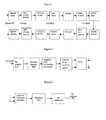
- Figure 1 shows a block diagram for a GSM system. The blocks of main interest herein are those marked “GMSK Mod.” and "GMSK demod".
- the GMSK module can be implemented either in hardware in the RF section or as a baseband function in a Digital Signal Processor (DSP), or in firmware.
- DSP Digital Signal Processor
- GMSK baseband processing is conventionally achieved using a DSP but the processing can be achieved efficiently using table look-ups.
- Such a system is disclosed in US patent 5,022,054.
- MIP's processing power
- ROM capacity are very high. This has a large and undesirable effect on power consumption and thus battery life.
- Such a high level of functionality has been achieved in mobile telephones and the like that now, possibly, the most important sales criteria is battery size/life.
- a signal processor for modulating and/or demodulating input data containing phase information
- the processor comprising: a data input unit for receiving the input data, a memory unit for storing a look up table addressable by the input data, a multiplexer unit for multiplexing outputs from the memory unit, an accumulated phase unit for extracting phase information from the input data, and a digital-to-analog converter for receiving an input from the multiplexer unit and providing the output of the signal processor, characterised in that the accumulated phase unit is connected between the data input unit and the multiplexer unit so as to bypass the memory unit and in that a bypass path is connected between the data input unit and the digital-to-analog converter so as to enable part of the input data to bypass the memory unit.
- the signal processor according to the first aspect of the invention further comprising a coordinate rotation processor connected for processing the output of memory unit before it is passed to the multiplexer unit.
- a signal processor for modulating and/or demodulating input data containing phase information
- the processor comprising: a data input unit for receiving the input data, a coordinate rotation processor connected to receive data from the data input unit, and a digital-to-analog converter for receiving an input from the coordinate rotation processor and providing the output of the signal processor, characterised in that the coordinate rotation processor is arranged so as to use the received data to calculate a correlative phase state as well as perform iterative phase rotations while also deriving an accumulated phase angle.
- the coordinate rotation processor is a bit-serial recursive processor.
- a method of signal processing comprising modulating and/or demodulating input data containing phase information using a processor having: a data input unit, a memory unit, a multiplexer unit, an accumulated phase unit, and a digital-to-analog converter, the method comprising the steps of: applying the input data to the data input unit, storing in the memory unit a look up table addressable by the input data, multiplexing outputs from the memory in the multiplexer unit, extracting phase information from the input data using the accumulated phase unit, and converting the output of the multiplexer unit to provide an analog output using the digital-to-analog converter, characterised by passing the extracted phase information to the multiplexer unit so as to bypass the memory unit and applying part of the input data to the digital-to-analog converter so that said part of the input data bypasses the memory unit.
- the method of signal processing according to the third aspect of the invention further comprising the step of performing an iterative process to calculate cos and sin values from phase angle information output from the memory unit and applying the calculated cos and sin values to the multiplexer unit for the multiplexing step.
- the step of performing an iterative process consists of add/subtract operations and a right bit shift operation.
- the iterative process involves the application of successive phase rotations with a convergence towards zero.
- a method of signal processing comprising modulating and/or demodulating input data containing phase information using a processor having: a data input unit, for receiving the input data, a coordinate rotation processor connected to receive data from the data input unit, and a digital-to-analog converter for receiving an input from the coordinate rotation processor and providing the output of the signal processor, characterised by: performing calculation of a correlative phase state; performing iterative phase rotations; and deriving an accumulated phase angle all within the coordinate rotation processor.
- the input to the GMSK modulator is a 271 kbit/s data stream organised as a GSM 'normal' burst with 8 TDMA coded speech channels and a 26-bit preamble inserted in the middle of the burst.
- This baseband data stream must be converted to the 900 MHz frequency band by some combination of spectral shaping and frequency translation. This is conventionally achieved using the baseband/passband split indicated in figures 2 and 3.
- the baseband processing is performed in a DSP and the RF processing is special purpose high-frequency hardware. It is notoriously difficult to achieve the required balance between the quadrature oscillators and the desired frequency stability on the transmitted carrier, especially at the high RF frequencies used in GSM (900 MHz).
- the incoming data ('Normal' burst) at 271 kbit/s is first up-sampled by inserting zeros between successive data symbols. For example, if the up-sampling ratio is 8 (which gives a sampling rate for the GMSK transmitter of 2.168 MHz) then each data symbol (+1 or -1) is followed by 7 zeros.
- the Gaussian shaping filter which is typically implemented as a Finite Impulse Response (FIR) digital filter.
- FIR Finite Impulse Response
- Controlled intersymbol interference is added by extending the influence of the Gaussian shaping filter over L data symbol intervals (i.e. the FIR time span is L.T, where T is the symbol duration).
- L is in the range 2 to 4.
- the Gaussian shaping filter requires 32 coefficients (4 x 8) and approximately 64 MIP's (32 x 2.168) for this part of the GMSK transmitter alone. This is much more than a normal DSP can handle.
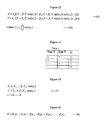
- phase angle delivered to the phase modulator by the Gaussian shaping filter is given by equation 2 shown in figure 5, in which ⁇ ( t , ⁇ ) is the correlative state vector that depends on the L most recent symbols currently in the shaping filter.
- the second term ⁇ n is the accumulated phase of all the previous symbols that have passed through the filter and is referred to as the phase state. It is here noted that if the modulation index (h F ) is 0.5, then the phase state can only have the values of 0, ⁇ /2, - ⁇ /2, or ⁇ (i.e. 4 values). If the modulation index is 0.3 then the phase state can have six values (i.e. 0, ⁇ /3, - ⁇ /3, 2 ⁇ /3, -2 ⁇ /3 and ⁇ ).
- the final stage of baseband processing for the GMSK transmitter is the conversion of phase to the I and Q values for passing to the RF transmitter. This can be completed algorithmically or it can be implemented as a look-up table. Simulations have shown that 256 values, each producing an 8-bit value for COS( ⁇ ) and SIN( ⁇ ) are sufficient to meet the GSM transmit power/frequency mask.
- the input data are an over-sampled set of restricted data symbols (+1, 0 or - 1) and that this also applies to the accumulated phase state ⁇ n , it is possible to replace the processing in figure 2 with the Simplified GMSK Baseband Transmitter shown in figure 6.
- the data input is applied to a shift register which outputs 3 bits ⁇ (t, ⁇ ) to the look-up table.
- Phase information is extracted from the shift register output and, using a feedback loop, the accumulated phase ⁇ n is derived.
- the accumulated phase information is applied to the look up table as 2 bits.
- the sample timing is also applied to the look up table, as the final 3 bits making up the full 8 bit input to the table.
- the 8-bit output values from the look up table (ROM) are then multiplexed (indicated by MUX in figure 6) before being converted to analogue I, Q values (in the DAC unit) for the RF section.
- the present invention improves upon the design shown in figure 6 so as dramatically to reduce the amount of ROM required, and hence the chip area and power dissipation.
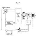
- the circuit of figure 7 includes a shift register receiving the data input, a look up table implemented as a ROM, a three bit sampling time input to the ROM, 8 bit I/Q outputs to a multiplexer (MUX) and a digital to analog converter (DAC).
- MUX multiplexer
- DAC digital to analog converter
- the accumulated phase information is not input in to the look up table but is processed separately therefrom. That is, by recognising that the accumulated phase can only have values which are multiples of ⁇ /2, the phase angle delivered to the modulator (MUX) consists of simple 90 degree rotations of the phase output from the Gaussian filter.
- the phase information is simply used to rotate the outputs I/Q. This is achieved by feeding the accumulated phase information to a pair of ExOr gates, applying the output therefrom to a select logic, the output of which is feed to the modulator.
- the select logic implements a simple table, Table 1 (see figure 7), which provides the required 90 degree rotations.
- symmetries in the input data are exploited by only storing the 'positive' values of the 3 bit input sequence in the ROM.
- the requirements for the ROM can be reduced by a still further factor of two.
- This embodiment uses a processor to convert from ⁇ to COS( ⁇ n ) and SIN( ⁇ n ). Consequently the ROM only needs to store the values of ⁇ , thus reducing the ROM storage by a further factor of 2.
- the processor can be useful elsewhere in the GSM system (e.g. in the demodulator/equaliser), and the burden of this additional circuitry can thus be reduced.
- the circuit arrangement of this second embodiment is shown in figure 8, wherein the processor is annotated "CORDIC", which is an abbreviation used herein to mean "Coordinate Rotation DIgital Computer".
- the ROM requirements are reduced to 32 locations each storing a cos( ⁇ ) and a sin( ⁇ ) value.
- the bulk of the complexity in a GMSK transmitter using such an embodiment is in generating these Cartesian components from the Gaussian filtered phase angle.
- a typical DSP has two arithmetic processing units, one of which is optimised for bit manipulation operations.
- this BLU Bit Logic Unit
- MAC Multiple Add Cycles
- equation 4 also involves an amplitude scaling (by cos( ⁇ )) but this is completely defined and can be allowed for by scaling the final output when the iterative phase rotation algorithm (to be described) has been completed. Indeed for applications like GMSK, which is a constant amplitude modulation technique, this amplitude scaling can often be ignored.
- the first step is unique in that a perfect rotation step is performed.
- the value ⁇ i of the rotated vector is determined by examining the sign of the value of Y ' i-1 indicated in figure 15.
- the subsequent rotation is always such that this value converges towards 0.
- Y ' n should be very close to zero, and the desired phase angle is obtained according to equation 8, shown in figure 16. For an angle accuracy of less than 1° then at least 8 rotation steps are required.
- the iterative processing described above is simple to carry out either in hardware or in DSP firmware.
- the algorithm requires a total of 3 registers (for the X, Y and ⁇ values).
- a right-shift (power-of-two) operation is required for successive iterations, and the ability to add or subtract two numbers is needed. This is all available in the Bit Arithmetic Logic unit of a typical DSP processor.
- figure 17 gives an example of the technique implemented in bit-serial recursive hardware which is suitable for implementation in an ASIC.
- the second embodiment of the invention iteratively performs Polar-to-Cartesian conversion, using only power-of-two scaling operations and the simple addition/subtraction of two numbers. Unlike conventional Polar-to-Cartesian conversion, no multipliers, Taylor Series expansions or large look-up tables are required. This form of processing readily lends itself to DSP architecture which will typically have a relatively under-utilised BLU which is highly optimised for this type of processing.
- this invention provides an implementation of a GMSK transmitter using only a small look-up table and a few simple external components.
- the gaussian filter can be implemented in ROM and the Integrator/COS( ⁇ n ), SIN( ⁇ n ) look-up table implemented using the highly efficient digital CORDIC in hardware.
- the address for the ROM can also easily be performed in the DSP.
- a look-up is used to calculate the combined operations of Gaussian filtering and polar-to cartesian conversion of ⁇ to sin( ⁇ ) and cos( ⁇ ).
- the correlative state vector ⁇ ( t , ⁇ ) is in the same form as that involved in the iterative phase rotations in the CORDIC (c.f. equation 8).
- the same part of the CORDIC hardware that performs these iterations can be used to derive the correlative state vector.
- the correlative state vector can be calculated efficiently using the hardware already available for the basic CORDIC.
- the overall clock speed may increase slightly to perform the additional phase additions or subtractions.
- the angle calculations used in the basic CORDIC operation use a small local memory to store the rotation angle values (equation 5, and as shown in figure 17). Therefore, it is possible to extend this table to include the Gaussian filter coefficients and extend the select and angle accumulation process to include these values.
- the actual set of Gaussian coefficients that is used in a given sampling interval is determined by the 'sample time index' box in figure 18.
- the accumulated phase angle can be readily incorporated with a further iteration. Indeed, by allowing the phase angle to accumulate between successive conversions (i.e. by not resetting the phase register to zero each time) the accumulated phase can be generated directly within the CORDIC. This avoids the need to calculate this explicitly in a separate accumulator.
- Equation 2 the resultant phase angle (equation 2) is then rotated by a series of angles, ⁇ (equation 5), in accordance with the normal CORDIC operation, as is described above.
- the iterative processing described above is relatively simple to carry out either in hardware or in DSP firmware.
- the algorithm requires a total of 3 registers (for the X, Y and ⁇ values).
- a right-shift (power-of-two) operation is required for successive iterations, and the ability to add or subtract two numbers is needed. This is relatively easy to implement with modern ASIC (Application Specific Integrated Circuit) hardware techniques.
- figure 17 is an example of the technique implemented in bit-serial recursive hardware, which is suitable for implementation in a relatively small ASIC.
- Other processing structures are possible using bit-parallel processing, pipelining of CORDIC rotations etc.
- the CORDIC technique described above reduces the input ROM requirement for GMSK by exploiting a CORDIC iterative rotation algorithm, which enables polar-to-cartesian conversion using only power-of-two scaling operations and the simple addition/subtraction of numbers. Unlike conventional polar-to-cartesian conversion, no multipliers, Taylor series expansions or large look-up tables are required. Hence it lends itself to relatively simple hardware implementation.
- the present invention provides an implementation of a GMSK transmitter using a CORDIC, extended by a small look-up table.
- a device embodying the present invention can have the advantage that it can be easily controlled by an efficient power management system (driven by the VAD - Voice Activity Detector) to turn off the transmitter and hence conserve handset battery life. This is not so easily achieved in conventional DSP's if the GMSK baseband processing is performed algorithmically.
Landscapes
- Engineering & Computer Science (AREA)
- Physics & Mathematics (AREA)
- Computer Networks & Wireless Communication (AREA)
- Signal Processing (AREA)
- Nonlinear Science (AREA)
- Spectroscopy & Molecular Physics (AREA)
- Power Engineering (AREA)
- Digital Transmission Methods That Use Modulated Carrier Waves (AREA)
Abstract
Description
- Design A:
- All Gaussian filtering was performed in the DSP as a conventional Finite-Impulse-Response (FIR) operation.
- Design B:
- All the GMSK processing was performed in a ROM table look-up (as per Fig. 6). Two ROM tables are required (for the Sin() and Cos() tables). The address calculation can be readily performed on either the DSP or as external random-logic. In either case it is assumed that no additional DSP cycles are required for ROM address calculation.
- Design C:
- The GMSK processing was implemented using the simplified structure of figure 7, in accordance with the first embodiment of the present invention.
- Design D:
- The GMSK processing was implemented as a combination of ROM table look-up and CORDIC processing and implemented as shown in figure 8, in accordance with the second embodiment of the present invention.
- Oversampling ratio = 8,
- Modulation index = .5,
- Gaussian filter time span = 4T
- ROM accuracy = 8 bits/word,
- Angle accuracy (Cordic) < 1 deg.
- Input data rate = 271 kbit/s,
- Output data rate = 2.168 MHz (to the RF stage)
| GMSK Complexity & Power | ||||||
| GMSK Design | ROM Size Bytes | ROM Gates Count | RL Gates Count | Total Gates Count | Total DSP MIPs | Power mW |
| Design A | 512 | 40960 | 0 | 40960 | 13 | 50 |
| Design B | 512 | 40960 | 103 | 41063 | 0 | 22.3 |
| Design C | 64 | 5120 | 195 | 5315 | 0 | 2.9 |
| Design D | 32 | 2560 | 195 | 2755 | 0 | 1.5 |
- 10 gates needed per ROM bit, including address decoding
- Exclusive-Or operation needs 3 BC gates
- Shift-register needs 9 BC gates/bit
- 2-bit adder needs 10 BC gates
- 3-bit counter requires 48 BC gates (approx)
- Design A requires 4 MAC operations + 2 additions (for the integrated phase state)
- ROM Address generation for Design B requires no DSP cycles (i.e. can be performed in parallel)
- Cordic processing for Design C can be performed in parallel in the DSP using the BLU (for example).
- For better than 1 deg. of accuracy for the phase angle the Cordic requires 8 rotational steps.
- I/O between the DSP and ROM has been ignored since no design offers any particular advantage/disadvantage. I/O power dissipation is heavily technology dependant and in any case ROM look-up may be performed on-chip for small ROM look-up tables (as in designs C and D).
- Power dissipation is based on a standard DSPOakCore (running at 60MHz), and the power dissipation per BC Gate is based on the EPSON 50000 Series .35 µm CMOS process. At 3.3V the power per BC gate is assumed to be 0.25 µW/MHz.
- Interprocess and bus drivers have not been included in the power calculations. The DAC and Mux have also been ignored for comparison purposes.
Claims (21)
- A signal processor for modulating and/or demodulating input data containing phase information, the processor comprising: a data input unit for receiving the input data, a memory unit for storing a look up table addressable by the input data, a multiplexer unit for multiplexing outputs from the memory unit, an accumulated phase unit for extracting phase information from the input data, and a digital-to-analog converter for receiving an input from the multiplexer unit and providing the output of the signal processor, characterised in that the accumulated phase unit is connected between the data input unit and the multiplexer unit so as to bypass the memory unit and in that a bypass path is connected between the data input unit and the digital-to-analog converter so as to enable part of the input data to bypass the memory unit.
- A signal processor as claimed in claim 1, further comprising a coordinate rotation processor connected for processing the output of memory unit before it is passed to the multiplexer unit.
- A signal processor for modulating and/or demodulating input data containing phase information, the processor comprising: a data input unit for receiving the input data, a coordinate rotation processor connected to receive data from the data input unit, and a digital-to-analog converter for receiving an input from the coordinate rotation processor and providing the output of the signal processor, characterised in that the coordinate rotation processor is arranged so as to use the received data to calculate a correlative phase state as well as perform iterative phase rotations while also deriving an accumulated phase angle.
- A signal processor as claimed in claim 3, in which the coordinate rotation processor comprises a memory unit having stored therein rotation angle values and Gaussian filter coefficients.
- A signal processor as claimed in claim any of claim 2 to 4, wherein the coordinate rotation processor is a bit-serial recursive processor.
- A transmitter containing a signal processor as claimed in any preceding claim.
- A receiver containing a signal processor as claimed in any of claims 1 to 5.
- A method of signal processing comprising modulating and/or demodulating input data containing phase information using a processor having: a data input unit, a memory unit, a multiplexer unit, an accumulated phase unit, and a digital-to-analog converter, the method comprising the steps of: applying the input data to the data input unit, storing in the memory unit a look up table addressable by the input data, multiplexing outputs from the memory in the multiplexer unit, extracting phase information from the input data using the accumulated phase unit, and converting the output of the multiplexer unit to provide an analog output using the digital-to-analog converter, characterised by passing the extracted phase information to the multiplexer unit so as to bypass the memory unit and applying part of the input data to the digital-to-analog converter so that said part of the input data bypasses the memory unit.
- A method of signal processing as claimed in claim 8, further comprising the step of performing an iterative process to calculate cos and sin values from phase angle information output from the memory unit and applying the calculated cos and sin values to the multiplexer unit for the multiplexing step.
- A method of signal processing as claimed in claim 9, wherein the step of performing an iterative process consists of add/subtract operations and a right bit shift operation.
- A method of signal processing as claimed in claim 9, wherein the iterative process involves the application of successive phase rotations with a convergence towards zero.
- A method of signal processing comprising modulating and/or demodulating input data containing phase information using a processor having: a data input unit, for receiving the input data, a coordinate rotation processor connected to receive data from the data input unit, and a digital-to-analog converter for receiving an input from the coordinate rotation processor and providing the output of the signal processor, characterised by: performing calculation of a correlative phase state; performing iterative phase rotations; and deriving an accumulated phase angle all within the coordinate rotation processor.
- A method as claimed in claim 12, further comprising the step of using a single memory unit within the coordinate rotation processor to store rotation angle values and Gaussian filter coefficients.
- A signal processor substantially as hereinbefore described with reference to and as illustrated in figure 7 of the accompanying drawings.
- A signal processor substantially as hereinbefore described with reference to and as illustrated in figure 8 of the accompanying drawings.
- A signal processor substantially as hereinbefore described with reference to and as illustrated in figures 8 and 17 of the accompanying drawings.
- A signal processor substantially as hereinbefore described with reference to and as illustrated in figures 8 and 18 of the accompanying drawings.
- A method of signal processing substantially as hereinbefore described with reference to and as illustrated in figure 7 of the accompanying drawings.
- A method of signal processing substantially as hereinbefore described with reference to and as illustrated in figure 8 of the accompanying drawings.
- A method of signal processing substantially as hereinbefore described with reference to and as illustrated in figures 8 and 17 of the accompanying drawings.
- A method of signal processing substantially as hereinbefore described with reference to and as illustrated in figures 8 and 18 of the accompanying drawings.
Applications Claiming Priority (2)
| Application Number | Priority Date | Filing Date | Title |
|---|---|---|---|
| GB0024799A GB2368244A (en) | 2000-10-10 | 2000-10-10 | Signal processor with look-up table for modulating data |
| GB0024799 | 2000-10-10 |
Publications (2)
| Publication Number | Publication Date |
|---|---|
| EP1198099A2 true EP1198099A2 (en) | 2002-04-17 |
| EP1198099A3 EP1198099A3 (en) | 2003-12-03 |
Family
ID=9901001
Family Applications (1)
| Application Number | Title | Priority Date | Filing Date |
|---|---|---|---|
| EP01308640A Withdrawn EP1198099A3 (en) | 2000-10-10 | 2001-10-10 | GMSK modulator, using direct digital synthesis |
Country Status (2)
| Country | Link |
|---|---|
| EP (1) | EP1198099A3 (en) |
| GB (2) | GB2368244A (en) |
Cited By (4)
| Publication number | Priority date | Publication date | Assignee | Title |
|---|---|---|---|---|
| WO2005109806A1 (en) * | 2004-05-12 | 2005-11-17 | Telefonaktiebolaget L M Ericsson (Publ) | A method and apparatus to reduce undesired amplitude modulation |
| WO2007016274A3 (en) * | 2005-07-29 | 2007-03-22 | Rambus Inc | Ram-dac for transmit preemphasis |
| EP3396913A4 (en) * | 2015-12-25 | 2019-08-28 | Beijing Research Institute of Telemetry | METHOD FOR IMPLEMENTING CPM MODULATION SCANNING BASED ON TABLE CONSULTING METHOD, AND DIGITAL CPM MODULATION MODULE |
| CN113612559A (en) * | 2021-09-07 | 2021-11-05 | 南京航空航天大学 | Reconfigurable channel fading simulation device and fading twinning method thereof |
Family Cites Families (10)
| Publication number | Priority date | Publication date | Assignee | Title |
|---|---|---|---|---|
| GB1488434A (en) * | 1974-11-21 | 1977-10-12 | Ibm | Fsk modulator |
| NL8402318A (en) * | 1984-07-23 | 1986-02-17 | Philips Nv | DEVICE FOR GENERATING AN ANGLE MODULATED CARRIER SIGNAL OF CONSTANT AMPLITUDE RESPONSE TO DATA SIGNALS. |
| FR2634609B1 (en) * | 1988-07-22 | 1990-10-05 | Trt Telecom Radio Electr | MODULATION DEVICE FOR MODULATING A PHASE AND AMPLITUDE WAVE |
| JP2853230B2 (en) * | 1990-01-31 | 1999-02-03 | 日本電気株式会社 | Digital filter device |
| JPH04127639A (en) * | 1990-09-18 | 1992-04-28 | Yokogawa Electric Corp | Qam circuit using dds |
| JP2968350B2 (en) * | 1991-01-11 | 1999-10-25 | 三菱電機株式会社 | Quadrature modulation circuit |
| US5237324A (en) * | 1991-09-04 | 1993-08-17 | Advanced Micro Devices, Inc. | System and method for producing baseband analog modulation signals |
| GB2262006B (en) * | 1991-11-30 | 1995-06-21 | Technophone Ltd | Digital radio modulator |
| US5668749A (en) * | 1995-05-04 | 1997-09-16 | Motorola, Inc. | Circuit for performing arithmetic operations in a demodulator |
| WO2000065799A1 (en) * | 1999-04-23 | 2000-11-02 | Nokia Networks Oy | Qam modulator |
-
2000
- 2000-10-10 GB GB0024799A patent/GB2368244A/en not_active Withdrawn
-
2001
- 2001-10-10 GB GB0124309A patent/GB2370953B/en not_active Expired - Fee Related
- 2001-10-10 EP EP01308640A patent/EP1198099A3/en not_active Withdrawn
Cited By (7)
| Publication number | Priority date | Publication date | Assignee | Title |
|---|---|---|---|---|
| WO2005109806A1 (en) * | 2004-05-12 | 2005-11-17 | Telefonaktiebolaget L M Ericsson (Publ) | A method and apparatus to reduce undesired amplitude modulation |
| JP2007537636A (en) * | 2004-05-12 | 2007-12-20 | テレフオンアクチーボラゲット エル エム エリクソン(パブル) | Method and apparatus for reducing unwanted amplitude modulation |
| US8204158B2 (en) | 2004-05-12 | 2012-06-19 | Telefonaktiebolaget Lm Ericsson (Publ) | Method and apparatus to reduce undesired amplitude modulation |
| WO2007016274A3 (en) * | 2005-07-29 | 2007-03-22 | Rambus Inc | Ram-dac for transmit preemphasis |
| EP3396913A4 (en) * | 2015-12-25 | 2019-08-28 | Beijing Research Institute of Telemetry | METHOD FOR IMPLEMENTING CPM MODULATION SCANNING BASED ON TABLE CONSULTING METHOD, AND DIGITAL CPM MODULATION MODULE |
| CN113612559A (en) * | 2021-09-07 | 2021-11-05 | 南京航空航天大学 | Reconfigurable channel fading simulation device and fading twinning method thereof |
| CN113612559B (en) * | 2021-09-07 | 2022-05-03 | 南京航空航天大学 | Reconfigurable channel fading simulation device and fading twinning method thereof |
Also Published As
| Publication number | Publication date |
|---|---|
| GB2368244A (en) | 2002-04-24 |
| GB0024799D0 (en) | 2000-11-22 |
| GB2370953A (en) | 2002-07-10 |
| GB0124309D0 (en) | 2001-11-28 |
| GB2370953B (en) | 2003-08-20 |
| EP1198099A3 (en) | 2003-12-03 |
Similar Documents
| Publication | Publication Date | Title |
|---|---|---|
| US5140613A (en) | Baseband modulation system with improved ROM-based digital filter | |
| US7966360B2 (en) | Finite impulse response filter and digital signal receiving apparatus | |
| EP0776110B1 (en) | Quadrature modulation circuit | |
| CN111970087A (en) | GMSK modulation hardware implementation method | |
| CN103650445A (en) | Arbitrary sample rate conversion for communication systems | |
| KR100306014B1 (en) | A filter co-processor | |
| WO2001041381A2 (en) | Gaussian filtered fsk modulator that includes a gaussian filter, an integrator and a look-up table | |
| US6308190B1 (en) | Low-power pulse-shaping digital filters | |
| EP1198099A2 (en) | GMSK modulator, using direct digital synthesis | |
| JPH07273702A (en) | Receiver receiving signal consisting of symbol array and equalizer therefor and symbol detecting method | |
| US7228325B2 (en) | Bypassable adder | |
| CN201352797Y (en) | CPM modulator based on corrective Gaussian pulse shaping | |
| US5512865A (en) | Digital oversampled quadrature modulator | |
| JP3147000B2 (en) | Pseudo GMSK modulator | |
| CN100586139C (en) | Integrated Modulator and Demodulator | |
| US6194977B1 (en) | State variable-based table-driven modulation signal generation | |
| Webber et al. | Implementing a/4 shift D-QPSK baseband modem using the TMS320C50 | |
| CN117544464A (en) | Method for realizing Gaussian frequency shift keying phase integrator | |
| JP2002208971A (en) | Waveform generator | |
| JP3574755B2 (en) | π / 4 shift QPSK modulator and communication device | |
| JPH06291790A (en) | π / 4 shift QPSK modulator | |
| KR101082464B1 (en) | Method and Apparatus for the Digital Transmitter with Joint Pulse Shaping Filter and Modulator | |
| EP0812439A1 (en) | Architecture for efficient interpolator | |
| US20030042974A1 (en) | Discritized phase constellation continuous phase modulation demodulator | |
| CN117424580A (en) | A Gaussian premodulation filter and its application |
Legal Events
| Date | Code | Title | Description |
|---|---|---|---|
| PUAI | Public reference made under article 153(3) epc to a published international application that has entered the european phase |
Free format text: ORIGINAL CODE: 0009012 |
|
| AK | Designated contracting states |
Kind code of ref document: A2 Designated state(s): AT BE CH CY DE DK ES FI FR GB GR IE IT LI LU MC NL PT SE TR |
|
| AX | Request for extension of the european patent |
Free format text: AL;LT;LV;MK;RO;SI |
|
| PUAL | Search report despatched |
Free format text: ORIGINAL CODE: 0009013 |
|
| PUAF | Information related to the publication of a search report (a3 document) modified or deleted |
Free format text: ORIGINAL CODE: 0009199SEPU |
|
| AK | Designated contracting states |
Kind code of ref document: A3 Designated state(s): AT BE CH CY DE DK ES FI FR GB GR IE IT LI LU MC NL PT SE TR |
|
| AX | Request for extension of the european patent |
Extension state: AL LT LV MK RO SI |
|
| D17D | Deferred search report published (deleted) | ||
| PUAL | Search report despatched |
Free format text: ORIGINAL CODE: 0009013 |
|
| RIC1 | Information provided on ipc code assigned before grant |
Ipc: 7G 06F 7/48 B Ipc: 7G 06F 7/544 B Ipc: 7H 04L 25/03 B Ipc: 7H 04L 27/20 A |
|
| AK | Designated contracting states |
Kind code of ref document: A3 Designated state(s): AT BE CH CY DE DK ES FI FR GB GR IE IT LI LU MC NL PT SE TR |
|
| AX | Request for extension of the european patent |
Extension state: AL LT LV MK RO SI |
|
| 17P | Request for examination filed |
Effective date: 20040722 |
|
| AKX | Designation fees paid |
Designated state(s): AT BE CH CY DE DK ES FI FR GB GR IE IT LI LU MC NL PT SE TR |
|
| 17Q | First examination report despatched |
Effective date: 20060918 |
|
| STAA | Information on the status of an ep patent application or granted ep patent |
Free format text: STATUS: THE APPLICATION IS DEEMED TO BE WITHDRAWN |
|
| 18D | Application deemed to be withdrawn |
Effective date: 20080805 |