EP1198068A1 - Electronic circuit and RF receiver with power save control - Google Patents
Electronic circuit and RF receiver with power save control Download PDFInfo
- Publication number
- EP1198068A1 EP1198068A1 EP00810933A EP00810933A EP1198068A1 EP 1198068 A1 EP1198068 A1 EP 1198068A1 EP 00810933 A EP00810933 A EP 00810933A EP 00810933 A EP00810933 A EP 00810933A EP 1198068 A1 EP1198068 A1 EP 1198068A1
- Authority
- EP
- European Patent Office
- Prior art keywords
- circuit
- electronic circuit
- voltage
- control voltage
- oscillator
- Prior art date
- Legal status (The legal status is an assumption and is not a legal conclusion. Google has not performed a legal analysis and makes no representation as to the accuracy of the status listed.)
- Granted
Links
Images

Classifications
-
- H—ELECTRICITY
- H04—ELECTRIC COMMUNICATION TECHNIQUE
- H04W—WIRELESS COMMUNICATION NETWORKS
- H04W52/00—Power management, e.g. TPC [Transmission Power Control], power saving or power classes
- H04W52/02—Power saving arrangements
- H04W52/0209—Power saving arrangements in terminal devices
- H04W52/0261—Power saving arrangements in terminal devices managing power supply demand, e.g. depending on battery level
- H04W52/0274—Power saving arrangements in terminal devices managing power supply demand, e.g. depending on battery level by switching on or off the equipment or parts thereof
- H04W52/028—Power saving arrangements in terminal devices managing power supply demand, e.g. depending on battery level by switching on or off the equipment or parts thereof switching on or off only a part of the equipment circuit blocks
-
- G—PHYSICS
- G01—MEASURING; TESTING
- G01S—RADIO DIRECTION-FINDING; RADIO NAVIGATION; DETERMINING DISTANCE OR VELOCITY BY USE OF RADIO WAVES; LOCATING OR PRESENCE-DETECTING BY USE OF THE REFLECTION OR RERADIATION OF RADIO WAVES; ANALOGOUS ARRANGEMENTS USING OTHER WAVES
- G01S19/00—Satellite radio beacon positioning systems; Determining position, velocity or attitude using signals transmitted by such systems
- G01S19/01—Satellite radio beacon positioning systems transmitting time-stamped messages, e.g. GPS [Global Positioning System], GLONASS [Global Orbiting Navigation Satellite System] or GALILEO
- G01S19/13—Receivers
- G01S19/34—Power consumption
-
- H—ELECTRICITY
- H04—ELECTRIC COMMUNICATION TECHNIQUE
- H04B—TRANSMISSION
- H04B1/00—Details of transmission systems, not covered by a single one of groups H04B3/00 - H04B13/00; Details of transmission systems not characterised by the medium used for transmission
- H04B1/06—Receivers
- H04B1/16—Circuits
- H04B1/1607—Supply circuits
- H04B1/1615—Switching on; Switching off, e.g. remotely
-
- H—ELECTRICITY
- H02—GENERATION; CONVERSION OR DISTRIBUTION OF ELECTRIC POWER
- H02J—CIRCUIT ARRANGEMENTS OR SYSTEMS FOR SUPPLYING OR DISTRIBUTING ELECTRIC POWER; SYSTEMS FOR STORING ELECTRIC ENERGY
- H02J9/00—Circuit arrangements for emergency or stand-by power supply, e.g. for emergency lighting
- H02J9/005—Circuit arrangements for emergency or stand-by power supply, e.g. for emergency lighting using a power saving mode
-
- Y—GENERAL TAGGING OF NEW TECHNOLOGICAL DEVELOPMENTS; GENERAL TAGGING OF CROSS-SECTIONAL TECHNOLOGIES SPANNING OVER SEVERAL SECTIONS OF THE IPC; TECHNICAL SUBJECTS COVERED BY FORMER USPC CROSS-REFERENCE ART COLLECTIONS [XRACs] AND DIGESTS
- Y02—TECHNOLOGIES OR APPLICATIONS FOR MITIGATION OR ADAPTATION AGAINST CLIMATE CHANGE
- Y02B—CLIMATE CHANGE MITIGATION TECHNOLOGIES RELATED TO BUILDINGS, e.g. HOUSING, HOUSE APPLIANCES OR RELATED END-USER APPLICATIONS
- Y02B70/00—Technologies for an efficient end-user side electric power management and consumption
- Y02B70/30—Systems integrating technologies related to power network operation and communication or information technologies for improving the carbon footprint of the management of residential or tertiary loads, i.e. smart grids as climate change mitigation technology in the buildings sector, including also the last stages of power distribution and the control, monitoring or operating management systems at local level
-
- Y—GENERAL TAGGING OF NEW TECHNOLOGICAL DEVELOPMENTS; GENERAL TAGGING OF CROSS-SECTIONAL TECHNOLOGIES SPANNING OVER SEVERAL SECTIONS OF THE IPC; TECHNICAL SUBJECTS COVERED BY FORMER USPC CROSS-REFERENCE ART COLLECTIONS [XRACs] AND DIGESTS
- Y02—TECHNOLOGIES OR APPLICATIONS FOR MITIGATION OR ADAPTATION AGAINST CLIMATE CHANGE
- Y02D—CLIMATE CHANGE MITIGATION TECHNOLOGIES IN INFORMATION AND COMMUNICATION TECHNOLOGIES [ICT], I.E. INFORMATION AND COMMUNICATION TECHNOLOGIES AIMING AT THE REDUCTION OF THEIR OWN ENERGY USE
- Y02D30/00—Reducing energy consumption in communication networks
- Y02D30/70—Reducing energy consumption in communication networks in wireless communication networks
-
- Y—GENERAL TAGGING OF NEW TECHNOLOGICAL DEVELOPMENTS; GENERAL TAGGING OF CROSS-SECTIONAL TECHNOLOGIES SPANNING OVER SEVERAL SECTIONS OF THE IPC; TECHNICAL SUBJECTS COVERED BY FORMER USPC CROSS-REFERENCE ART COLLECTIONS [XRACs] AND DIGESTS
- Y04—INFORMATION OR COMMUNICATION TECHNOLOGIES HAVING AN IMPACT ON OTHER TECHNOLOGY AREAS
- Y04S—SYSTEMS INTEGRATING TECHNOLOGIES RELATED TO POWER NETWORK OPERATION, COMMUNICATION OR INFORMATION TECHNOLOGIES FOR IMPROVING THE ELECTRICAL POWER GENERATION, TRANSMISSION, DISTRIBUTION, MANAGEMENT OR USAGE, i.e. SMART GRIDS
- Y04S20/00—Management or operation of end-user stationary applications or the last stages of power distribution; Controlling, monitoring or operating thereof
- Y04S20/20—End-user application control systems
Definitions
- the invention relates to an electronic circuit and a radio frequency receiver according to the preamble of the independent claims.
- the problem to be solved by the present invention is to provide an electronic circuit and an RF receiver of the type mentioned above that maintain their settings while being switched off without requiring additional complicated circuitry.
- the corresponding control voltage is stored in a storage capacitor. This obviates the need for providing a digital memory and a D/A-converter. Since the control voltage needs not be converted to digital information and back, circuitry remains simple and power consumption is reduced.
- a discharge time of the capacitor during switch-off should be much larger than a typical switch-off time.
- an electronic switch can be provided for disconnecting the capacitor from at least part of the circuit elements while they are switched off.
- an active hold circuit can be used for maintaining the voltage over the capacitor.
- the technology described here is particularly useful for RF receivers. When part of an RF receiver is switched off for reducing power consumption, its settings can be maintained using capacitive storage.
- RF receivers usually comprise down-converters, where the incoming signal is mixed to a reference frequency.
- the reference frequency is usually generated by a VCO in a PLL. If such a circuit is switched off and back on, it requires some time to regain stable reference frequency unless the voltage controlling the VCO is stored.
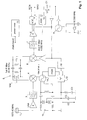
- a preferred embodiment of the invention is an RF-receiver shown in Fig. 1.
- the receiver shown here is used for receiving the signal of GPS satellites at 1575.42 MHz, but the same technique can be applied to other type of radio receivers, in particular for digital signals.
- the receiver comprises an antenna 1 with low noise amplifier 2 and an input filter 3.
- the signal from input filter 3 is fed to a frequency mixer 4, which mixes the carrier at 1575.42 MHz with a frequency of 1554.96 MHz to generate a downconverted first IF signal at 20.46 MHz.
- the first IF signal is filtered in a first IF filter 5 and fed to a second mixer 6, where it is mixed with a frequency of 16.368 MHz to generate a second downconverted IF signal at 4.092 MHz.
- the second IF signal is fed through a second IF filter 7 and to a adjustable amplifier 8.
- the output of adjustable amplifier 9 is fed to an A/D-converter 9 which generates a digital value of two bits SGN and MAG giving the sign and magnitude of the signal.
- the magnitude bit is analyzed by an adjustable gain control (AGC) 10 to set the gain of adjustable amplifier 8.
- AGC adjustable gain control
- AGC 10 The design of AGC 10 is shown in Fig. 2. It comprises a switch control unit 20 controlling a switch 21. In a first state, switch 21 connects a capacitor C1 via a current source 22 to the positive supply voltage Vdd. In a second state, switch 21 connects capacitor C1 via a current source 23 to the negative supply voltage or ground. In a thirds state, switch 23 is in high impedance state. The voltage U1 over C1 is fed as a control voltage to the high impedance input of a buffer 24, the output of which controls amplifier 8, wherein a lower voltage U1 corresponds to a higher amplification in amplifier 8.
- switch 21 In normal operation, if MAG is 1, switch 21 is in its first state and, if MAG is 0, switch 21 is in its second state, i.e. the voltage over capacitor C1 is proportional to the average value of MAG. If the average value of MAG is large, voltage U1 increases, thereby decreasing the amplification of adjustable amplifier 8 and vice versa. The gain loop is adjusted such that it tries to hold MAG at an average value of 0.33.
- the circuit of Fig. 1 further comprises a Quartz oscillator 11 operating at 16.368 MHz. It generates the reference frequency for second mixer 6. Furthermore, it provides a frequency base for a PLL.
- the PLL comprises a phase and frequency comparator 12 for comparing the Quartz oscillator frequency divided by 16 to the PLL's frequency divided by 1520.
- the output of comparator 12 is fed to a low pass filter comprising storage capacitors C2, C3, the voltage U2 over which is the control voltage for the resonance frequency of a tank circuit 13 of a VCO 14.
- the VCO's frequency is kept at 1554.96 MHz, the reference frequency for first mixer 4.
- Fig. 3 The design of the part of the PLL that drives capacitors C2, C3 is shown in Fig. 3. It comprises a switch control unit 26 controlling a switch 27. In a first state, switch 27 connects capacitors C2, C3 via a current source 29 to the positive supply voltage Vdd. In a second state, switch 27 connects capacitors C2, C3 via a current source 30 to the negative supply voltage or ground. In a third state, switch 27 is in high impedance state. If the comparator finds that the VCO's frequency is too low, switch 27 is primarily set to its first state, thereby increasing voltage U2 over the capacitors, while, if the VCO's frequency is too high and for decreasing voltage U2, switch 27 is primarily in its second state.
- the circuit of Fig. 1 comprises a power save unit 15.
- the purpose of this power save unit is to temporarily switch off the circuits of the RF receiver for conservation of power.
- the position and length of the switch-off periods can e.g. be selected according to a known temporal structure of the incoming signal or according to requirements of the user of the RF receiver.
- Power save unit 15 switches off power supply to mixers 4, 6, amplifiers 2, 8, ADC 9 and AGC 10, as well as to the PLL (comparator 12, VCO 14 and frequency dividers) by issuing a control signal PWR SAVE.
- Typical power-off periods may e.g. have a duration between 1 ms and several seconds.
- the start-up time of the receiver would be limited by the time it takes for the circuit to reestablish its dynamic settings. These settings are the amplification of adjustable amplifier 8 as well as the frequency of the PLL.
- the circuit of Fig. 1 is designed to store these settings as control voltages U1, U2 over the capacitors C1 and C2 or C3. While power is off, the load impedance offered by the circuits to these capacitors is high enough to make the discharge time of the capacitors much longer than a typical power-off period.
- a typical power-off period is e.g. limited by a few seconds, while the discharge time is e.g. 100 times as large.
- capacitors C1, C2 and C3 serve two purposes. First they act as low pass filters or integraters in their corresponding feed-back loops (ACG and PLL), second they store the setting of the loop during power-off.
- switches 21 and 27 are both set to their third, high impedance state while the signal PWR SAVE indicates that the circuit is switched off.
- the capacities of the capacitors can be increased where possible.
- active hold circuits can be used to maintain the voltage of the capacitors during power-off periods.
- the storage capacitor can e.g. be arranged in the negative feedback loop between the amplifier output and its inverting input.
- the circuit By storing the control voltages in the capacitors, the circuit can be switched back on quickly because its settings are maintained.
- the principle described here can be used in other electronic circuits having settings that can be controlled by control voltages.
- the control voltages can be stored in suitable capacitors while power is shut down.
- the technique shown here is especially suited for PLL circuits in any application or for storing the amplification setting or setpoint of an adjustable RF or LF amplifier. It can also be used for storing the settings of any feedback loops.
- power save unit 15 is controlled automatically, i.e. the time and duration of the switch-off periods are not directly determined by the user.
- power save unit 15 could also be controlled by the user directly.
Landscapes
- Engineering & Computer Science (AREA)
- Computer Networks & Wireless Communication (AREA)
- Signal Processing (AREA)
- Remote Sensing (AREA)
- Radar, Positioning & Navigation (AREA)
- Physics & Mathematics (AREA)
- General Physics & Mathematics (AREA)
- Circuits Of Receivers In General (AREA)
- Stabilization Of Oscillater, Synchronisation, Frequency Synthesizers (AREA)
- Control Of Amplification And Gain Control (AREA)
- Superheterodyne Receivers (AREA)
- Selective Calling Equipment (AREA)
- Burglar Alarm Systems (AREA)
- Power Conversion In General (AREA)
Abstract
Description
- The invention relates to an electronic circuit and a radio frequency receiver according to the preamble of the independent claims.
- It has been known to provide electronic circuits with power save units for switching the circuits off when they are not used. When switching the circuits off, it may be required or desirable that their settings are saved. E.g. when switching a TV off by a remote control, its current loudness settings should be preserved. For this purpose, a control voltage controlling the loudness is stored in a digital memory, from where it is fed to an D/A-converter when the device is switched back on. This, however, requires additional circuitry.
- Furthermore, it has been know to preserve energy in radio frequency receivers by switching the receiver section on and off, in particular in receivers of digital data with a know time structure. In such receivers, the settings of the receiver section, e.g. the control voltage of a VCO in a PLL, are usually lost during power-off periods. When these components are switched back on, some time passes before the settings have been re-established.
- Hence, the problem to be solved by the present invention is to provide an electronic circuit and an RF receiver of the type mentioned above that maintain their settings while being switched off without requiring additional complicated circuitry.
- This problem is solved by the independent claims.
- To store the setting, the corresponding control voltage is stored in a storage capacitor. This obviates the need for providing a digital memory and a D/A-converter. Since the control voltage needs not be converted to digital information and back, circuitry remains simple and power consumption is reduced.
- For a reliable storage of the control voltage, a discharge time of the capacitor during switch-off should be much larger than a typical switch-off time.
- To increase storage time, an electronic switch can be provided for disconnecting the capacitor from at least part of the circuit elements while they are switched off. Alternatively or in addition to that, an active hold circuit can be used for maintaining the voltage over the capacitor.
- The technology described here is particularly useful for RF receivers. When part of an RF receiver is switched off for reducing power consumption, its settings can be maintained using capacitive storage.
- In particular, RF receivers usually comprise down-converters, where the incoming signal is mixed to a reference frequency. The reference frequency is usually generated by a VCO in a PLL. If such a circuit is switched off and back on, it requires some time to regain stable reference frequency unless the voltage controlling the VCO is stored.
- Further preferred embodiments as well as applications of the invention are described in the dependent claims as well as in the following description making reference to the enclosed figures, wherein
- Fig. 1 shows a circuit diagram of an RF receiver,
- Fig. 2 part of the automatic gain control circuit, and
- Fig. 3 part of the PLL circuit.
-
- A preferred embodiment of the invention is an RF-receiver shown in Fig. 1. The receiver shown here is used for receiving the signal of GPS satellites at 1575.42 MHz, but the same technique can be applied to other type of radio receivers, in particular for digital signals.
- The receiver comprises an antenna 1 with
low noise amplifier 2 and an input filter 3. The signal from input filter 3 is fed to afrequency mixer 4, which mixes the carrier at 1575.42 MHz with a frequency of 1554.96 MHz to generate a downconverted first IF signal at 20.46 MHz. The first IF signal is filtered in afirst IF filter 5 and fed to a second mixer 6, where it is mixed with a frequency of 16.368 MHz to generate a second downconverted IF signal at 4.092 MHz. The second IF signal is fed through a second IF filter 7 and to aadjustable amplifier 8. The output ofadjustable amplifier 9 is fed to an A/D-converter 9 which generates a digital value of two bits SGN and MAG giving the sign and magnitude of the signal. The magnitude bit is analyzed by an adjustable gain control (AGC) 10 to set the gain ofadjustable amplifier 8. - The design of AGC 10 is shown in Fig. 2. It comprises a
switch control unit 20 controlling aswitch 21. In a first state,switch 21 connects a capacitor C1 via acurrent source 22 to the positive supply voltage Vdd. In a second state,switch 21 connects capacitor C1 via acurrent source 23 to the negative supply voltage or ground. In a thirds state,switch 23 is in high impedance state. The voltage U1 over C1 is fed as a control voltage to the high impedance input of abuffer 24, the output of which controlsamplifier 8, wherein a lower voltage U1 corresponds to a higher amplification inamplifier 8. - In normal operation, if MAG is 1,
switch 21 is in its first state and, if MAG is 0,switch 21 is in its second state, i.e. the voltage over capacitor C1 is proportional to the average value of MAG. If the average value of MAG is large, voltage U1 increases, thereby decreasing the amplification ofadjustable amplifier 8 and vice versa. The gain loop is adjusted such that it tries to hold MAG at an average value of 0.33. - The circuit of Fig. 1 further comprises a
Quartz oscillator 11 operating at 16.368 MHz. It generates the reference frequency for second mixer 6. Furthermore, it provides a frequency base for a PLL. The PLL comprises a phase andfrequency comparator 12 for comparing the Quartz oscillator frequency divided by 16 to the PLL's frequency divided by 1520. The output ofcomparator 12 is fed to a low pass filter comprising storage capacitors C2, C3, the voltage U2 over which is the control voltage for the resonance frequency of atank circuit 13 of aVCO 14. By this arrangement, the VCO's frequency is kept at 1554.96 MHz, the reference frequency forfirst mixer 4. - The design of the part of the PLL that drives capacitors C2, C3 is shown in Fig. 3. It comprises a
switch control unit 26 controlling aswitch 27. In a first state,switch 27 connects capacitors C2, C3 via acurrent source 29 to the positive supply voltage Vdd. In a second state,switch 27 connects capacitors C2, C3 via acurrent source 30 to the negative supply voltage or ground. In a third state,switch 27 is in high impedance state. If the comparator finds that the VCO's frequency is too low,switch 27 is primarily set to its first state, thereby increasing voltage U2 over the capacitors, while, if the VCO's frequency is too high and for decreasing voltage U2,switch 27 is primarily in its second state. - The circuit of Fig. 1 comprises a
power save unit 15. The purpose of this power save unit is to temporarily switch off the circuits of the RF receiver for conservation of power. The position and length of the switch-off periods can e.g. be selected according to a known temporal structure of the incoming signal or according to requirements of the user of the RF receiver. -
Power save unit 15 switches off power supply tomixers 4, 6,amplifiers comparator 12,VCO 14 and frequency dividers) by issuing a control signal PWR SAVE. Typical power-off periods may e.g. have a duration between 1 ms and several seconds. - After a power-off period, power to the circuits of the RF receiver is switched back on and the RF receiver should become operational quickly. Without special provisions, the start-up time of the receiver would be limited by the time it takes for the circuit to reestablish its dynamic settings. These settings are the amplification of
adjustable amplifier 8 as well as the frequency of the PLL. To reduce the start-up time, the circuit of Fig. 1 is designed to store these settings as control voltages U1, U2 over the capacitors C1 and C2 or C3. While power is off, the load impedance offered by the circuits to these capacitors is high enough to make the discharge time of the capacitors much longer than a typical power-off period. A typical power-off period is e.g. limited by a few seconds, while the discharge time is e.g. 100 times as large. - It must be noted that the capacitors C1, C2 and C3 serve two purposes. First they act as low pass filters or integraters in their corresponding feed-back loops (ACG and PLL), second they store the setting of the loop during power-off.
- To achieve high discharge times, switches 21 and 27 are both set to their third, high impedance state while the signal PWR SAVE indicates that the circuit is switched off.
- To reach even higher discharge times, the capacities of the capacitors can be increased where possible. In addition or alternatively to this, active hold circuits can be used to maintain the voltage of the capacitors during power-off periods. In such a circuit, the storage capacitor can e.g. be arranged in the negative feedback loop between the amplifier output and its inverting input.
- By storing the control voltages in the capacitors, the circuit can be switched back on quickly because its settings are maintained.
- The principle described here can be used in other electronic circuits having settings that can be controlled by control voltages. In such circuits, the control voltages can be stored in suitable capacitors while power is shut down. The technique shown here is especially suited for PLL circuits in any application or for storing the amplification setting or setpoint of an adjustable RF or LF amplifier. It can also be used for storing the settings of any feedback loops.
- In the embodiment described above, power save
unit 15 is controlled automatically, i.e. the time and duration of the switch-off periods are not directly determined by the user. However, power saveunit 15 could also be controlled by the user directly.
Claims (11)
- An electronic circuit comprisingcharacterized in that the storage comprises a storage capacitor (C1; C2, C3) storing the controlvoltage.circuit elements a setting of which is controlled by at least one control voltage (U1, U2),a power save unit (15) for switching off the circuit elements during power-off periods, anda storage for storing the control voltage (U1, U2) while the circuit elements are switched off,
- The electronic circuit of one of the preceding claims wherein the storage comprises an electronic switch (21, 27) for disconnecting the capacitor (C1; C2, C3) from at least part of the circuit elements while the circuit elements are switched off.
- The electronic circuit of one of the preceding claims wherein the storage comprises a hold circuit for actively maintaining the voltage over the capacitor (C1; C2, C3) while the circuit elements are switched off.
- The electronic circuit of one of the preceding claims comprising at least one amplifier (8), wherein an amplification factor of the amplifier (8) is controlled by the control voltage (U1).
- The electronic circuit of one of the preceding claims comprising at least one phase locked loop with a voltage controlled oscillator (13, 14), wherein the control voltage (U2) controls the frequency of the voltage controlled oscillator.
- The electronic circuit of one of the preceding claims wherein the power save unit (15) is adapted to switch off the circuit elements for a typical time period, wherein, during switch-off, a discharge time of the capacitor (C1; C2, C3) is much larger than the typical time period.
- The electronic circuit of one of the preceding claims wherein the capacitor (C1; C2, C3) is part of a low pass filter in a feed-back loop.
- A radio frequency receiver comprising the electronic circuit of one of the preceding claims.
- The radio frequency receiver of claim 8 comprising a frequency downconverter (4) for downconverting an incoming signal to an intermediate frequency and an oscillator circuit (14) being connected to the downconverter (4), wherein a frequency of the oscillator circuit (14) is being controlled by the control voltage and wherein the oscillator (14) is being switched on and off by the power save unit (15).
- The radio frequency receiver of claim 9 wherein the oscillator circuit comprises a voltage controlled oscillator (13, 14) in a phase locked loop, wherein the frequency of the voltage controlled oscillator (13, 14) is being controlled by the control voltage.
- The radio frequency receiver of one of the claims 8 - 10 wherein the power save unit (15) switches the electronic circuit on and off according to a temporal structure of a received radio signal.
Priority Applications (6)
| Application Number | Priority Date | Filing Date | Title |
|---|---|---|---|
| EP00810933A EP1198068B1 (en) | 2000-10-10 | 2000-10-10 | Electronic circuit and RF receiver with power save control |
| DE60038679T DE60038679T2 (en) | 2000-10-10 | 2000-10-10 | Electronic circuit and RF receiver with energy saving control |
| AT00810933T ATE393496T1 (en) | 2000-10-10 | 2000-10-10 | ELECTRONIC CIRCUIT AND RF RECEIVER WITH ENERGY SAVING CONTROL |
| CA002357499A CA2357499A1 (en) | 2000-10-10 | 2001-09-19 | Rf receiver with power off control |
| US09/973,593 US6968220B2 (en) | 2000-10-10 | 2001-10-09 | RF receiver with power off control |
| JP2001311180A JP3995440B2 (en) | 2000-10-10 | 2001-10-09 | Radio frequency receiver with power off control function |
Applications Claiming Priority (1)
| Application Number | Priority Date | Filing Date | Title |
|---|---|---|---|
| EP00810933A EP1198068B1 (en) | 2000-10-10 | 2000-10-10 | Electronic circuit and RF receiver with power save control |
Publications (2)
| Publication Number | Publication Date |
|---|---|
| EP1198068A1 true EP1198068A1 (en) | 2002-04-17 |
| EP1198068B1 EP1198068B1 (en) | 2008-04-23 |
Family
ID=8174962
Family Applications (1)
| Application Number | Title | Priority Date | Filing Date |
|---|---|---|---|
| EP00810933A Expired - Lifetime EP1198068B1 (en) | 2000-10-10 | 2000-10-10 | Electronic circuit and RF receiver with power save control |
Country Status (6)
| Country | Link |
|---|---|
| US (1) | US6968220B2 (en) |
| EP (1) | EP1198068B1 (en) |
| JP (1) | JP3995440B2 (en) |
| AT (1) | ATE393496T1 (en) |
| CA (1) | CA2357499A1 (en) |
| DE (1) | DE60038679T2 (en) |
Cited By (7)
| Publication number | Priority date | Publication date | Assignee | Title |
|---|---|---|---|---|
| WO2005003807A1 (en) | 2003-07-03 | 2005-01-13 | Nemerix Sa | Gps receiver with fast acquisition time |
| EP2066040A1 (en) | 2007-11-27 | 2009-06-03 | Nemerix SA | Multipath mitigation GNSS Receiver |
| US7551132B2 (en) * | 2004-07-02 | 2009-06-23 | Nemerix Sa | GPS receiver with fast acquisition time |
| US7696925B2 (en) | 2006-09-21 | 2010-04-13 | Qualcomm Incorporated | Memory reduction in GNSS receiver |
| US8406277B2 (en) | 2005-12-16 | 2013-03-26 | Qualcomm Incorporated | Signal processor and signal processing method |
| US8520717B2 (en) | 2006-10-26 | 2013-08-27 | Qualcomm Incorporated | GNSS receiver with cross-correlation rejection |
| US9151846B2 (en) | 2005-12-16 | 2015-10-06 | Qualcomm Incorporated | Signal processor and signal processing method |
Families Citing this family (10)
| Publication number | Priority date | Publication date | Assignee | Title |
|---|---|---|---|---|
| FI113817B (en) * | 2002-05-27 | 2004-06-15 | Nokia Corp | Enhanced Circuit Arrangement for Phase Lock, Integrated Circuit Implementing Phase Lock, Phase Lock Method and Cellular Network Terminal |
| US7184799B1 (en) | 2003-05-14 | 2007-02-27 | Marvell International Ltd. | Method and apparatus for reducing wake up time of a powered down device |
| US7724846B2 (en) * | 2003-06-05 | 2010-05-25 | Broadcom Corporation | Method and apparatus for mitigating interference in a satellite signal receiver |
| EP1664824B1 (en) * | 2003-09-02 | 2015-01-14 | SiRF Technology, Inc. | Satellite positioning receiver and method of communicating between the signal processing and FFT subsystems of said satellite positioning receiver |
| US20050176462A1 (en) * | 2004-02-06 | 2005-08-11 | Kenichi Kawasaki | Systems and methods for reducing power consumption in a receiver |
| US7283851B2 (en) * | 2004-04-05 | 2007-10-16 | Qualcomm Incorporated | Power saving mode for receiver circuit blocks based on transmitter activity |
| US7962362B2 (en) * | 2004-08-11 | 2011-06-14 | Canadian Bank Note Company, Limited | Promoting customer loyalty |
| US7522898B2 (en) * | 2005-06-01 | 2009-04-21 | Wilinx Corporation | High frequency synthesizer circuits and methods |
| IL180673A0 (en) * | 2007-01-11 | 2007-12-03 | Vadim Leibman | Low power radio frequency receiver |
| JP2014130118A (en) * | 2012-12-28 | 2014-07-10 | Fujitsu Mobile Communications Ltd | Communication device, switching program and switching method |
Citations (4)
| Publication number | Priority date | Publication date | Assignee | Title |
|---|---|---|---|---|
| US4380832A (en) * | 1980-07-31 | 1983-04-19 | Nippon Electric Co., Ltd. | Portable radio communication device having signal processing circuit with presetting function |
| US4631737A (en) * | 1984-12-06 | 1986-12-23 | Motorola, Inc. | Self biasing direct coupled data limiter |
| US4866261A (en) * | 1987-01-02 | 1989-09-12 | Motorola, Inc. | Data limiter having current controlled response time |
| US4929851A (en) * | 1989-01-23 | 1990-05-29 | Motorola, Inc. | Data limiter for a radio pager |
Family Cites Families (16)
| Publication number | Priority date | Publication date | Assignee | Title |
|---|---|---|---|---|
| PL89827B1 (en) * | 1974-05-06 | 1976-12-31 | ||
| JPS5652440U (en) * | 1979-09-29 | 1981-05-09 | ||
| US4521918A (en) * | 1980-11-10 | 1985-06-04 | General Electric Company | Battery saving frequency synthesizer arrangement |
| EP0052289B1 (en) * | 1980-11-14 | 1987-04-22 | Texas Instruments Deutschland Gmbh | Voltage follower amplifier |
| DE3303711C2 (en) * | 1983-02-04 | 1985-01-24 | Deutsche Thomson-Brandt Gmbh, 7730 Villingen-Schwenningen | Voting unit for telecommunications equipment |
| DE3347132C1 (en) * | 1983-12-27 | 1985-07-04 | Deutsche Thomson-Brandt Gmbh, 7730 Villingen-Schwenningen | Automatic adjustment system for a tuner of a television receiver |
| GB8830282D0 (en) * | 1988-12-28 | 1989-02-22 | Astec Int Ltd | The setting of electronic circuits |
| US4893094A (en) * | 1989-03-13 | 1990-01-09 | Motorola, Inc. | Frequency synthesizer with control of start-up battery saving operations |
| CH677298A5 (en) * | 1989-04-17 | 1991-04-30 | Koechler Erika Fa | Frequency synthesiser circuit for portable radio receiver - has switch interrupting voltage to frequency divider and phase detector for reduced battery requirement |
| US5128632A (en) * | 1991-05-16 | 1992-07-07 | Motorola, Inc. | Adaptive lock time controller for a frequency synthesizer and method therefor |
| US5448756A (en) * | 1992-07-02 | 1995-09-05 | Motorola, Inc. | High frequency battery saver for a radio receiver |
| US6223061B1 (en) * | 1997-07-25 | 2001-04-24 | Cleveland Medical Devices Inc. | Apparatus for low power radio communications |
| JP3119605B2 (en) * | 1997-10-28 | 2000-12-25 | 埼玉日本電気株式会社 | Wireless base station |
| JP3587346B2 (en) * | 1998-08-07 | 2004-11-10 | 松下電器産業株式会社 | Wireless communication device and transmission power control method in wireless communication device |
| DE19837204B4 (en) * | 1998-08-17 | 2006-06-08 | Telefonaktiebolaget Lm Ericsson (Publ) | Dead-time reduction in frequency jumps in multiband synthesis units |
| US6697436B1 (en) * | 1999-07-13 | 2004-02-24 | Pmc-Sierra, Inc. | Transmission antenna array system with predistortion |
-
2000
- 2000-10-10 DE DE60038679T patent/DE60038679T2/en not_active Expired - Lifetime
- 2000-10-10 AT AT00810933T patent/ATE393496T1/en not_active IP Right Cessation
- 2000-10-10 EP EP00810933A patent/EP1198068B1/en not_active Expired - Lifetime
-
2001
- 2001-09-19 CA CA002357499A patent/CA2357499A1/en not_active Abandoned
- 2001-10-09 JP JP2001311180A patent/JP3995440B2/en not_active Expired - Fee Related
- 2001-10-09 US US09/973,593 patent/US6968220B2/en not_active Expired - Fee Related
Patent Citations (4)
| Publication number | Priority date | Publication date | Assignee | Title |
|---|---|---|---|---|
| US4380832A (en) * | 1980-07-31 | 1983-04-19 | Nippon Electric Co., Ltd. | Portable radio communication device having signal processing circuit with presetting function |
| US4631737A (en) * | 1984-12-06 | 1986-12-23 | Motorola, Inc. | Self biasing direct coupled data limiter |
| US4866261A (en) * | 1987-01-02 | 1989-09-12 | Motorola, Inc. | Data limiter having current controlled response time |
| US4929851A (en) * | 1989-01-23 | 1990-05-29 | Motorola, Inc. | Data limiter for a radio pager |
Cited By (9)
| Publication number | Priority date | Publication date | Assignee | Title |
|---|---|---|---|---|
| WO2005003807A1 (en) | 2003-07-03 | 2005-01-13 | Nemerix Sa | Gps receiver with fast acquisition time |
| EP2290832A2 (en) | 2003-07-03 | 2011-03-02 | Qualcomm Incorporated | GPS receiver with fast acquisition time |
| US7551132B2 (en) * | 2004-07-02 | 2009-06-23 | Nemerix Sa | GPS receiver with fast acquisition time |
| US8406277B2 (en) | 2005-12-16 | 2013-03-26 | Qualcomm Incorporated | Signal processor and signal processing method |
| US9151846B2 (en) | 2005-12-16 | 2015-10-06 | Qualcomm Incorporated | Signal processor and signal processing method |
| US7696925B2 (en) | 2006-09-21 | 2010-04-13 | Qualcomm Incorporated | Memory reduction in GNSS receiver |
| US8362952B2 (en) | 2006-09-21 | 2013-01-29 | Qualcomm Incorporated | Memory reduction in GNSS receiver |
| US8520717B2 (en) | 2006-10-26 | 2013-08-27 | Qualcomm Incorporated | GNSS receiver with cross-correlation rejection |
| EP2066040A1 (en) | 2007-11-27 | 2009-06-03 | Nemerix SA | Multipath mitigation GNSS Receiver |
Also Published As
| Publication number | Publication date |
|---|---|
| US6968220B2 (en) | 2005-11-22 |
| DE60038679T2 (en) | 2009-05-07 |
| US20020077074A1 (en) | 2002-06-20 |
| ATE393496T1 (en) | 2008-05-15 |
| CA2357499A1 (en) | 2002-04-10 |
| JP3995440B2 (en) | 2007-10-24 |
| JP2002185347A (en) | 2002-06-28 |
| DE60038679D1 (en) | 2008-06-05 |
| EP1198068B1 (en) | 2008-04-23 |
Similar Documents
| Publication | Publication Date | Title |
|---|---|---|
| EP1198068B1 (en) | Electronic circuit and RF receiver with power save control | |
| EP1743418B1 (en) | Direct current offset correction systems and methods | |
| US6741127B2 (en) | High-frequency amplifier circuit and radio communication apparatus using same | |
| US8036619B2 (en) | Oscillator having controllable bias modes and power consumption | |
| US20100056097A1 (en) | Low power radio frequency receiver | |
| US8781539B1 (en) | Method and apparatus for reducing wake up time of a powered down device | |
| WO2006055792A1 (en) | Adjustable-bias vco | |
| US6788161B2 (en) | Integrated oscillator circuit that inhibits noise generated by biasing circuitry | |
| US20120142283A1 (en) | Wireless communication apparatus | |
| US9112508B2 (en) | Adaptive powered local oscillator generator circuit and related method | |
| JP2001036349A (en) | Pll detecting circuit | |
| JP2968592B2 (en) | Mobile phone | |
| US7486153B2 (en) | Circuit and method for controlling an oscillation loop | |
| US5483687A (en) | Operational transconductance amplifier track and hold system | |
| US5939911A (en) | Frequency prescaler method and apparatus responsive to low input drive levels | |
| JPH10256903A (en) | Pll circuit | |
| KR100575985B1 (en) | Apparatus and method for sleep mode control of direction conversion in a wireless communication system | |
| JP2010088086A (en) | Rf receiving circuit, gps receiver, and electronic apparatus | |
| KR100755595B1 (en) | Hybrid tuner | |
| JP2657137B2 (en) | Control unit for radio receiving circuit | |
| US10243602B2 (en) | Wireless receiver | |
| JP3744743B2 (en) | Tuner control semiconductor integrated circuit | |
| JP2000091845A (en) | Colpitts oscillating circuit and radio communication terminal equipment | |
| JPH08125561A (en) | Tuner | |
| JP2004274420A (en) | Front end for broadcast reception |
Legal Events
| Date | Code | Title | Description |
|---|---|---|---|
| PUAI | Public reference made under article 153(3) epc to a published international application that has entered the european phase |
Free format text: ORIGINAL CODE: 0009012 |
|
| AK | Designated contracting states |
Kind code of ref document: A1 Designated state(s): AT BE CH CY DE DK ES FI FR GB GR IE IT LI LU MC NL PT SE |
|
| AX | Request for extension of the european patent |
Free format text: AL;LT;LV;MK;RO;SI |
|
| 19U | Interruption of proceedings before grant |
Effective date: 20020529 |
|
| 19W | Proceedings resumed before grant after interruption of proceedings |
Effective date: 20040123 |
|
| RAP1 | Party data changed (applicant data changed or rights of an application transferred) |
Owner name: NEMERIX SA |
|
| AKX | Designation fees paid |
Designated state(s): AT BE CH CY DE DK ES FI FR GB GR IE IT LI LU MC NL PT SE |
|
| 17P | Request for examination filed |
Effective date: 20021017 |
|
| 17Q | First examination report despatched |
Effective date: 20060714 |
|
| GRAP | Despatch of communication of intention to grant a patent |
Free format text: ORIGINAL CODE: EPIDOSNIGR1 |
|
| GRAS | Grant fee paid |
Free format text: ORIGINAL CODE: EPIDOSNIGR3 |
|
| GRAA | (expected) grant |
Free format text: ORIGINAL CODE: 0009210 |
|
| AK | Designated contracting states |
Kind code of ref document: B1 Designated state(s): AT BE CH CY DE DK ES FI FR GB GR IE IT LI LU MC NL PT SE |
|
| REG | Reference to a national code |
Ref country code: GB Ref legal event code: FG4D |
|
| REG | Reference to a national code |
Ref country code: CH Ref legal event code: EP |
|
| REF | Corresponds to: |
Ref document number: 60038679 Country of ref document: DE Date of ref document: 20080605 Kind code of ref document: P |
|
| REG | Reference to a national code |
Ref country code: IE Ref legal event code: FG4D Free format text: LANGUAGE OF EP DOCUMENT: FRENCH |
|
| NLV1 | Nl: lapsed or annulled due to failure to fulfill the requirements of art. 29p and 29m of the patents act | ||
| PG25 | Lapsed in a contracting state [announced via postgrant information from national office to epo] |
Ref country code: FI Free format text: LAPSE BECAUSE OF FAILURE TO SUBMIT A TRANSLATION OF THE DESCRIPTION OR TO PAY THE FEE WITHIN THE PRESCRIBED TIME-LIMIT Effective date: 20080423 Ref country code: PT Free format text: LAPSE BECAUSE OF FAILURE TO SUBMIT A TRANSLATION OF THE DESCRIPTION OR TO PAY THE FEE WITHIN THE PRESCRIBED TIME-LIMIT Effective date: 20080923 Ref country code: NL Free format text: LAPSE BECAUSE OF FAILURE TO SUBMIT A TRANSLATION OF THE DESCRIPTION OR TO PAY THE FEE WITHIN THE PRESCRIBED TIME-LIMIT Effective date: 20080423 Ref country code: ES Free format text: LAPSE BECAUSE OF FAILURE TO SUBMIT A TRANSLATION OF THE DESCRIPTION OR TO PAY THE FEE WITHIN THE PRESCRIBED TIME-LIMIT Effective date: 20080803 |
|
| PG25 | Lapsed in a contracting state [announced via postgrant information from national office to epo] |
Ref country code: AT Free format text: LAPSE BECAUSE OF FAILURE TO SUBMIT A TRANSLATION OF THE DESCRIPTION OR TO PAY THE FEE WITHIN THE PRESCRIBED TIME-LIMIT Effective date: 20080423 |
|
| PG25 | Lapsed in a contracting state [announced via postgrant information from national office to epo] |
Ref country code: DK Free format text: LAPSE BECAUSE OF FAILURE TO SUBMIT A TRANSLATION OF THE DESCRIPTION OR TO PAY THE FEE WITHIN THE PRESCRIBED TIME-LIMIT Effective date: 20080423 Ref country code: SE Free format text: LAPSE BECAUSE OF FAILURE TO SUBMIT A TRANSLATION OF THE DESCRIPTION OR TO PAY THE FEE WITHIN THE PRESCRIBED TIME-LIMIT Effective date: 20080723 |
|
| ET | Fr: translation filed | ||
| PG25 | Lapsed in a contracting state [announced via postgrant information from national office to epo] |
Ref country code: BE Free format text: LAPSE BECAUSE OF FAILURE TO SUBMIT A TRANSLATION OF THE DESCRIPTION OR TO PAY THE FEE WITHIN THE PRESCRIBED TIME-LIMIT Effective date: 20080423 |
|
| PLBE | No opposition filed within time limit |
Free format text: ORIGINAL CODE: 0009261 |
|
| STAA | Information on the status of an ep patent application or granted ep patent |
Free format text: STATUS: NO OPPOSITION FILED WITHIN TIME LIMIT |
|
| 26N | No opposition filed |
Effective date: 20090126 |
|
| PG25 | Lapsed in a contracting state [announced via postgrant information from national office to epo] |
Ref country code: MC Free format text: LAPSE BECAUSE OF NON-PAYMENT OF DUE FEES Effective date: 20081031 |
|
| REG | Reference to a national code |
Ref country code: CH Ref legal event code: PL |
|
| PG25 | Lapsed in a contracting state [announced via postgrant information from national office to epo] |
Ref country code: IE Free format text: LAPSE BECAUSE OF NON-PAYMENT OF DUE FEES Effective date: 20081010 Ref country code: LI Free format text: LAPSE BECAUSE OF NON-PAYMENT OF DUE FEES Effective date: 20081031 Ref country code: CH Free format text: LAPSE BECAUSE OF NON-PAYMENT OF DUE FEES Effective date: 20081031 |
|
| REG | Reference to a national code |
Ref country code: FR Ref legal event code: TP |
|
| PG25 | Lapsed in a contracting state [announced via postgrant information from national office to epo] |
Ref country code: LU Free format text: LAPSE BECAUSE OF NON-PAYMENT OF DUE FEES Effective date: 20081010 Ref country code: CY Free format text: LAPSE BECAUSE OF FAILURE TO SUBMIT A TRANSLATION OF THE DESCRIPTION OR TO PAY THE FEE WITHIN THE PRESCRIBED TIME-LIMIT Effective date: 20080423 |
|
| PG25 | Lapsed in a contracting state [announced via postgrant information from national office to epo] |
Ref country code: GR Free format text: LAPSE BECAUSE OF FAILURE TO SUBMIT A TRANSLATION OF THE DESCRIPTION OR TO PAY THE FEE WITHIN THE PRESCRIBED TIME-LIMIT Effective date: 20080724 |
|
| PGFP | Annual fee paid to national office [announced via postgrant information from national office to epo] |
Ref country code: FR Payment date: 20101004 Year of fee payment: 11 |
|
| PGFP | Annual fee paid to national office [announced via postgrant information from national office to epo] |
Ref country code: GB Payment date: 20100923 Year of fee payment: 11 |
|
| PGFP | Annual fee paid to national office [announced via postgrant information from national office to epo] |
Ref country code: DE Payment date: 20101029 Year of fee payment: 11 |
|
| PGFP | Annual fee paid to national office [announced via postgrant information from national office to epo] |
Ref country code: IT Payment date: 20101021 Year of fee payment: 11 |
|
| GBPC | Gb: european patent ceased through non-payment of renewal fee |
Effective date: 20111010 |
|
| REG | Reference to a national code |
Ref country code: FR Ref legal event code: ST Effective date: 20120629 |
|
| PG25 | Lapsed in a contracting state [announced via postgrant information from national office to epo] |
Ref country code: DE Free format text: LAPSE BECAUSE OF NON-PAYMENT OF DUE FEES Effective date: 20120501 |
|
| REG | Reference to a national code |
Ref country code: DE Ref legal event code: R119 Ref document number: 60038679 Country of ref document: DE Effective date: 20120501 |
|
| PG25 | Lapsed in a contracting state [announced via postgrant information from national office to epo] |
Ref country code: IT Free format text: LAPSE BECAUSE OF NON-PAYMENT OF DUE FEES Effective date: 20111010 Ref country code: GB Free format text: LAPSE BECAUSE OF NON-PAYMENT OF DUE FEES Effective date: 20111010 Ref country code: FR Free format text: LAPSE BECAUSE OF NON-PAYMENT OF DUE FEES Effective date: 20111102 |