EP1198008A1 - Information processing structure - Google Patents
Information processing structure Download PDFInfo
- Publication number
- EP1198008A1 EP1198008A1 EP01915829A EP01915829A EP1198008A1 EP 1198008 A1 EP1198008 A1 EP 1198008A1 EP 01915829 A EP01915829 A EP 01915829A EP 01915829 A EP01915829 A EP 01915829A EP 1198008 A1 EP1198008 A1 EP 1198008A1
- Authority
- EP
- European Patent Office
- Prior art keywords
- quantum dots
- group
- information
- quantum dot
- charge carrier
- Prior art date
- Legal status (The legal status is an assumption and is not a legal conclusion. Google has not performed a legal analysis and makes no representation as to the accuracy of the status listed.)
- Withdrawn
Links
Images






Classifications
-
- H—ELECTRICITY
- H10—SEMICONDUCTOR DEVICES; ELECTRIC SOLID-STATE DEVICES NOT OTHERWISE PROVIDED FOR
- H10D—INORGANIC ELECTRIC SEMICONDUCTOR DEVICES
- H10D30/00—Field-effect transistors [FET]
- H10D30/60—Insulated-gate field-effect transistors [IGFET]
-
- B—PERFORMING OPERATIONS; TRANSPORTING
- B82—NANOTECHNOLOGY
- B82Y—SPECIFIC USES OR APPLICATIONS OF NANOSTRUCTURES; MEASUREMENT OR ANALYSIS OF NANOSTRUCTURES; MANUFACTURE OR TREATMENT OF NANOSTRUCTURES
- B82Y10/00—Nanotechnology for information processing, storage or transmission, e.g. quantum computing or single electron logic
-
- G—PHYSICS
- G11—INFORMATION STORAGE
- G11C—STATIC STORES
- G11C11/00—Digital stores characterised by the use of particular electric or magnetic storage elements; Storage elements therefor
- G11C11/21—Digital stores characterised by the use of particular electric or magnetic storage elements; Storage elements therefor using electric elements
- G11C11/34—Digital stores characterised by the use of particular electric or magnetic storage elements; Storage elements therefor using electric elements using semiconductor devices
-
- H—ELECTRICITY
- H10—SEMICONDUCTOR DEVICES; ELECTRIC SOLID-STATE DEVICES NOT OTHERWISE PROVIDED FOR
- H10D—INORGANIC ELECTRIC SEMICONDUCTOR DEVICES
- H10D30/00—Field-effect transistors [FET]
- H10D30/40—FETs having zero-dimensional [0D], one-dimensional [1D] or two-dimensional [2D] charge carrier gas channels
- H10D30/402—Single electron transistors; Coulomb blockade transistors
-
- H—ELECTRICITY
- H10—SEMICONDUCTOR DEVICES; ELECTRIC SOLID-STATE DEVICES NOT OTHERWISE PROVIDED FOR
- H10D—INORGANIC ELECTRIC SEMICONDUCTOR DEVICES
- H10D30/00—Field-effect transistors [FET]
- H10D30/60—Insulated-gate field-effect transistors [IGFET]
- H10D30/68—Floating-gate IGFETs
- H10D30/688—Floating-gate IGFETs programmed by two single electrons
-
- G—PHYSICS
- G11—INFORMATION STORAGE
- G11C—STATIC STORES
- G11C2216/00—Indexing scheme relating to G11C16/00 and subgroups, for features not directly covered by these groups
- G11C2216/02—Structural aspects of erasable programmable read-only memories
- G11C2216/08—Nonvolatile memory wherein data storage is accomplished by storing relatively few electrons in the storage layer, i.e. single electron memory
Definitions
- the present invention relates to an information processing structure for processing information by means of an electronic structure of a nanometer (nm) scale, for example from 10 nm to 0.3 nm and in particular to an information processing structure for detecting similarity of one pattern to another by way of single electron operations.
- nm nanometer
- quantum dots can be formed by the self-assembling formation in which silicon quantum dots are formed by low pressure CVD using mono-silane (see Mat. Res. Soc. Symp. Proc. 452 (1997) 243 “Self-Assembling Formation of Silicon Quantum Dots by Low Pressure Chemical Vapor Deposition”).
- Such an electronic device is commonly called a single electron device, and a variety of single electron circuits have been proposed by taking advantage of single electron devices.
- a complementary transistor akin to a CMOSFET it is possible to form as an electronic device a complementary transistor akin to a CMOSFET, and a single electron logic circuit using such a complementary transistor has already been proposed (See J. Appl. Phys., Vol. 72, No. 9, 1992, pp. 4399- 4413, J. R. Tucker: "Complementary Digital Logic Based on the Coulomb Blockade”).
- Hamming distance as an index to indicate similarity between digital patterns. This is defined by the number of those bits differing from each other of the digital patterns. Thus, it follows that the smaller the difference in the number of such different bits, the smaller the Hamming distance and the higher the similarity between the patterns, viz. more closely the patterns resemble each other.
- the Hamming distance can be computed, for example, by finding the exclusive ORs (XORs) of corresponding pairs of bits of the two digital patterns and summing those with the 1 output.
- a circuit as shown in Fig. 14(A) having a capacitor C 0 combined with a single electron transistor (hereinafter referred to as "SET") made up of a pair of tunnel junctions 1 and 2 exhibits a non-monotone characteristic as presented by the aforementioned Coulomb blockade phenomenon (See Applied Physics [a Japanese journal], Vol. 66, No. 2(1997), p. 100) and therefore, if supplied with voltages Va and Vb via capacitors at an intermediate point between the two tunnel junction 1 and 2, namely at its isolated node 3, exhibits a change with time dependence of its output voltage Vco as shown in Fig. 14(B) depending on a combination in H or L level of the input voltages Va and Vb.
- SET single electron transistor
- Fig. 15 shows a further single electron logic circuit in which a pair of SETs is connected parallel to each other between a power supply Vdd and a capacitor C 0 and to which inverted voltages of Va and Vb are also applied, thus providing a complementary structure.
- Such single electron logic circuits may be prepared in number equal to the number of bits of digital patterns to be compared with each other and may be connected to a common capacitor (C 0 ) to make up a bit comparator (BC) for the digital patterns as shown in Fig. 16 in which Va represents a bit voltage of one digital pattern to be compared and Vb represents a bit voltage of the other digital pattern to compare with.
- the tunneling phenomenon on the basis of which a single electron circuit operates is stochastic requires it to take fairly long before its operation is established, and makes the operation slow.
- the single electron logic circuit made by applying the architecture of a CMOS logic circuit must be slower in operation than, and hence fail to be superior to, the conventional CMOS logic circuit.
- the present invention is aimed to provide information processing structures formed of a plurality of single electron circuits each of which operates rapidly and stably by way of a single electron operation at a room temperature.
- an information processing structure having a MOSFET, and a plurality of quantum dots disposed immediately above a gate electrode of the MOSFET and each of which is made of a microconductor or microsemiconductor of a nanometer scale in size, wherein there is formed between each of the quantum dots and the gate electrode an energy barrier that a charge carrier consisting of either an electron or positive hole is capable of directly tunneling, and the total number of such charge carriers moved between the quantum dots and the gate electrode is used to represent information
- the structure comprises: a power source electrode disposed in contact with the said quantum dots; and at least a pair of information electrodes disposed across the said quantum dot in contact therewith for having electric potentials applied thereto, representing data of information, wherein there is formed between each of the said quantum dots and the said power source electrode a potential barrier that a said charge carrier is capable of tunneling, a capacitive coupling is provided between each of the said
- an information processing structure having a MOSFET, and a plurality of quantum dots of a first group formed immediately above a gate electrode of the MOSFET and each of which is made of a microconductor or microsemiconductor of a nanometer scale in size, wherein there is formed between each of the quantum dots of the first group and the gate electrode an energy barrier that a charge carrier consisting of either an electron or positive hole is capable of directly tunneling, and the total number of such charge carriers moved between the quantum dots of the first group and the gate electrode is used to represent information, wherein the structure comprises: a plurality of lines of quantum dots of a second group each of which lines has at least three quantum dots of the second group arranged in contact with a said quantum dot of the first group associated therewith but not in contact with the said gate electrode; and a plurality of pairs of information electrodes, the said information electrodes in each pair being disposed in contact with those quantum dots of the second group which are formed
- the said quantum dots of the first group are preferably arranged in a plurality of lines of quantum dots of the first group.
- a said information electrode is preferably formed by at least one quantum dot of a third group, and the number of charge carriers as aforesaid stored on such quantum dots of the third group is used to represent information.
- a second power source electrode is formed in contact with the information electrodes formed by the said quantum dots of the third group, there is formed between the said information electrode and the said second power source electrode an energy barrier that a said charge carrier is capable of directly tunneling, and a voltage or light energy applied to the said energy barrier makes a said charge carrier movable between the said information electrode and the said second power source electrode.
- an information processing structure that comprises: a line of quantum dots each of which is made of a microconductor or microsemiconductor and in which line there is formed between adjacent quantum dots an energy barrier that a charge carrier is capable of directly tunneling; a pair of information electrodes disposed across the said line of quantum dots and in contact with those quantum dots which are located at opposite ends of the said line of quantum dots, respectively, wherein there is provided a capacitive coupling between each of the said information electrodes and the said quantum dot located in contact therewith to prevent movement of a charge carrier between them; and a power source electrode formed in contact with that quantum dot which is located at a center of the said line of quantum dots, wherein there is provided a capacitive coupling between the said power source electrode and the said central quantum dot to prevent movement of a charge carrier between them, wherein the said power source electrode is adapted to have a voltage applied thereto so that the said quantum dots in the line has
- a plurality of single electron circuits each containing a plurality of quantum dots and a plurality of a pair of information electrode formed on the gate electrode of a MOSFET, and a power supply electrode thereof perform parallel information processing.
- the structure is capable of achieving a macroscopic information processing operation by putting together the processing results of these single electron circuits on the MOSFET. It can thus accomplish similarity computation for a multi-bit pattern on the single MOSFET.
- parallel operations by a plurality of quantum dots allows a redundancy configuration or majority logic to be utilized to control the influence of offset charges over the entire circuit system as much as practicable.
- the power source electrode and the information electrodes may be larger in size than the quantum dots and may thus be made up of a wiring pattern by the conventional lithographic method.
- An information processing structure of the second construction mentioned above is not only operable well as of the first construction, but also has the advantage that it can quantify the similarity (in terms of Hamming distance) more clearly as the number of electrons in a stable state.
- An information processing structure has the advantage that it is operable in a wider temperature range and operable even at a room temperature.
- a second power source electrode is formed in contact with the information electrodes formed by the quantum dots such that there is formed between each information electrode and the second power source electrode an energy barrier that a charge carrier is capable of directly tunneling, and a voltage or light energy applied to said energy barrier makes a charge carrier movable between the information electrode and the second power source electrode, it follows that the charge carrier is placed and held on the information electrode with the aid of the voltage or light energy, thus facilitating entry of data of information onto the information electrodes.
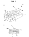
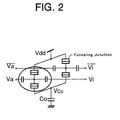
- Figs. 1 and 2 show the first form of embodiment of the information processing structure according to the present invention.
- the information processing structure designated by reference character 10 comprises a plurality of quantum dots 13 having a size of 10 nm to 0.3 nm and made up directly above a gate electrode 12 of a MOSFET 11, a power source electrode 14 formed above the quantum dots 13 so as to come from the above into contact therewith, and a like plurality of pairs of information electrodes 15 associated with the quantum dots 13, respectively, and formed so as to come in contact with the quantum dots 13 from their opposite sides, respectively.
- Each of these quantum dots 13 which are formed in a line along the gate electrode 12 is constituted from a micro-conductor or -semiconductor formed, e.g., by a method of self-assembling formation and corresponds to an isolated node of a SET.
- each quantum dot 13 makes a tunnel junction with the gate electrode 12.
- the gate capacitance of the MOSFET 11 corresponds to the aforementioned capacitance C 0 .
- the power source electrode 14 as illustrated is made in the form of a plate such as to come in contact with all the quantum dots 13 from the above and to make a tunnel junction with each of them. Further, the power source electrode 14 is supplied with a power supply voltage V dd .
- the information electrodes 15 are made of a first set of information electrode 15a (Va) each of which is positioned at one side of an adjacent quantum dot 13 and provided with an input pattern and a second set of information electrodes 15b (Vi) each of which is positioned at the other side of the adjacent quantum dot 13 and provided with a reference pattern, each of the information electrodes 15a and 15b being coupled with the quantum dot 13 between them in a capacitive coupling.
- information electrodes 15 in the form of embodiment illustrated are made in the form of a wiring pattern formed by lithography, they may be made up by quantum dots stored with electric charges.
- the information electrodes 15 may have the wiring pattern made thicker in size than the quantum dots 13, or the quantum dots corresponding to the information electrodes 15 may be made greater.
- a pair of quantum dots 13 together with two pairs of information electrodes 15a and 15b is designed to make up a pair of SETs whose equivalent circuit is shown in Fig. 2.
- the information processing structure 10 is made operable to perform information processing as is the single electron logic circuit shown in Fig. 15 by having, for each pair of SETs, one pair of information electrodes 15a and 15b supplied with input voltages Va and Vi for each bit of two digital patterns to be compared with each other and the other pair of information electrodes 15a and 15b supplied with inverting voltages Va and Vi.
- the result is a rise in the electric potential of the capacitor Vc 0 , which further can be taken out as a drain current of the MOSFET.
- the Hamming distance can indirectly be determined by comparison of the rate of such rise
- the SET pairs each of which requires only an extremely low power consumption and which can be integrated at an extremely high density makes the circuit operable as a whole to process information rapidly by having their super-parallel operation.
- the parallel operation of a plurality of quantum dots 13 permits the use of their redundancy configuration and majority logic to limit the influence of offset charges to possible minimum in the circuit as a whole.
- the power source electrode 14 can be made as a wiring by the conventional method, e.g., of lithography, and this makes it possible to form a parallel or redundancy configuration more simply and at a reduced cost.
- the ability of the information electrodes 15 if made by quantum dots to hold electrons and hence themselves to store information makes it unnecessary to provide them with any additional information storing means.
- the information processing structure designated by reference character 20 comprises a plurality of quantum dots 13 made up in a line on a gate electrode 12 of a MOSFET 11, a like plurality of rows 21 of quantum dots 21a of a second group, each row 21 having three such quantum dots 21a, made up above the quantum dots 13 so each row of quantum dots 21a come into contact with an adjacent one of the quantum dots 13 from the above, a power source electrode 14 formed above the rows 21 of quantum dot of the second group 21a so as to come into contact with thereto from the above, and a like plurality of pairs of quantum dots 22 formed as information electrodes for the rows 21 of the quantum dots of the second 21a, respectively, and formed so as to come in contact with those quantum dots of the second group 21a located at the opposite ends of their rows from their opposite sides, respectively.
- a tunnel junctions is made between each adjacent pair of quantum dots 21a of the second group in each of the rows 21, and a capacitive coupling is provided between each of those quantum dots of the second group 21a located at the opposite ends of each if the rows 21 and its counterpart information electrode 22 and so is between each of the quantum dots 21 of the second group and the power source electrode 14.
- Each pair of information electrodes 22 is provided across each corresponding row 21 of the three quantum dots of the second group 21a, respectively, and each of the information electrodes 22 is itself formed from a quantum dot.
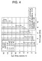
- Fig. 4 shows a range of values of capacitance C 0 required for a single electron logic circuit in this information processing structure to operate, which values are computed according to the Monte Carlo simulation method using a parasitic capacitance between the quantum dots as a parameter. Since even a capacitance C 0 of 10 -15 F makes the circuit operable as shown in Fig. 4, it will be seen that for the MOSFT 11 use may possibly be made of a fine MOSFET having a gate length in the order of 10 nm.
- a single quantum dot 13 in combination with a set as a row 21 of quantum dots of the second group 21a and a pair of information electrodes 22 makes up a single electron circuit whose equivalent circuit is shown in Fig. 5.
- an electron e M is placed on a quantum dot of the second class 21a (the central quantum dot 21a as shown) in the row 21 as shown in Fig. 6.
- This can be achieved by applying a high voltage to the power source electrode 14 to supply the quantum dot 21a with an electron, for example, by utilizing the Fowler-Nordheim tunneling phenomenon.
- the row 21 of quantum dots may have at its outside a second power source electrode (not shown) capacitively coupled thereto to which a high voltage can be applied to supply the quantum dot 21a with an electron likewise by utilizing the Fowler-Nordheim tunneling phenomenon.
- that portion of the second electrode may also be irradiated with a light to cause the electron to tunnel with the aid of light energy.
- the electron e M will come off the central quantum dot 21a, moving to the quantum dot 21 at either end of the row (as shown, at its left hand side end) to stabilize there.
- the electrons e M moved in response to the electric potentials at the two information electrodes 22 can be detected from the electrons e R placed on the quantum dot 13.
- the information processing structure 20 provides a bit comparator, namely an exclusive OR (XOR).
- XOR exclusive OR
- a plurality of bit such comparators can be connected together for the capacitor C 0 in common to store on the capacitor C 0 a number of electrons depending on a Hamming distance and to draw them as a drain current of the MOSFET.
- the Hamming distance can be expressed accurately as it is detected as a number of electrons on the capacitor C 0 in its stable state.
- the quantum dot 13 on which the electrons e R moved to the capacitor C 0 were initially positioned can be initialized by applying a bias voltage adjustably to the quantum dot 13 to return those electrons e R thereto.
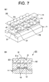
- a single quantum dot 13 is disposed in opposition to the central second quantum dot 21a in the row 21 of quantum dots
- two quantum dots 13 may be disposed in opposition respectively to the second quantum dots at the both ends of the row 21 of quantum dots of which the central second quantum dot 21a has electrons e M placed thereon.
- the electron e M moved in response to the different electric potentials at the two information electrodes 22 can be detected from electrons e R placed on the quantum dots 13.
- the information processing structure 20 here again provides a bit comparator, namely an inhibit exclusive NOR (XNOR).
- XNOR inhibit exclusive NOR
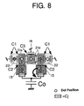
- Figs. 9 to 13 show the third form of embodiment of the information processing structure according to the present invention.
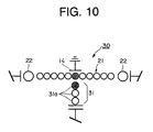
- the information processing structure designated by reference character 30 differs from the information processing structure 20 shown in Fig. 3 in that the second quantum dots 21a that make up the row 21 of quantum dots are increased in number to, e.g., eleven (11), that one quantum dot 13 is replaced by a row 31 of three quantum dots 31a, and that the central second quantum dot 21a in the row 21 of quantum dots is connected via a capacitive coupling to the ground.
- This construction of the information processing structure 30 is diagrammatically illustrated as in Fig. 10 indicating the quantum dots, the distances between the quantum dots and the distances between the quantum dots and electrodes.
- the electron when observed in a give time range near the room temperature, it is found that if the information electrodes 22 and 22 are identical to each other in electric potential, the electron will be located at the central quantum dot in the row of quantum dots and that if these information electrodes differ from each other in electric potential the electron will be located at the quantum dot at either end of the row of quantum dots.
- a plurality of such a structure constructed as shown in Fig. 9 can be connected together for the capacitor C 0 in common to store on the capacitor C 0 a number of electrons depending on a Hamming distance and to draw them as a drain current of the MOSFET.
- the information processing structure 30 having a row of quantum dots 21 made up of a larger number of quantum dots 21a permits a stochastic operation taking advantage of thermal fluctuation and is thus operable enough at a room temperature.
- charge carriers movable according to electric potentials of information electrodes are described as electrons, it is obvious that they are not limited so but may be positive holes as well.
- the present invention provides an information processing structure in which a plurality of single electron circuits each containing a plurality of quantum dots formed on the gate electrode of a MOSFET and each of 10 nm to 0.3 nm in size perform parallel information processing.
- the structure With each of the single electron circuits taking out its processing result as a drain current on the MOSFET, the structure is capable of achieving a macroscopic information processing operation by putting together the processing results of these single electron circuits on the MOSFET. It can thus accomplish similarity computation for a multi-bit pattern on the single MOSFET.
- An information processing structure according to the present invention described as the first form of embodiment thereof has the advantage that it can compare patterns with each other as to their similarity in a simple construction.
- An information processing structure according to the present invention described as the second form of embodiment thereof has the advantage that though less simple than the first it can quantify the similarity (in terms of Hamming distance) more clearly as the number of electrons in a stable state.
- an information processing structure according to the present invention described as the third form of embodiment thereof has the advantage that it is operable in a wider temperature range and operable even at a room temperature.
- an information processing structure according to the present invention is applicable to a device that executes information processing by utilizing pattern's similarity, to an intelligent processing or learning machines based on neural networks, and further to an associative processor or the like.
Landscapes
- Engineering & Computer Science (AREA)
- Chemical & Material Sciences (AREA)
- Nanotechnology (AREA)
- Physics & Mathematics (AREA)
- Mathematical Physics (AREA)
- Theoretical Computer Science (AREA)
- Crystallography & Structural Chemistry (AREA)
- Computer Hardware Design (AREA)
- Semiconductor Memories (AREA)
- Insulated Gate Type Field-Effect Transistor (AREA)
- Junction Field-Effect Transistors (AREA)
- Non-Volatile Memory (AREA)
Abstract
Description
Claims (7)
- An information processing structure having a MOSFET, and a plurality of quantum dots disposed immediately above a gate electrode of the MOSFET and each of which is made of a microconductor or microsemiconductor of a nanometer scale, wherein there is formed between each of the quantum dots and the gate electrode an energy barrier that a charge carrier consisting of either an electron or positive hole is capable of directly tunneling, and the total number of such charge carriers moved between the quantum dots and the gate electrode is used to represent information, characterized in that the structure comprises:a power source electrode disposed in contact with said quantum dots; andat least a pair of information electrodes disposed across a said quantum dot in contact therewith for having electric potentials applied thereto, representing data of information, whereinthere is formed between each of said quantum dots and said power source electrode a potential barrier that a said charge carrier is capable of tunneling,a capacitive coupling is provided between said information electrodes in pair and the quantum dot between them to prevent movement of a said charge carrier between said quantum dot and said information electrodes, anda said charge carrier is rendered movable by the Coulomb blockade through said quantum dot between said power source electrode and said gate electrode in response to a relative electric potential determined at said information electrodes.
- An information processing structure having a MOSFET, and a plurality of quantum dots of a first group formed immediately above a gate electrode of the MOSFET and each of which is made of a microconductor or microsemiconductor of a nanometer scale in size, wherein there is formed between each of the quantum dots of the first group and the gate electrode an energy barrier that a charge carrier consisting of either an electron or positive hole is capable of directly tunneling, and the total number of such charge carriers moved between the quantum dots of the first group and the gate electrode is used to represent information, characterized in that the structure comprises:a plurality of lines of quantum dots of a second group each of which lines has at least three or more quantum dots of the second group arranged in contact with a said quantum dot of the first group associated therewith but not in contact with said gate electrode and each of which quantum dots is made of a microconductor or microsemiconductor; anda plurality of pairs of information electrodes, said information electrodes in each pair being disposed in contact with those quantum dots of the second group which are formed at opposite ends of each of said lines, respectively, for having electric potentials applied thereto representing data of information, whereina capacitive coupling is provided each between said quantum dot of the first group and said quantum dots of the second group in each of said lines, and between said quantum dots of the second group in each such line and each of said information electrodes in each pair corresponding thereto to prevent movement of a said charge carrier each between them, anda change caused in position distribution of a said charge carrier in said quantum dots of the second group in each such line in response to a relative electric potential determined at said information electrodes in the pair corresponding thereto makes a said charge carrier movable between said quantum dot of the first group and said gate electrode.
- An information processing structure as set forth in claim 2, characterized in that said quantum dots of the first group are arranged in a plurality of lines of quantum dots, and there is formed between adjacent quantum dots in each of said lines an energy barrier that a said charge carrier is capable of directly tunneling.
- An information processing structure as set forth in any one of claim 1 to 3, characterized in that a said information electrode is formed by at least one quantum dot of a third group made of a microconductor or microsemiconductor, and the number of charge carriers as aforesaid stored on such quantum dots of the third group is used to represent information.
- An information processing structure as set forth in any one of claim 1 to 4, characterized in that in contact with the information electrodes formed by said quantum dots of the third group a second power source electrode is formed, there is formed between a said information electrode and said second power source electrode an energy barrier that a said charge carrier is capable of directly tunneling, and a voltage or light energy applied to said energy barrier makes the charge carrier movable between said information electrode and said second power source electrode.
- An information processing structure, characterized in that it comprises:wherein said power source electrode is adapted to have a voltage applied thereto so that said quantum dots in the line of the first group has a potential distribution such that a potential valley is formed about said central quantum dot of the first group, anda line of quantum dots of a first group each of which is made of a microconductor or microsemiconductor and in which line there is formed between adjacent quantum dots an energy barrier that a charge carrier is capable of directly tunneling;at least a pair of information electrodes of a first group disposed across said line of quantum dots of the first group and in contact with those quantum dots which are located at opposite ends of said line of quantum dots, respectively, wherein there is provided a capacitive coupling between each of said information electrodes in each pair and said quantum dot located in contact therewith to prevent movement of a charge carrier between them;a power source electrode formed in contact with that quantum dot of the first group, which is located at a center of said line of quantum dots, wherein there is provided a capacitive coupling between said power source electrode and said central quantum dot to prevent movement of a charge carrier between them;a line of quantum dots of a second group each of which is made of a microconductor or microsemiconductor and one end of which line of quantum dots is disposed in contact with said central quantum dot of the first group; andan information electrode of a second group formed at the other end of said line of quantum dots of the second group, wherein there is formed each between adjacent quantum dots of the second group, and between said line of quantum dots of the second group and said information electrode of the second group an energy barrier that a charge carrier is capable of directly tunneling, and there is provided a capacitive coupling between said central quantum dot of the first group and the quantum dot of the second group located at said one end to prevent movement of a charge carrier each between them,
wherein a charge carrier placed on said central quantum dot in the line of the first group is either immobile, or movable according to thermal fluctuation to one of the information electrode in the pair, depending upon a potential distribution determined by relative voltages at said information electrodes of the first class. - An information processing structure as set forth in claim 6, characterized in that said second information electrode comprises the gate electrode of a MOSFET.
Applications Claiming Priority (3)
| Application Number | Priority Date | Filing Date | Title |
|---|---|---|---|
| JP2000131633 | 2000-04-28 | ||
| JP2000131633A JP4873335B2 (en) | 2000-04-28 | 2000-04-28 | Information processing structure |
| PCT/JP2001/002469 WO2001084634A1 (en) | 2000-04-28 | 2001-03-27 | Information processing structure |
Publications (2)
| Publication Number | Publication Date |
|---|---|
| EP1198008A1 true EP1198008A1 (en) | 2002-04-17 |
| EP1198008A4 EP1198008A4 (en) | 2003-10-01 |
Family
ID=18640498
Family Applications (1)
| Application Number | Title | Priority Date | Filing Date |
|---|---|---|---|
| EP01915829A Withdrawn EP1198008A4 (en) | 2000-04-28 | 2001-03-27 | INFORMATION PROCESSING STRUCTURE |
Country Status (7)
| Country | Link |
|---|---|
| US (1) | US6661022B2 (en) |
| EP (1) | EP1198008A4 (en) |
| JP (1) | JP4873335B2 (en) |
| KR (1) | KR100524102B1 (en) |
| CN (3) | CN100364106C (en) |
| TW (1) | TW508821B (en) |
| WO (1) | WO2001084634A1 (en) |
Cited By (4)
| Publication number | Priority date | Publication date | Assignee | Title |
|---|---|---|---|---|
| US7493353B2 (en) | 2002-07-22 | 2009-02-17 | Panasonic Corporation | Stochastic processor, driving method thereof, and recognition process device using the same |
| US7936500B2 (en) | 2007-03-02 | 2011-05-03 | Ravenbrick Llc | Wavelength-specific optical switch |
| US8363307B2 (en) | 2007-02-28 | 2013-01-29 | Ravenbrick, Llc | Multicolor light emitting device incorporating tunable quantum confinement devices |
| WO2017182826A1 (en) * | 2016-04-22 | 2017-10-26 | Oxford University Innovation Limited | Coupled quantum dot memristor |
Families Citing this family (37)
| Publication number | Priority date | Publication date | Assignee | Title |
|---|---|---|---|---|
| US20020091114A1 (en) | 2000-10-04 | 2002-07-11 | Odile Piot-Grosjean | Combination of a CB1 receptor antagonist and of sibutramine, the pharmaceutical compositions comprising them and their use in the treatment of obesity |
| JP3545743B2 (en) * | 2001-12-13 | 2004-07-21 | 株式会社東芝 | Feature extraction system and semiconductor integrated circuit device |
| JP3974429B2 (en) * | 2002-02-28 | 2007-09-12 | 株式会社東芝 | Random number generator |
| US6992899B2 (en) * | 2003-03-21 | 2006-01-31 | Intel Corporation | Power delivery apparatus, systems, and methods |
| WO2005020139A1 (en) * | 2003-08-20 | 2005-03-03 | Qucor Pty Ltd | Buried quantum device |
| JP4146395B2 (en) * | 2004-06-09 | 2008-09-10 | 株式会社東芝 | Storage device |
| US7397277B2 (en) * | 2005-10-17 | 2008-07-08 | Northern Lights Semiconductor Corp. | Magnetic transistor circuit with the EXOR function |
| US7601946B2 (en) * | 2006-09-12 | 2009-10-13 | Ravenbrick, Llc | Electromagnetic sensor incorporating quantum confinement structures |
| CN100468748C (en) * | 2006-11-01 | 2009-03-11 | 中国科学院半导体研究所 | A silicon-based single-electron memory with side gate structure and its manufacturing method |
| EP2106560B1 (en) | 2007-01-24 | 2017-04-26 | Ravenbrick, LLC | Thermally switched optical downconverting filter |
| JP2008288346A (en) * | 2007-05-16 | 2008-11-27 | Hiroshima Univ | Semiconductor element |
| US7755829B2 (en) | 2007-07-11 | 2010-07-13 | Ravenbrick Llc | Thermally switched reflective optical shutter |
| EP2195689A4 (en) | 2007-09-19 | 2012-05-02 | Ravenbrick Llc | LOW EMISSIVITY WINDOW FILMS AND COATINGS INCORPORATING NANOSCALE SCALE WIRE GRIDS |
| US8169685B2 (en) | 2007-12-20 | 2012-05-01 | Ravenbrick, Llc | Thermally switched absorptive window shutter |
| JP5671449B2 (en) | 2008-04-23 | 2015-02-18 | レイブンブリック,エルエルシー | Method and apparatus for adjusting glare for reflective and thermoreflective surfaces |
| EP2308111B1 (en) | 2008-06-17 | 2021-04-28 | National Research Council Of Canada | Atomistic quantum dots |
| US9116302B2 (en) | 2008-06-19 | 2015-08-25 | Ravenbrick Llc | Optical metapolarizer device |
| CN102187262B (en) | 2008-08-20 | 2013-06-19 | 雷文布里克有限责任公司 | Methods for fabricating thermochromic filters |
| TW201032340A (en) * | 2009-02-26 | 2010-09-01 | Nat Applied Res Laboratories | A silicon quantum dot near-infrared phototransistor detector |
| KR101787767B1 (en) | 2009-04-10 | 2017-10-18 | 라벤브릭 엘엘씨 | Thermally switched optical filter incorporating a guest-host architecture |
| WO2011053853A2 (en) * | 2009-10-30 | 2011-05-05 | Ravenbrick Llc | Thermochromic filters and stopband filters for use with same |
| WO2011062708A2 (en) | 2009-11-17 | 2011-05-26 | Ravenbrick Llc | Thermally switched optical filter incorporating a refractive optical structure |
| EP2553520B1 (en) | 2010-03-29 | 2019-07-31 | Ravenbrick, LLC | Polymer-stabilized thermotropic liquid crystal device |
| WO2011153214A2 (en) | 2010-06-01 | 2011-12-08 | Ravenbrick Llc | Multifunctional building component |
| EP2580714B1 (en) * | 2010-06-11 | 2020-02-12 | Touchcode Technologies, LLC | System comprising a capacitive information carrier for acquiring information |
| EP2635996B1 (en) * | 2010-09-20 | 2017-11-08 | T-Touch International S.à.r.l. | Information carrier and system for acquiring information |
| WO2012158791A2 (en) * | 2011-05-16 | 2012-11-22 | The Board Of Trustees Of The University Of Illinois | Electronic device from dissipative quantum dots |
| WO2013033608A2 (en) | 2011-09-01 | 2013-03-07 | Wil Mccarthy | Thermotropic optical shutter incorporating coatable polarizers |
| US9748356B2 (en) | 2012-09-25 | 2017-08-29 | Stmicroelectronics, Inc. | Threshold adjustment for quantum dot array devices with metal source and drain |
| US9601630B2 (en) | 2012-09-25 | 2017-03-21 | Stmicroelectronics, Inc. | Transistors incorporating metal quantum dots into doped source and drain regions |
| EP2991118B1 (en) * | 2013-03-09 | 2023-02-22 | Japan Science and Technology Agency | Method of controlling a logical operation element |
| US10002938B2 (en) | 2013-08-20 | 2018-06-19 | Stmicroelectronics, Inc. | Atomic layer deposition of selected molecular clusters |
| JP6985993B2 (en) * | 2018-07-13 | 2021-12-22 | 株式会社日立製作所 | Learning method of electronic circuit and neural network using it |
| US11983126B2 (en) * | 2019-09-20 | 2024-05-14 | Rheinisch-Westfälische Technische Hochschule (Rwth) Aachen | Component for reading out the states of qubits in quantum dots |
| JP2021082130A (en) * | 2019-11-21 | 2021-05-27 | 株式会社日立製作所 | Electronic circuit, neural network, and learning method of neural network |
| JP7830245B2 (en) * | 2022-06-17 | 2026-03-16 | 株式会社日立製作所 | Quantum computer and its control method |
| US12249748B2 (en) | 2022-09-23 | 2025-03-11 | International Business Machines Corporation | Edge capacitive coupling for quantum chips |
Family Cites Families (9)
| Publication number | Priority date | Publication date | Assignee | Title |
|---|---|---|---|---|
| EP0441156B1 (en) * | 1990-01-23 | 1996-01-03 | Max-Planck-Gesellschaft zur Förderung der Wissenschaften e.V. | Electron-wave coupled semiconductor switching device |
| US5677637A (en) * | 1992-03-25 | 1997-10-14 | Hitachi, Ltd. | Logic device using single electron coulomb blockade techniques |
| JPH0786615A (en) * | 1993-09-14 | 1995-03-31 | Fujitsu Ltd | Semiconductor quantum dot device |
| US5951711A (en) * | 1993-12-30 | 1999-09-14 | Texas Instruments Incorporated | Method and device for determining hamming distance between two multi-bit digital words |
| US5838021A (en) * | 1995-12-26 | 1998-11-17 | Ancona; Mario G. | Single electron digital circuits |
| JPH10173181A (en) * | 1996-12-12 | 1998-06-26 | Sony Corp | Electronic element |
| JPH10256547A (en) * | 1997-03-17 | 1998-09-25 | Toshiba Corp | Semiconductor device |
| JP3769120B2 (en) * | 1998-05-08 | 2006-04-19 | 株式会社東芝 | Semiconductor element |
| JP3743745B2 (en) * | 1998-08-31 | 2006-02-08 | 株式会社東芝 | Semiconductor element |
-
2000
- 2000-04-28 JP JP2000131633A patent/JP4873335B2/en not_active Expired - Fee Related
-
2001
- 2001-03-27 EP EP01915829A patent/EP1198008A4/en not_active Withdrawn
- 2001-03-27 WO PCT/JP2001/002469 patent/WO2001084634A1/en not_active Ceased
- 2001-03-27 KR KR10-2001-7015560A patent/KR100524102B1/en not_active Expired - Fee Related
- 2001-03-27 CN CNB2004100685217A patent/CN100364106C/en not_active Expired - Fee Related
- 2001-03-27 US US09/926,698 patent/US6661022B2/en not_active Expired - Fee Related
- 2001-03-27 CN CNB2004100685221A patent/CN100373631C/en not_active Expired - Fee Related
- 2001-03-27 CN CNB018011268A patent/CN1197167C/en not_active Expired - Fee Related
- 2001-04-25 TW TW090109862A patent/TW508821B/en not_active IP Right Cessation
Cited By (5)
| Publication number | Priority date | Publication date | Assignee | Title |
|---|---|---|---|---|
| US7493353B2 (en) | 2002-07-22 | 2009-02-17 | Panasonic Corporation | Stochastic processor, driving method thereof, and recognition process device using the same |
| US8363307B2 (en) | 2007-02-28 | 2013-01-29 | Ravenbrick, Llc | Multicolor light emitting device incorporating tunable quantum confinement devices |
| US7936500B2 (en) | 2007-03-02 | 2011-05-03 | Ravenbrick Llc | Wavelength-specific optical switch |
| WO2017182826A1 (en) * | 2016-04-22 | 2017-10-26 | Oxford University Innovation Limited | Coupled quantum dot memristor |
| US10510956B2 (en) | 2016-04-22 | 2019-12-17 | Oxford University Innovation Limited | Coupled quantum dot memristor |
Also Published As
| Publication number | Publication date |
|---|---|
| CN1604337A (en) | 2005-04-06 |
| JP4873335B2 (en) | 2012-02-08 |
| CN1366712A (en) | 2002-08-28 |
| CN1604336A (en) | 2005-04-06 |
| KR100524102B1 (en) | 2005-10-26 |
| KR20020025886A (en) | 2002-04-04 |
| WO2001084634A1 (en) | 2001-11-08 |
| CN100364106C (en) | 2008-01-23 |
| TW508821B (en) | 2002-11-01 |
| EP1198008A4 (en) | 2003-10-01 |
| US20020134996A1 (en) | 2002-09-26 |
| CN100373631C (en) | 2008-03-05 |
| JP2001313386A (en) | 2001-11-09 |
| CN1197167C (en) | 2005-04-13 |
| US6661022B2 (en) | 2003-12-09 |
Similar Documents
| Publication | Publication Date | Title |
|---|---|---|
| US6661022B2 (en) | Information processing structures | |
| Porod et al. | Quantum-dot cellular automata: computing with coupled quantum dots | |
| Orlov et al. | Experimental demonstration of clocked single-electron switching in quantum-dot cellular automata | |
| Heij et al. | Negative differential resistance due to single-electron switching | |
| Hollenberg et al. | Charge-based quantum computing using single donors in semiconductors | |
| Amlani et al. | Demonstration of a six-dot quantum cellular automata system | |
| CA3027982A1 (en) | Electronic circuit for control or coupling of single charges or spins and methods therefor | |
| US5677637A (en) | Logic device using single electron coulomb blockade techniques | |
| Müller et al. | Effects of disorder on the blockade voltage of two-dimensional quantum dot arrays | |
| KR100435924B1 (en) | Single-electron memory cell arrangement | |
| WO1994015340A1 (en) | Memory device | |
| van Roermund et al. | Design philosophy for nanoelectronic systems, from sets to neural nets | |
| JP4438286B2 (en) | Quantum computing element and method of using the same | |
| Tanamoto | One-and two-dimensional N-qubit systems in capacitively coupled quantum dots | |
| US6307422B1 (en) | Circuit configuration having single-electron components, a method for its operation and use of the method for addition of binary numbers | |
| Orlov et al. | Experimental studies of quantum-dot cellular automata devices | |
| Khalafalla et al. | Identifying single-electron charging islands in a two-dimensional network of nanocrystalline silicon grains using Coulomb oscillation fingerprints | |
| Bang et al. | Imaging asymmetric Coulomb blockade phenomena across metallic nanoislands | |
| Bühler et al. | Single-electron transistor architectures for charge motion detection in solid-state quantum computer devices | |
| Kummamuru et al. | Experimental demonstration of a QCA shift register and analysis of errors | |
| Buehler et al. | Nanoscale single-electron transistor architectures for single spin detection in solid state quantum computer devices | |
| JPH1041497A (en) | Binary decision diagram (BDD) logic element | |
| Nejad et al. | A simple mathematical model for clocked QCA cells | |
| Smith | Single electron devices | |
| Basu et al. | A comprehensive analytical capacitance model of a two dimensional nanodot array [cellular neural net application] |
Legal Events
| Date | Code | Title | Description |
|---|---|---|---|
| PUAI | Public reference made under article 153(3) epc to a published international application that has entered the european phase |
Free format text: ORIGINAL CODE: 0009012 |
|
| 17P | Request for examination filed |
Effective date: 20011227 |
|
| AK | Designated contracting states |
Kind code of ref document: A1 Designated state(s): AT BE CH CY DE DK ES FI FR GB GR IE IT LI LU MC NL PT SE TR |
|
| A4 | Supplementary search report drawn up and despatched |
Effective date: 20030819 |
|
| RIC1 | Information provided on ipc code assigned before grant |
Ipc: 7H 01L 29/66 A Ipc: 7H 01L 29/788 B Ipc: 7H 01L 27/10 B Ipc: 7H 01L 29/792 B Ipc: 7H 01L 21/335 B Ipc: 7H 01L 29/06 B Ipc: 7H 01L 21/8247 B |
|
| RBV | Designated contracting states (corrected) |
Designated state(s): DE FR GB |
|
| RAP1 | Party data changed (applicant data changed or rights of an application transferred) |
Owner name: JAPAN SCIENCE AND TECHNOLOGY AGENCY |
|
| 17Q | First examination report despatched |
Effective date: 20070507 |
|
| STAA | Information on the status of an ep patent application or granted ep patent |
Free format text: STATUS: THE APPLICATION IS DEEMED TO BE WITHDRAWN |
|
| 18D | Application deemed to be withdrawn |
Effective date: 20100817 |