EP1197985A2 - Scanning charged-particle microscope - Google Patents
Scanning charged-particle microscope Download PDFInfo
- Publication number
- EP1197985A2 EP1197985A2 EP01120621A EP01120621A EP1197985A2 EP 1197985 A2 EP1197985 A2 EP 1197985A2 EP 01120621 A EP01120621 A EP 01120621A EP 01120621 A EP01120621 A EP 01120621A EP 1197985 A2 EP1197985 A2 EP 1197985A2
- Authority
- EP
- European Patent Office
- Prior art keywords
- charged
- particle
- aperture
- scanning
- optical beam
- Prior art date
- Legal status (The legal status is an assumption and is not a legal conclusion. Google has not performed a legal analysis and makes no representation as to the accuracy of the status listed.)
- Granted
Links
Images


Classifications
-
- H—ELECTRICITY
- H01—ELECTRIC ELEMENTS
- H01J—ELECTRIC DISCHARGE TUBES OR DISCHARGE LAMPS
- H01J37/00—Discharge tubes with provision for introducing objects or material to be exposed to the discharge, e.g. for the purpose of examination or processing thereof
- H01J37/26—Electron or ion microscopes; Electron or ion diffraction tubes
- H01J37/28—Electron or ion microscopes; Electron or ion diffraction tubes with scanning beams
-
- H—ELECTRICITY
- H01—ELECTRIC ELEMENTS
- H01J—ELECTRIC DISCHARGE TUBES OR DISCHARGE LAMPS
- H01J37/00—Discharge tubes with provision for introducing objects or material to be exposed to the discharge, e.g. for the purpose of examination or processing thereof
- H01J37/02—Details
- H01J37/04—Arrangements of electrodes and associated parts for generating or controlling the discharge, e.g. electron-optical arrangement or ion-optical arrangement
- H01J37/09—Diaphragms; Shields associated with electron or ion-optical arrangements; Compensation of disturbing fields
Definitions
- the present invention relates to a charged-particle microscope that scans the surface of a sample, more particularly to a scanning charged-particle microscope that enables both focal depth and resolution to be improved at the same time.
- the scanning electron microscope (hereinafter referred to as SEM), which is one type of electron microscope, is an observation apparatus that, as disclosed in, for example, Japanese Application Patent Laid-Open Publication No. Hei05-94798, enables the surface shape of a sample to be displayed on an image display unit (for example, a CRT monitor) by focusing through an electromagnetic lens and the like the electron beam emitted from the electron gun inside, then scanning this electron beam in two-dimensional form on the sample, and detecting the secondary charged particles emitted from the sample.
- SEM The scanning electron microscope
- the surface of the sample to be observed using SEM is usually not uniform.
- humps such as wiring, and recesses such as contact holes, are present in mixed form on the device.
- the diameter, d p of the electron beam should be equal to or less than image resolution and that such a status should be maintained over the entire observation region. That is to say, the differences in level between the humps and recesses formed in the observation region need to stay within the focal depth, D F , of SEM.
- SEM has a contradictory relationship between the spatial resolution and focal depth of its electron probe, and this contradiction poses the problem that SEM cannot be applied to semiconductor devices particularly high in the degree of integration.
- the present invention provides a scanning charged-particle microscope having
- the apparatus according to the present invention is intended to realize both the improvement of both electron beam spatial resolution and focal depth at the same time in the scanning electron microscope (SEM), one type of scanning charged-particle microscope. How the apparatus according to the present invention works is described below. Although the description below relates to SEM, the description can also be applied to an apparatus by which a positron beam having inverse positive polarity at the same weight as that of an electron is scanned on a sample.
- SEM scanning electron microscope
- the apparatus according to the present invention enables both the spatial resolution of an electron beam to be improved and its focal depth to be enlarged, and relates to a scanning electron microscope by which, during SEM observation of a semiconductor device particularly high in the degree of integration and significantly different in level, clear and sharp images of the sample can be obtained over the entire observation region (electron beam scanning region).
- a plate-like annular aperture body with an aperture annularly formed therein is located between the electron source and scanning deflector of SEM to ensure that the electron beam that has passed through the aperture is focused in probe form and that the electron probe is two-dimensionally scanned using the above-mentioned scanning deflector.
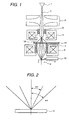
- FIG. 1 A schematic view of SEM equipped with a plate-like annular aperture body is shown as FIG. 1.
- An electron beam 2 has been taken out from an electron gun 1 and accelerated using an acceleration lens 3, is focused on a sample 8 by a focusing lens 4 and an objective lens 6.
- the focused beam is then scanned on the sample by a deflector 7, and the secondary electron 9 emitted from the sample is detected by a secondary-electron detector 10.
- An aperture body 11 for limiting the focused beam is located between deflector 7 and electron gun 1.
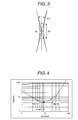
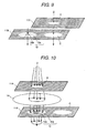
- Aperture body 11 has an annular aperture 12 as one of the apertures for limiting the passage of the electron beam, and the half-opening angle, ⁇ , of the electron beam focused on the sample stays within the band of specific values ⁇ a and ⁇ b ( ⁇ ⁇ a ) as shown in geometrically optical form in FIG. 2, wherein the passage of the electron is limited in the half-opening angle range from 0 degrees (optical axis) to ⁇ b .
- Aperture body 11 with annular aperture 12 and circular aperture 13 is shown in FIG. 5.
- the corresponding aperture body has the shape of a plate and is formed of tantalum (Ta) and molybdenum (Mo) materials.
- the aperture can have a heating means for cleaning dirt away therefrom.
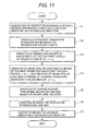
- FIG. 6 A comparative example of the calculation curve for the transfer function (also called the response function), ⁇ ( ⁇ D), that is used as a criterion for evaluating the SEM optical systems whose ⁇ values are 0 and 0.6, is shown in FIG. 6 to check the annulation effect of the aperture body.
- ⁇ ( ⁇ D) plotted along the vertical axis denotes changes in image contrast level.
- ⁇ in ⁇ D plotted along the horizontal axis denotes changes in wave number (spatial frequency)
- D denotes ⁇ / ⁇
- ⁇ D is a parameterized, dimensionless representation of " ⁇ ".
- ⁇ in ⁇ / ⁇ denotes ⁇ a .
- FIG. 6 (b) is an enlarged diagram of the ⁇ D data region from 1.2 to 2.0 in FIG. 6 (a).
- Parameters B, C, and D in calculation parameters B/D, C/D, and b/D denote spherical aberration, chromatic aberration, and the size of the electron gun virtual light source, respectively, and these parameters are defined using the following expressions:
- B (1/4)Cs ⁇ a 3
- R 0.1 can be improved at much the same ratio as that shown above.
- the electron gun used in the embodiment set forth above is of the Schottky
- a heating type tungsten [W] hairpin
- an electric field emission type is likewise available as an electron gun suitable for an electron microscope (the electric field emission type is further divided into two subtypes: cold and hot).
- the characteristics of these electron guns namely, luminance, the size, ⁇ , of a virtual light source, an energy spread, ⁇ E, and a beam current noise level
- TABLE 2 the characteristics of these electron guns.
- electron guns small in ⁇ and ⁇ E namely, the electric field emission type and Schottky type of electron guns are particularly excellent and this has also been confirmed experimentally.
- the ⁇ ( ⁇ D) curves in FIG. 6 are described in further detail below.
- image resolution, R 0.1 image resolution
- focal depth increases as ⁇ becomes closer to 1, since contrast deteriorates more significantly, a contradictory relationship exists between focal depth and contrast.
- the transmission ratio of electron wave intensity against an annular aperture whose annulation level is ⁇ can be expressed as (1 - ⁇ 2 ) from the aperture area ratio, and to obtain the same transmitted electron wave intensity as that achievable in the case of a circular aperture whose ⁇ is 1, the intensity of the electron wave radiated through the annular aperture must be increased to 1/(1 - ⁇ 2 ) times. This increases contrast by 1/(1 - ⁇ 2 ) times with respect to all frequency components, thus leading to the improvement of image quality. This improvement effect has also been experimentally confirmed.
- an aperture body having both a circular aperture and an annular aperture should be adopted.
- a movement feature not shown in the present embodiment is provided so that the above apertures are positioned on the passage route of the electron beam.
- aperture body 11 having a circular aperture 13 adjacent to the annular aperture 12 shown in FIG. 5 is formed to enable the selection of either according to the particular observation requirements.
- the selection of annular aperture 12 or circular aperture 13 is performed in the following sequence:
- the position of the aperture body is adjusted beforehand within a plane parallel to the aperture body surface so that the centers of annular aperture 12 and circular aperture 13 almost align with the optical axis.
- the beam position correction data and scan image rotational correction data to be applied to the deflector are registered along with the above-mentioned amounts of position adjustment.
- the appropriate data is retrieved from registered data so as to enable either aperture to be selected according to the particular requirements, and position setting of the apertures in the aperture body, the correction of the beam position, and the correction of scan image rotational errors are conducted.
- automatic multi-point observation based on the appropriate beam conditions can be implemented by adopting the configuration that permits the creation of a recipe which sets the annular aperture or the circular aperture, depending on the particular situation of the observation point.
- the apparatus has a control unit and a display unit, and the control unit is further equipped with a storage medium which can contain the data required for such aperture selection as mentioned above, and for automatic selection of another optical apparatus, with the two selection functions being performed in accordance with the data stored within the corresponding storage medium.
- Aperture body 11 in the embodiment described above is of a single-piece configuration.
- An embodiment using an aperture body of a two-piece configuration is described below using FIGS. 8 and 9.
- Aperture body 11 in this embodiment consists of two pieces: a circular aperture body 11A (a first plate-like body), which is located at the electron source side and has a circular aperture A, and a shielding disc/large-size circular aperture body 11B (a second plate-like body), which is located at the sample side and has a shielding disc 12b and a large circular aperture C adjacent thereto.
- Both aperture bodies are further provided with a movement feature that enables the corresponding aperture body to be independently moved along a plane parallel to that of the other aperture body, that is to say, a plane vertical to the optical axis, and thus the corresponding disc and aperture to be positioned on the orbit of the electron beam.
- FIGS. 8 and 9 show embodiments in which the circular aperture body 11A and the shielding disc/large-size circular aperture body 11B are combined to form an annular aperture and a circular aperture, respectively.
- An annular aperture body can be effectively created by moving it so that the centers of its circular aperture A and shielding disc/large-size circular aperture B overlap on the optical axis of objective lens 6.
- a circular aperture equivalent to the above-mentioned circular aperture A can be essentially created by moving the corresponding aperture body so that the centers of its circular aperture A and shielding disc/large-size circular aperture C overlap on the optical axis of objective lens 6.
- the creation of the annular aperture body consists of three steps: step 1, in which the center of circular aperture A is located on the optical axis of the objective lens; step 2, in which two-dimensional scanning of electron beam 2 by use of an aligner 5 is conducted on the circular aperture A of circular aperture body 11A (see FIG. 1), then either the rate of passage of the secondary electron emitted from sample 8, or the amount of current absorbed by circular aperture body 11A, at that time, is converted into a luminance signal, and scan-image G is created from this signal, and; step 3, in which, while the image of circular aperture A in scan-image G is being monitored, shielding disc 12b is located in the center of that image.
- the focusing point for the electron beam 2 scanned on circular aperture A in step 2 does not always need to be matched to the z-position of circular aperture A, it is desirable that the focusing point be matched to the z-position, because a sharper image of circular aperture A can be obtained in step 3 and because axial matching accuracy between circular aperture A and shielding disc 12b improves.
- the size (radius) ratio between circular aperture A, shielding disc 12b, and large circular aperture C, that is to be used for calculating the annulation level, ⁇ does not need to be adjusted.
- the annulation level, ⁇ is equal to r b /r a .
- the radius, r 11a of the aperture outer surface which forms shielding disc 12b is sufficiently great in comparison to r a .
- FIG. 10 an embodiment using the aperture body 11 which requires the adjustment of the size (radius) of its aperture during the calculation of the annulation level, ⁇ , is shown in FIG. 10.
- this aperture body 11 is a two-piece body consisting of circular aperture body 11A and shielding disc/large circular aperture body 11B, lens 4 exists between both aperture bodies.
- the annulation level, ⁇ can be represented using the expression shown below.
- the radius, r 12a , of the aperture outer surface 12a which retains shielding disc 12b is sufficiently great in comparison to r a,11B .
- circular aperture body 11A with circular aperture A is located at the electron source side and shielding disc/large circular aperture body 11B with both shielding disc 12b and large circular aperture C adjacent thereto is located at the sample side, similar effects can be obtained, even if the arrangement of these aperture bodies is opposite.
- FIG. 1 shows an example of SEM in which secondary electron 9 emitted from the surface of the sample during electron beam irradiation is used to create luminance signal information on an electron microscope image. If the electron acceleration voltage is increased above about 100 kV and the thickness of the sample is reduced to the range from several tens to several hundred nanometers, the electron beam that has transmitted the corresponding sample can also be used.
- a microscope image based on a secondary electron provides surface information relating mainly to the sample, whereas a microscope image based on a transmitted electron beam provides internal information on the sample.
- the apparatus according to this embodiment uses a secondary electron to create an image of a sample
- the embodiment is not limited to such an application and can likewise be applied to an apparatus which uses a reflected electron to create an image of a sample.
- FIG. 11 The flow of processing in which both images are to be used to create and display a new microscope image F is shown as FIG. 11.
- S1 the electron microscope images D and E obtained via a circular aperture and an annular aperture are photographed and then recorded as digital information.
- the intensity (more exactly, the irradiation angle current density) of the electron beam radiated from the electron gun is doubled to ensure that the electron microscope image E at the annular aperture is photographed with twice the intensity of the beam after it has passed through the aperture.
- S2 Fourier transform images based on microscope images D and E are created as D F and E F , respectively.
- image D FBL by low-pass filtering of Fourier transform image D FB through the ⁇ c region at a spatial frequency, ⁇ is created, whereas image E FBL by low-pass filtering of Fourier transform image E FB through the ⁇ c is created.
- the summation-based image F has the features that this image, is one to two times improved over image C in terms of the contrast level of the high-frequency components in the ⁇ c region and that focal depth is improved by several tens of percent. In addition, image resolution is improved by several percent.
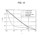
- ⁇ ( ⁇ D) Three types of curves ... namely, ⁇ c ( ⁇ D) and ⁇ A ( ⁇ D) curves of the electron microscope images obtained when a circular aperture and an annular aperture were used, and a ⁇ c+A ( ⁇ D) curve of the electron microscope image corresponding to the summation-based image F created by low-pass filtering and high-pass filtering, are shown in FIG. 12 for comparison.
- both the focal depth and resolution of a charged-particle microscope which scans the surface of a sample can be improved at the same time.
Landscapes
- Chemical & Material Sciences (AREA)
- Analytical Chemistry (AREA)
- Analysing Materials By The Use Of Radiation (AREA)
- Electron Sources, Ion Sources (AREA)
Abstract
Description
| (C/D, b/D) | β = 0 | β = 0.6 | Improvement ratio [%] | |||
| D/R0.1 | Δzα/D | D/R0.1 | Δzα/D | D/R0.1 | Δzα/D | |
| (0, 0) | 1.61 | 1.03 | 1.71 | 1.61 | 6 | 56 |
| (0.4, 0) | 1.60 | 1.10 | 1.71 | 1.66 | 6 | 51 |
| (0.4, 0.1) | 1.53 | - | 1.65 | - | 7 | - |
| Heating type (W hairpin) | Electric field emission type | Shottky type | ||
| Cold | Hot | |||
| Luminance | 103 | 103 | 5 × 10³ | 5 × 10³ |
| ρ | 20 - 50µm | 3nm | 30nm | 15nm |
| ΔE[eV] | 1 - 2 | 0.2 - 0.3 | 0.8 - 1.8 | 0.3 - 0.7 |
| Beam current noise [%RMS] | < 0.5 | 4 - 6 | 5 - 10 | < 1 |
Claims (12)
- A scanning charged-particle microscope havingwherein said scanning charged-particle microscope is characterized in that a passage aperture (12) for limiting the passage of the charged-particle optical beam is located between the charged-particle source (1) and said scanning deflector (7) and in that a member (12b) for limiting the passage of the charged-particle optical beam (2) is provided at least in the center of said passage aperture (12).a charged-particle source (1),a lens (4) for focusing the charged-particle optical beam (2) emitted from said charged-particle source (1), anda scanning deflector (7) for scanning said charged-particle optical beam (2) in two-dimensional form on a sample,
- A scanning charged-particle microscope as set forth in claim 1 above, wherein the scanning charged-particle microscope is characterized in that the half-opening angle of said aperture (12) for said charged-particle optical beam (2) focused on a sample (8) by said focusing lens has a band with respect to specific values of αa and αb.
- A scanning charged-particle microscope as set forth in claim 1 above, wherein the scanning charged-particle microscope is characterized in that said passage aperture (12) is formed in a plate-like body (11), and in that said plate-like body (11) is formed movably with respect to said charged-particle optical beam (2).
- A scanning charged-particle microscope as set forth in claim 3 above, wherein the scanning charged-particle microscope is characterized in that said plate-like body (11) is provided with a circular aperture (13) in addition to said passage aperture (12).
- A scanning charged-particle microscope havingwherein said scanning charged-particle microscope is characterized in that it has a means by which said charged-particle optical beam (2) focused on said sample is radiated so that the half-opening angle of said aperture for the charged-particle optical beam will have a band with respect to specific values of αa and αb.a charged-particle source (1),a lens (4) for focusing the charged-particle optical beam (2) emitted from said charged-particle source (1), anda scanning deflector (7) for scanning said charged-particle optical beam (2) in two-dimensional form on a sample,
- A scanning charged-particle microscope as set forth in claim 5 above, wherein the scanning charged-particle microscope is characterized in that a plate-like aperture body (11) in which an annular aperture (12) is formed is provided between said charged-particle source (1) and said scanning deflector (7).
- A scanning charged-particle microscope as set forth in claim 6 above, wherein the scanning charged-particle microscope is characterized in that in addition to said annular aperture (12), a circular aperture (13) is provided in said plate-like aperture body, and in that there is provided a movement feature for positioning said annular aperture (12) and said circular aperture (13) on the orbit of said charged-particle optical beam.
- A scanning charged-particle microscope havingwherein said scanning charged-particle microscope is characterized in that an aperture for limiting the passage of said charged-particle optical beam is formed in two different places on the orbit thereof, and in that one of said two apertures is an annular aperture (12) and the other is a circular aperture (A).a charged-particle source (1),a lens (4) for focusing the charged-particle optical beam (2) emitted from said charged-particle source (1), anda scanning deflector (7) for scanning said charged-particle optical beam (2) in two-dimensional form on a sample,
- A scanning charged-particle microscope as set forth in claim 8 above, wherein the scanning charged-particle microscope is characterized in that said annular aperture (12) is formed in a plate-like body (11), in that said plate-like body (11) is also provided with a circular aperture (13), and in that there is provided a movement feature for positioning the annular aperture (12) and the circular aperture (13) on the orbit of said charged-particle optical beam.
- A scanning charged-particle microscope as set forth in claim 8 above, wherein the scanning charged-particle microscope is characterized in that said circular aperture (A) is formed in a plate-like body (11A), in that said plate-like body (11A) is also provided with a charged-particle optical beam cutoff portion, and in that there is provided a movement feature for positioning said charged-particle optical beam cutoff portion and said circular aperture on the orbit of said charged-particle optical beam.
- A scanning charged-particle microscope as set forth in claim 8 above, wherein the scanning charged-particle microscope is characterized in that said circular aperture (A) and said annular aperture (12) are formed in a first plate-like body (11A) and a second plate-like body (11B), respectively, in that said first plate-like body (11A) is provided with a charged-particle optical beam cutoff portion in addition to the circular aperture (A) and said second plate-like body (11B) is provided with a circular aperture (C) in addition to the annular aperture (12), and in that both the first plate-like body (11A) and the second plate-like body (11B) are provided with a movement feature.
- A samples image forming method using a scanning charged-particle microscope havingwherein said samples image forming method is characterized in that the image of a sample that has been acquired with an annular aperture (12) positioned on the orbit of the charged-particle optical beam and the image of a sample that has been acquired with a circular aperture (C) positioned on the orbit of the charged-particle optical beam are combined to form a new samples image.a charged-particle source (1),a lens (4) for focusing the charged-particle optical beam (2) emitted from said charged-particle source (1), anda scanning deflector (7) for scanning said charged-particle optical beam (2) in two-dimensional form on a sample,
Applications Claiming Priority (2)
| Application Number | Priority Date | Filing Date | Title |
|---|---|---|---|
| JP2000316843 | 2000-10-12 | ||
| JP2000316843A JP3987276B2 (en) | 2000-10-12 | 2000-10-12 | Sample image forming method |
Publications (3)
| Publication Number | Publication Date |
|---|---|
| EP1197985A2 true EP1197985A2 (en) | 2002-04-17 |
| EP1197985A3 EP1197985A3 (en) | 2006-07-26 |
| EP1197985B1 EP1197985B1 (en) | 2009-08-12 |
Family
ID=18795732
Family Applications (1)
| Application Number | Title | Priority Date | Filing Date |
|---|---|---|---|
| EP01120621A Expired - Lifetime EP1197985B1 (en) | 2000-10-12 | 2001-08-29 | Scanning charged-particle microscope |
Country Status (4)
| Country | Link |
|---|---|
| US (1) | US7186975B2 (en) |
| EP (1) | EP1197985B1 (en) |
| JP (1) | JP3987276B2 (en) |
| DE (1) | DE60139535D1 (en) |
Cited By (2)
| Publication number | Priority date | Publication date | Assignee | Title |
|---|---|---|---|---|
| EP1577926A1 (en) * | 2004-03-19 | 2005-09-21 | ICT, Integrated Circuit Testing Gesellschaft für Halbleiterprüftechnik Mbh | High current density particle beam system |
| EP2511938A4 (en) * | 2009-12-07 | 2014-03-12 | Hitachi High Tech Corp | ELECTRONIC TRANSMISSION MICROSCOPE AND METHOD OF OBSERVING TEST SAMPLES |
Families Citing this family (20)
| Publication number | Priority date | Publication date | Assignee | Title |
|---|---|---|---|---|
| DE10301579A1 (en) * | 2003-01-16 | 2004-07-29 | Leo Elektronenmikroskopie Gmbh | Electron beam device and detector arrangement |
| US7173259B2 (en) * | 2004-06-09 | 2007-02-06 | Taiwan Semiconductor Manufacturing Co., Ltd. | Automatically aligning objective aperture for a scanning electron microscope |
| JP4445893B2 (en) * | 2005-04-06 | 2010-04-07 | 株式会社日立ハイテクノロジーズ | Scanning electron microscope |
| JP4708854B2 (en) | 2005-05-13 | 2011-06-22 | 株式会社日立ハイテクノロジーズ | Charged particle beam equipment |
| US8026491B2 (en) * | 2006-03-08 | 2011-09-27 | Hitachi High-Technologies Corporation | Charged particle beam apparatus and method for charged particle beam adjustment |
| JP2009531855A (en) * | 2006-03-27 | 2009-09-03 | マルチビーム システムズ インコーポレイテッド | Optical system for generating high current density patterned charged particle beams |
| US7947964B2 (en) * | 2006-11-21 | 2011-05-24 | Hitachi High-Technologies Corporation | Charged particle beam orbit corrector and charged particle beam apparatus |
| JP5438937B2 (en) * | 2008-09-05 | 2014-03-12 | 株式会社日立ハイテクノロジーズ | Charged particle beam equipment |
| JP5277250B2 (en) * | 2008-09-25 | 2013-08-28 | 株式会社日立ハイテクノロジーズ | Charged particle beam application apparatus and geometric aberration measuring method thereof |
| JP5677081B2 (en) | 2010-12-28 | 2015-02-25 | 株式会社日立ハイテクノロジーズ | Charged particle beam equipment |
| JP5581248B2 (en) * | 2011-03-08 | 2014-08-27 | 株式会社日立ハイテクノロジーズ | Scanning electron microscope |
| EP2704177B1 (en) * | 2012-09-04 | 2014-11-26 | Fei Company | Method of investigating and correcting aberrations in a charged-particle lens system |
| JP6470654B2 (en) * | 2015-07-24 | 2019-02-13 | 株式会社日立ハイテクノロジーズ | Charged particle beam equipment |
| US10460905B2 (en) * | 2015-09-23 | 2019-10-29 | Kla-Tencor Corporation | Backscattered electrons (BSE) imaging using multi-beam tools |
| CN108885961B (en) | 2016-03-29 | 2020-05-01 | 株式会社日立高新技术 | Electron microscope |
| JP6900026B2 (en) * | 2017-03-27 | 2021-07-07 | 株式会社日立ハイテクサイエンス | Charged particle beam device |
| JP6913344B2 (en) * | 2017-03-27 | 2021-08-04 | 株式会社日立ハイテクサイエンス | Charged particle beam device |
| JP2020181629A (en) | 2017-07-27 | 2020-11-05 | 株式会社日立ハイテク | Electron beam observation device, electron beam observation system, and control method for electron beam observation device |
| EP3550585B1 (en) * | 2018-04-05 | 2021-06-23 | FEI Company | Studying dynamic specimens in a transmission charged particle microscope |
| WO2020157809A1 (en) | 2019-01-28 | 2020-08-06 | 株式会社日立ハイテク | Electron beam application device |
Family Cites Families (17)
| Publication number | Priority date | Publication date | Assignee | Title |
|---|---|---|---|---|
| US3714422A (en) * | 1970-04-06 | 1973-01-30 | Hitachi Ltd | Scanning stereoscopic electron microscope |
| DE2043749C3 (en) * | 1970-08-31 | 1975-08-21 | Max-Planck-Gesellschaft Zur Foerderung Der Wissenschaften E.V., 3400 Goettingen | Scanning corpuscular beam microscope |
| US3996468A (en) * | 1972-01-28 | 1976-12-07 | Nasa | Electron microscope aperture system |
| GB1416043A (en) | 1972-01-28 | 1975-12-03 | Nasa | Electron microscope aperture system |
| JPS60105149A (en) * | 1983-11-11 | 1985-06-10 | Jeol Ltd | Electron-ray device |
| US5866905A (en) * | 1991-05-15 | 1999-02-02 | Hitachi, Ltd. | Electron microscope |
| JPH09167591A (en) * | 1995-12-15 | 1997-06-24 | Hitachi Ltd | Scanning transmission electron microscope |
| JPH0594798A (en) | 1991-05-21 | 1993-04-16 | Jeol Ltd | Electron optical observation device such as electron microscope with switchable depth of focus |
| JPH05258700A (en) | 1992-03-13 | 1993-10-08 | Jeol Ltd | Scanning image observing method and scanning electron microscope |
| JP3416270B2 (en) | 1994-07-01 | 2003-06-16 | 三洋電機株式会社 | Micro spot forming method and apparatus for implementing the method |
| JPH08138600A (en) | 1994-11-04 | 1996-05-31 | Shimadzu Corp | Charged particle optics |
| DE69638126D1 (en) * | 1995-10-19 | 2010-04-01 | Hitachi Ltd | scanning Electron Microscope |
| US5821542A (en) * | 1996-06-26 | 1998-10-13 | International Business Machines Corporation | Particle beam imaging system having hollow beam illumination |
| JPH11186150A (en) | 1997-12-16 | 1999-07-09 | Nikon Corp | Charged particle beam exposure apparatus, mask alignment method therefor, and apparatus calibration method |
| JP2000012454A (en) | 1998-06-25 | 2000-01-14 | Nikon Corp | Electron beam exposure equipment |
| JPH11297610A (en) * | 1998-04-08 | 1999-10-29 | Nikon Corp | Charged particle beam exposure system |
| JP2000299081A (en) * | 1999-04-14 | 2000-10-24 | Jeol Ltd | Transmission electron microscope |
-
2000
- 2000-10-12 JP JP2000316843A patent/JP3987276B2/en not_active Expired - Lifetime
-
2001
- 2001-08-29 EP EP01120621A patent/EP1197985B1/en not_active Expired - Lifetime
- 2001-08-29 DE DE60139535T patent/DE60139535D1/en not_active Expired - Lifetime
- 2001-08-30 US US09/943,262 patent/US7186975B2/en not_active Expired - Lifetime
Cited By (4)
| Publication number | Priority date | Publication date | Assignee | Title |
|---|---|---|---|---|
| EP1577926A1 (en) * | 2004-03-19 | 2005-09-21 | ICT, Integrated Circuit Testing Gesellschaft für Halbleiterprüftechnik Mbh | High current density particle beam system |
| WO2005096343A1 (en) * | 2004-03-19 | 2005-10-13 | Ict, Integrated Circuit Testing Gesellschaft Für Halbleiterprüftechnik Mbh | High current density particle beam system |
| US7663102B2 (en) | 2004-03-19 | 2010-02-16 | ICT Integrated Circuit Testing Gesellschaft für Halbleiterprüftechnik mbH | High current density particle beam system |
| EP2511938A4 (en) * | 2009-12-07 | 2014-03-12 | Hitachi High Tech Corp | ELECTRONIC TRANSMISSION MICROSCOPE AND METHOD OF OBSERVING TEST SAMPLES |
Also Published As
| Publication number | Publication date |
|---|---|
| JP3987276B2 (en) | 2007-10-03 |
| EP1197985A3 (en) | 2006-07-26 |
| US7186975B2 (en) | 2007-03-06 |
| EP1197985B1 (en) | 2009-08-12 |
| US20020079448A1 (en) | 2002-06-27 |
| DE60139535D1 (en) | 2009-09-24 |
| JP2002124205A (en) | 2002-04-26 |
Similar Documents
| Publication | Publication Date | Title |
|---|---|---|
| US7186975B2 (en) | Scanning charged-particle microscope | |
| KR102480232B1 (en) | Apparatus of Plural Charged-Particle Beams | |
| US7223983B2 (en) | Charged particle beam column | |
| US8426811B2 (en) | Electron microscope | |
| US8405025B2 (en) | Scanning electron microscope and method for detecting an image using the same | |
| EP2091062A1 (en) | TEM with aberration corrector and phase plate | |
| US20080265161A1 (en) | Electron Microscope And Electron Beam Inspection System | |
| US8642959B2 (en) | Method and system of performing three-dimensional imaging using an electron microscope | |
| JPH11148905A (en) | Electron beam inspection method and apparatus | |
| EP2378537B1 (en) | Method of operating a charged particle beam device | |
| JP4553889B2 (en) | Determination method of aberration coefficient in aberration function of particle optical lens | |
| JP2005032732A (en) | Scanning electron microscope | |
| JP2002184336A (en) | Charged particle beam microscope device, charged particle beam application device, charged particle beam microscopy method, charged particle beam inspection method, and electron microscope device | |
| TW202501532A (en) | Charged particle beam device | |
| Joy | The aberration-corrected SEM | |
| JP2007207764A (en) | Scanning charged particle microscope | |
| CN114300325A (en) | Charged particle beam device and adjustment method | |
| JP5389124B2 (en) | Scanning charged particle beam equipment | |
| WO2026006804A1 (en) | Scanning transmission electron microscope resolution and contrast improvement | |
| JP2019169362A (en) | Electron beam device | |
| JPS6029187B2 (en) | electronic microscope | |
| JP4475613B2 (en) | Emission electron microscope | |
| JPH0234142B2 (en) | ||
| JP2004199884A (en) | Electron diffraction device | |
| EP1585165A2 (en) | Electron microscope |
Legal Events
| Date | Code | Title | Description |
|---|---|---|---|
| PUAI | Public reference made under article 153(3) epc to a published international application that has entered the european phase |
Free format text: ORIGINAL CODE: 0009012 |
|
| AK | Designated contracting states |
Kind code of ref document: A2 Designated state(s): AT BE CH CY DE DK ES FI FR GB GR IE IT LI LU MC NL PT SE TR |
|
| AX | Request for extension of the european patent |
Free format text: AL;LT;LV;MK;RO;SI |
|
| PUAL | Search report despatched |
Free format text: ORIGINAL CODE: 0009013 |
|
| AK | Designated contracting states |
Kind code of ref document: A3 Designated state(s): AT BE CH CY DE DK ES FI FR GB GR IE IT LI LU MC NL PT SE TR |
|
| AX | Request for extension of the european patent |
Extension state: AL LT LV MK RO SI |
|
| 17P | Request for examination filed |
Effective date: 20070126 |
|
| AKX | Designation fees paid |
Designated state(s): DE FR GB NL |
|
| 17Q | First examination report despatched |
Effective date: 20070316 |
|
| GRAP | Despatch of communication of intention to grant a patent |
Free format text: ORIGINAL CODE: EPIDOSNIGR1 |
|
| GRAS | Grant fee paid |
Free format text: ORIGINAL CODE: EPIDOSNIGR3 |
|
| GRAA | (expected) grant |
Free format text: ORIGINAL CODE: 0009210 |
|
| RAP1 | Party data changed (applicant data changed or rights of an application transferred) |
Owner name: HITACHI, LTD. |
|
| AK | Designated contracting states |
Kind code of ref document: B1 Designated state(s): DE FR GB NL |
|
| REG | Reference to a national code |
Ref country code: GB Ref legal event code: FG4D |
|
| REF | Corresponds to: |
Ref document number: 60139535 Country of ref document: DE Date of ref document: 20090924 Kind code of ref document: P |
|
| PLBE | No opposition filed within time limit |
Free format text: ORIGINAL CODE: 0009261 |
|
| STAA | Information on the status of an ep patent application or granted ep patent |
Free format text: STATUS: NO OPPOSITION FILED WITHIN TIME LIMIT |
|
| 26N | No opposition filed |
Effective date: 20100517 |
|
| GBPC | Gb: european patent ceased through non-payment of renewal fee |
Effective date: 20091112 |
|
| PG25 | Lapsed in a contracting state [announced via postgrant information from national office to epo] |
Ref country code: GB Free format text: LAPSE BECAUSE OF NON-PAYMENT OF DUE FEES Effective date: 20091112 |
|
| REG | Reference to a national code |
Ref country code: FR Ref legal event code: ST Effective date: 20110502 |
|
| PG25 | Lapsed in a contracting state [announced via postgrant information from national office to epo] |
Ref country code: FR Free format text: LAPSE BECAUSE OF NON-PAYMENT OF DUE FEES Effective date: 20091012 |
|
| PGFP | Annual fee paid to national office [announced via postgrant information from national office to epo] |
Ref country code: NL Payment date: 20140710 Year of fee payment: 14 |
|
| REG | Reference to a national code |
Ref country code: NL Ref legal event code: MM Effective date: 20150901 |
|
| PG25 | Lapsed in a contracting state [announced via postgrant information from national office to epo] |
Ref country code: NL Free format text: LAPSE BECAUSE OF NON-PAYMENT OF DUE FEES Effective date: 20150901 |
|
| PGFP | Annual fee paid to national office [announced via postgrant information from national office to epo] |
Ref country code: DE Payment date: 20200819 Year of fee payment: 20 |
|
| REG | Reference to a national code |
Ref country code: DE Ref legal event code: R071 Ref document number: 60139535 Country of ref document: DE |