EP1195913A1 - Amplifier arrangement - Google Patents
Amplifier arrangement Download PDFInfo
- Publication number
- EP1195913A1 EP1195913A1 EP00402752A EP00402752A EP1195913A1 EP 1195913 A1 EP1195913 A1 EP 1195913A1 EP 00402752 A EP00402752 A EP 00402752A EP 00402752 A EP00402752 A EP 00402752A EP 1195913 A1 EP1195913 A1 EP 1195913A1
- Authority
- EP
- European Patent Office
- Prior art keywords
- signal
- hybrid
- function
- receive
- transmit
- Prior art date
- Legal status (The legal status is an assumption and is not a legal conclusion. Google has not performed a legal analysis and makes no representation as to the accuracy of the status listed.)
- Granted
Links
- 230000009131 signaling function Effects 0.000 claims abstract description 19
- 230000006870 function Effects 0.000 claims description 30
- 230000003044 adaptive effect Effects 0.000 description 2
- 230000007246 mechanism Effects 0.000 description 2
- YEJRWHAVMIAJKC-UHFFFAOYSA-N 4-Butyrolactone Chemical compound O=C1CCCO1 YEJRWHAVMIAJKC-UHFFFAOYSA-N 0.000 description 1
- 102400001284 Vessel dilator Human genes 0.000 description 1
- 101800001899 Vessel dilator Proteins 0.000 description 1
- 230000008859 change Effects 0.000 description 1
- 230000001419 dependent effect Effects 0.000 description 1
- 230000010354 integration Effects 0.000 description 1
- 230000004048 modification Effects 0.000 description 1
- 238000012986 modification Methods 0.000 description 1
- RGCLLPNLLBQHPF-HJWRWDBZSA-N phosphamidon Chemical compound CCN(CC)C(=O)C(\Cl)=C(/C)OP(=O)(OC)OC RGCLLPNLLBQHPF-HJWRWDBZSA-N 0.000 description 1
- 230000009467 reduction Effects 0.000 description 1
Images


Classifications
-
- H—ELECTRICITY
- H04—ELECTRIC COMMUNICATION TECHNIQUE
- H04B—TRANSMISSION
- H04B1/00—Details of transmission systems, not covered by a single one of groups H04B3/00 - H04B13/00; Details of transmission systems not characterised by the medium used for transmission
- H04B1/38—Transceivers, i.e. devices in which transmitter and receiver form a structural unit and in which at least one part is used for functions of transmitting and receiving
- H04B1/40—Circuits
- H04B1/54—Circuits using the same frequency for two directions of communication
- H04B1/58—Hybrid arrangements, i.e. arrangements for transition from single-path two-direction transmission to single-direction transmission on each of two paths or vice versa
- H04B1/583—Hybrid arrangements, i.e. arrangements for transition from single-path two-direction transmission to single-direction transmission on each of two paths or vice versa using a bridge network
- H04B1/585—Hybrid arrangements, i.e. arrangements for transition from single-path two-direction transmission to single-direction transmission on each of two paths or vice versa using a bridge network with automatic balancing
Definitions
- the present invention relates to an amplifier arrangement for broadband signal.
- receivers for broadband communication systems such as for asynchronous or asymmetric data(digital) subscriber loop (ADSL), or for high velocity data subscriber loop (VDSL), etc.
- Some of the known receivers provide an adaptive mechanism for reducing echo, such mechanism being for example a tuneable balance impedance on the balance of a classical hybrid as disclosed in IEEE JOURNAL ON SELECTED AREAS IN COMMUNICATIONS, Vol. 9 No. 6, August 1991, WALTER Y.CHEN, JAMES L.DIXON, DAVID L.WARING, "High Bit Rate Digital Subscriber Line Echo Cancellation".
- Said transformers are expensive and inflexible.
- Another example is a straight-forward wheatstone-bridge hybrid where one of the impedances can be tuned, as disclosed in ISSCC99/Sessions 14/paper tp14.4, MICHAEL MOYAL, MARTIN GROEPL, THOMAS BLON, "A 25 kft 768kb/s CMOS Transceiver for Multiple Bit-Rate DSL".
- the amplifier arrangement of the invention is an arrangement enabling an efficient reduction of the noise without transformers.
- Other advantages of amplifier arrangement of the invention will be disclosed when describing a preferred embodiment of the arrangement of the invention.
- the amplifier arrangement for transmitting and receiving a broadband signal of the invention comprises :
- the tuneable gain means is adapted for converting the transmit hybrid signal into a gained transmit hybrid signal corresponding substantially to the reverse of or substantially equal to a portion of the receive hybrid signal corresponding to or function of the transmitted signal passing through the receive hybrid means, while the signal treatment means is adapted to add or subtract the gained transmit hybrid signal to and/or from the receive hybrid signal, whereby said treatment is adapted for generating a signal which is substantially independent of the transmitted signal or a function thereof.
- the resistive transmit hybrid means is adapted to tune said gain so that the gained transmit hybrid signal is substantially reverse to the portion of the transmitted signal passing through the receive hybrid means.
- the signal treatment means is advantageously adapted for adding the signal passed by the receive hybrid means and the gained transmit hybrid signal of said transmit hybrid means together.
- the signal treatment means is then a differential inverter amplifier.
- the resistive receive hybrid means comprises four resistors adapted for receiving a first signal function and a second signal function, each signal function comprising a linear combination of a receive signal and a transmit signal, said resistors being adapted for transferring a receive hybrid signal which is function of the difference between the first signal function and the second signal function.
- the resistive transmit hybrid means comprises four tuneable resistors adapted for receiving a first signal function and a second signal function, each signal function comprising a linear combination of a receive signal and a transmit signal, said resistors being adapted for transferring a transmit hybrid signal function of the difference between a linear combination of the first signal and a linear combination of the second function, whereby one of said linear combinations or said combinations are adapted so that said difference in not function of the receive signal.
- the amplifier arrangement of the invention comprises advantageously an automatic gain control means and/or a line driver means for synthesising at least two combinations comprising each a linear combination of a receive signal and a transmit signal.
- the invention relates also to the use of an amplifier arrangement of the invention in a broadband communication system, such as ASDL, VSDL, etc.
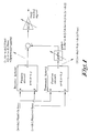
- Figure 1 is a schematic view of a preferred amplifier arrangement of the invention.
- Said amplifier arrangement is adapted for treating two linearly independent combinations of two signals (Vrec or V received or useful signal, Vtmt or V transmitted or noise-spurious signal).
- the amplifier arrangement comprises :
- the gained hybrid transmit signal is reversed (mutiplied by -1) and the reversed gained transmit hybrid signal and the receive hybrid signal are added together using an automatic gain control (AGC).
- AGC automatic gain control
- the signal is only a function of Vrec and can possibly be equal to Vrec.
- Figure 2 is an electrical schematic view of an amplifier arrangement of the invention.
- Vrec and Vtmt are signals present over the nodes 2-2' of the net.
- Vtmt is generated by the transceiver depicted at figure 2
- Vrec is generated by the transceiver at the other side of the line.
- the amplifier comprises a first receive hybrid comprising the resistors R and (1+ ⁇ ).R and a second transmit hybrid comprising tuneable resistors R1.
- the hybrids are mounted in parallel.
- the output signal of the receiver (Vout) is equal to: (2 ⁇ / (1+ ⁇ )). (Rg/R). [Vrec + [((Zin - Rh)/(Zin + Rh)) + (k.(1+ ⁇ ) R/R1)].Vtmt]
- R and R1 are such that R>>Rh and R1>>Rh.
- the echo cancelling is realised by a hybrid structure of four resistors related to R1 that is adapted to inject a signal at the inputs of the differential receiver DF, that is proportional to the transmitted signal, in order to cancel the echo at the output of the receiver.
- the hybrid structure of resistors based on R1 passes only transmitted signal or a function thereof in all situations.
- each tuneable resistor R1 By switching as many resistors as needed to the summation node, the value can be tuned. If a resistor R1 is not used, it is switched to the ground. As the opamp input is virtually at ground and as R1 is a relatively high resistor, the circuit does not suffer from switch distortion. Possible noise due to R1 is not important, as in practice R1 is much higher than R, whereby the parallel equivalent noise source due to R1 is much lower.
- the circuit combines echo cancellation with automatic gain control (AGC).
- AGC automatic gain control
- the resistor R1 of the transmit hybrid can be replaced by complex Z1, so as to render possible at least an attenuation, preferably the cancellation of the quadrature part of the echo. It is possible also to add other signal(s) to the amplifier arrangement, for example RFI cancellation signals.
- the amplifier of figure 2 is suitable for lowering the echo for VDSL over normal telephone loops. This lowers then the requirements and therefore dissipation, cost, complexity, etc. of all other components in transmit and receive path (such as DAC, ADC, filter, PGA, line driver, etc. ) with 5-10 dB.
- the amplifier of figure 2 enables to increase the performance of a existing modem.
Landscapes
- Engineering & Computer Science (AREA)
- Computer Networks & Wireless Communication (AREA)
- Signal Processing (AREA)
- Amplifiers (AREA)
- Semiconductor Lasers (AREA)
- Variable-Direction Aerials And Aerial Arrays (AREA)
Abstract
- a resistive receive hybrid means adapted to pass a combination of a received signal and a transmitted signal,
- a resistive transmit hybrid means adapted to pass substantially only the transmitted signal,
- a tuneable gain means adapted for converting the transmit hybrid signal into a signal corresponding substantially to the reverse of the portion of the receive hybrid signal function of the transmitted signal passing through the receive hybrid means,
- signal treatment means adapted to add or subtract the gained signal to and/or from the receive hybrid signal, whereby said treatment is adapted for generating a signal which is substantially independent of the transmitted signal.
Description
- The present invention relates to an amplifier arrangement for broadband signal.
- It is known to use receivers for broadband communication systems, such as for asynchronous or asymmetric data(digital) subscriber loop (ADSL), or for high velocity data subscriber loop (VDSL), etc. Some of the known receivers provide an adaptive mechanism for reducing echo, such mechanism being for example a tuneable balance impedance on the balance of a classical hybrid as disclosed in IEEE JOURNAL ON SELECTED AREAS IN COMMUNICATIONS, Vol. 9 No. 6, August 1991, WALTER Y.CHEN, JAMES L.DIXON, DAVID L.WARING, "High Bit Rate Digital Subscriber Line Echo Cancellation". Said transformers are expensive and inflexible.
- Another example is a straight-forward wheatstone-bridge hybrid where one of the impedances can be tuned, as disclosed in ISSCC99/Sessions 14/paper tp14.4, MICHAEL MOYAL, MARTIN GROEPL, THOMAS BLON, "A 25 kft 768kb/s CMOS Transceiver for Multiple Bit-Rate DSL".
- In the current art adaptive echo-cancelling is never combined with active back termination (EP-A-0.901.221). This reduces the power efficiency.
- Moreover the "matching path" in the wheatstone-bridge implementation is noisy when high impedant or power consuming when low impedant.
- The amplifier arrangement of the invention is an arrangement enabling an efficient reduction of the noise without transformers. Other advantages of amplifier arrangement of the invention will be disclosed when describing a preferred embodiment of the arrangement of the invention.
- The amplifier arrangement for transmitting and receiving a broadband signal of the invention comprises :
- a resistive receive hybrid means adapted to pass a receive hybrid signal selected from the group consisting of combinations of a received signal and a transmitted signal, signals function of the received signal and of the transmitted signal, and combinations thereof,
- a resistive transmit hybrid means that is adapted to pass a transmit hybrid signal corresponding substantially only the transmitted signal or a portion thereof or a function thereof,
- a tuneable gain means adapted for converting the transmit hybrid signal into a gained transmit hybrid signal corresponding substantially to the reverse of or substantially equal to a portion of the receive hybrid signal corresponding to or function of the transmitted signal passing through the receive hybrid means, and/or for converting the receive hybrid signal into a gained received hybrid signal, the portion of which is function of the transmitted signal corresponding to the reverse of or being substantially equal to the transmit hybrid signal or to a function thereof,
- signal treatment means adapted to add or subtract the gained transmit hybrid signal to and/or from a signal selected from the group consisting of the receive hybrid signal, a gained receive hybrid signal and/or a function thereof, and/or to add or subtract the gained receive hybrid signal to and/or from a signal selected from the group consisting- of the transmit hybrid signal, a gained transmit hybrid signal and/or a function thereof, whereby said treatment is adapted for generating a signal which is substantially independent of the transmitted signal or a function thereof.
- Advantageously, the tuneable gain means is adapted for converting the transmit hybrid signal into a gained transmit hybrid signal corresponding substantially to the reverse of or substantially equal to a portion of the receive hybrid signal corresponding to or function of the transmitted signal passing through the receive hybrid means, while the signal treatment means is adapted to add or subtract the gained transmit hybrid signal to and/or from the receive hybrid signal, whereby said treatment is adapted for generating a signal which is substantially independent of the transmitted signal or a function thereof.
- Preferably, the resistive transmit hybrid means is adapted to tune said gain so that the gained transmit hybrid signal is substantially reverse to the portion of the transmitted signal passing through the receive hybrid means. In said case, the signal treatment means is advantageously adapted for adding the signal passed by the receive hybrid means and the gained transmit hybrid signal of said transmit hybrid means together. Preferably, the signal treatment means is then a differential inverter amplifier.
- According to a detail of an advantageous embodiment, the resistive receive hybrid means comprises four resistors adapted for receiving a first signal function and a second signal function, each signal function comprising a linear combination of a receive signal and a transmit signal, said resistors being adapted for transferring a receive hybrid signal which is function of the difference between the first signal function and the second signal function.
- According to still another detail of an advantageous embodiment, the resistive transmit hybrid means comprises four tuneable resistors adapted for receiving a first signal function and a second signal function, each signal function comprising a linear combination of a receive signal and a transmit signal, said resistors being adapted for transferring a transmit hybrid signal function of the difference between a linear combination of the first signal and a linear combination of the second function, whereby one of said linear combinations or said combinations are adapted so that said difference in not function of the receive signal.
- The amplifier arrangement of the invention comprises advantageously an automatic gain control means and/or a line driver means for synthesising at least two combinations comprising each a linear combination of a receive signal and a transmit signal.
- The invention relates also to the use of an amplifier arrangement of the invention in a broadband communication system, such as ASDL, VSDL, etc.
- Details and characteristics of the invention will appear from the following description in which reference is made to the attached drawings for the description of a preferred embodiment of the amplifier arrangement of the invention.
- In said drawings,
- figure 1 is a schematic view of a preferred embodiment of the invention ;
- figure 2 is a view showing an electrical circuit for carrying the functions shown in figure 1 ; and
- figure 3 is a view of a possible implementation of resistance's of the receive hybrid.
- Figure 1 is a schematic view of a preferred amplifier arrangement of the invention.
- Said amplifier arrangement is adapted for treating two linearly independent combinations of two signals (Vrec or V received or useful signal, Vtmt or V transmitted or noise-spurious signal). The two independent combinations of Vrec and Vtmt are for example IS1 and IS2 as disclosed here below:
- The amplifier arrangement comprises :
- a resistive receive hybrid means (comprising a passive circuit) adapted to pass a receive hybrid signal corresponding to [c IS1 - a IS2] or [(c.da - a.dc).Vtmt + (c.b - a.d). Vrec]
- a resistive transmit hybrid means (comprising a passive circuit) adapted to pass a transmit hybrid signal corresponding to [d. IS1 - b . IS2] or [( d.(a+da) - b.(c+dc)).Vtmt],
- a tuneable gain means adapted for converting the transmit hybrid signal [( d.(a+da) - b.(c+dc)).Vtmt] into a gained transmit hybrid signal substantially equal to a portion of the receive hybrid signal corresponding to (c.da - a.dc).Vtmt, the gain being equal to [(c.da - a.dc)/ ( d.(a+da) - b.(c+dc))],
- signal treatment means adapted to add or subtract the gained transmit hybrid signal to the receive hybrid signal, a gained receive hybrid signal and/or a function thereof, whereby said treatment is adapted for generating a signal [(c.b - a.d). Vrec] which is not dependent of the transmitted signal Vtmt.
- In the embodiment shown, the gained hybrid transmit signal is reversed (mutiplied by -1) and the reversed gained transmit hybrid signal and the receive hybrid signal are added together using an automatic gain control (AGC). At the output of the AGC, the signal is only a function of Vrec and can possibly be equal to Vrec.
- Figure 2 is an electrical schematic view of an amplifier arrangement of the invention.
- In said figure, reference is made to :
- Zin : input impedance
- Rh : line termination impedance
- R1, R1/(1-α) : tuneable resistors of the transmit hybrid
- R, (1+α).R : resistors of the receive hybrid
- Rg : tuneable gain resistor
- Vadd+/Vadd- : sign control (keeping/inverting) of the transmit hybrid signal
- Rd, Rd(1-α),Rf : resistors of the line driver for synthesising a part 1-α of termination impedance Rh
- α.Rh/2 : resistors
- Net : abreviation of the net as disclosed at the bottom of fig 1
- Vout : signal output
- Vrec and Vtmt are signals present over the nodes 2-2' of the net.
- Vtmt is generated by the transceiver depicted at figure 2, Vrec is generated by the transceiver at the other side of the line.
- If the input impedance Zin does not match the line termination Rh, a current related with Vtmt will be injected in Rg by the receive hybrid. This current is cancelled by injecting the reverse current via the transmit hybrid, by adjusting R1 and the switches.
- The amplifier comprises a first receive hybrid comprising the resistors R and (1+α).R and a second transmit hybrid comprising tuneable resistors R1. The hybrids are mounted in parallel.
- The output signal of the receiver (Vout) is equal to:
- We note there is a contribution related Vrec. This is the useful signal. There is also a contribution related to the transmitted signal Vtmt. This contribution is called the echo and is useless.
- When Zin is exactly equal to Rh, the echo is zero.
- When Zin is different from Rh, the presence of echo can be cancelled by tuning R1 and k (1 or -1, by using switches as disclosed in figure 3). With said tuning, it is possible to put to equal to zero the factor [((Zin - Rh)/(Zin + Rh)) + (k.(1+α) R/R1)].
- In the amplifier, R and R1 are such that R>>Rh and R1>>Rh.
- The echo cancelling is realised by a hybrid structure of four resistors related to R1 that is adapted to inject a signal at the inputs of the differential receiver DF, that is proportional to the transmitted signal, in order to cancel the echo at the output of the receiver. The hybrid structure of resistors based on R1 passes only transmitted signal or a function thereof in all situations.
- In figure 3, an implementation of each tuneable resistor R1 is shown. By switching as many resistors as needed to the summation node, the value can be tuned. If a resistor R1 is not used, it is switched to the ground. As the opamp input is virtually at ground and as R1 is a relatively high resistor, the circuit does not suffer from switch distortion. Possible noise due to R1 is not important, as in practice R1 is much higher than R, whereby the parallel equivalent noise source due to R1 is much lower.
- By tuning Rg, the circuit combines echo cancellation with automatic gain control (AGC).
- Many modifications are possible to the arrangement shown in the attached figures. For example the resistor R1 of the transmit hybrid can be replaced by complex Z1, so as to render possible at least an attenuation, preferably the cancellation of the quadrature part of the echo. It is possible also to add other signal(s) to the amplifier arrangement, for example RFI cancellation signals.
- Advantages of the amplifier of figure 2 are :
- no transformers required
- very efficient for power dissipation (due to passive and high impedant nature of R1)
- possibility to work with active back terminated driver
- very low noise possible
- no change of the magnitude of the received signal due to the tuning
- full integration possible
- The amplifier of figure 2 is suitable for lowering the echo for VDSL over normal telephone loops. This lowers then the requirements and therefore dissipation, cost, complexity, etc. of all other components in transmit and receive path (such as DAC, ADC, filter, PGA, line driver, etc. ) with 5-10 dB.
- The amplifier of figure 2 enables to increase the performance of a existing modem.
Claims (10)
- Amplifier arrangement for transmitting and receiving a broadband signal, said amplifier arrangement comprising :a resistive receive hybrid means adapted to pass a receive hybrid signal selected from the group consisting of combinations of a received signal and a transmitted signal, signals function of the received signal and of the transmitted signal, and combinations thereof,a resistive transmit hybrid means that is adapted to pass a transmit hybrid signal corresponding substantially only the transmitted signal or a portion thereof or a function thereof,a tuneable gain means adapted for converting the transmit hybrid signal into a gained transmit hybrid signal corresponding substantially to the reverse of or substantially equal to a portion of the receive hybrid signal corresponding to or function of the transmitted signal passing through the receive hybrid means, and/or for converting the receive hybrid signal into a gained received hybrid signal, the portion of which is function of the transmitted signal corresponding to the reverse of or being substantially equal to the transmit hybrid signal or to a function thereof,signal treatment means adapted to add or subtract the gained transmit hybrid signal to and/or from a signal selected from the group consisting of the receive hybrid signal, a gained receive hybrid signal and/or a function thereof, and/or to add or subtract the gained receive hybrid signal to and/or from a signal selected from the group consisting of the transmit hybrid signal, a gained transmit hybrid signal and/or a function thereof, whereby said treatment is adapted for generating a signal which is substantially independent of the transmitted signal or a function thereof.
- The amplifier arrangement of claim 1, characterised in that the tuneable gain means is adapted for converting the transmit hybrid signal into a gained transmit hybrid signal corresponding substantially to the reverse of or substantially equal to a portion of the receive hybrid signal corresponding to or function of the transmitted signal passing through the receive hybrid means, while the signal treatment means is adapted to add or subtract the gained transmit hybrid signal to and/or from the receive hybrid signal, whereby said treatment is adapted for generating a signal which is substantially independent of the transmitted signal or a function thereof.
- The amplifier arrangement of claim 1 or 2, characterised in that the resistive transmit hybrid means is adapted to tune said gain so that the gained transmit hybrid signal is substantially reverse to the portion of the transmitted signal passing through the receive hybrid means.
- The amplifier arrangement of claim 3, characterised in that the signal treatment means is adapted for adding the signal passed by the receive hybrid means and the gained transmit hybrid signal of said transmit hybrid means together.
- The amplifier arrangement of claim 3 or 4, characterised in that the signal treatment means is a differential inverter amplifier.
- The amplifier arrangement of anyone of the claims 1 to 5, characterised in that the resistive receive hybrid means comprises four resistors adapted for receiving a first signal function and a second signal function, each signal function comprising a linear combination of a receive signal and a transmit signal, said resistors being adapted for transferring a receive hybrid signal which is function of the difference between the first signal function and the second signal function.
- The amplifier arrangement of anyone of the claims 1 to 6, characterised in that the resistive transmit hybrid means comprises four tuneable resistors adapted for receiving a first signal function and a second signal function, each signal function comprising a linear combination of a receive signal and a transmit signal, said resistors being adapted for transferring a transmit hybrid signal function of the difference between a linear combination of the first signal and a linear combination of the second function, whereby one of said linear combinations or said combinations are adapted so that said difference in not function of the receive signal.
- The amplifier arrangement of anyone of the claims 1 to 7, characterised in that it comprises an automatic gain control means.
- The amplifier arrangement of anyone of the claims 1 to 8, characterised in that it comprises a line driver means for synthesising at least two combinations comprising each a linear combination of a receive signal and a transmit signal.
- Use of an amplifier arrangement of anyone of the claims 1 to 9 in a broadband communication system.
Priority Applications (6)
| Application Number | Priority Date | Filing Date | Title |
|---|---|---|---|
| AT00402752T ATE512506T1 (en) | 2000-10-05 | 2000-10-05 | AMPLIFIER DEVICE |
| EP00402752A EP1195913B1 (en) | 2000-10-05 | 2000-10-05 | Amplifier arrangement |
| SG200105767A SG101484A1 (en) | 2000-10-05 | 2001-09-21 | Amplifier arrangement |
| IL14566301A IL145663A (en) | 2000-10-05 | 2001-09-25 | Amplifier arrangement |
| JP2001306063A JP4213374B2 (en) | 2000-10-05 | 2001-10-02 | Amplification equipment |
| US09/969,788 US6829352B2 (en) | 2000-10-05 | 2001-10-04 | Amplifier arrangement |
Applications Claiming Priority (1)
| Application Number | Priority Date | Filing Date | Title |
|---|---|---|---|
| EP00402752A EP1195913B1 (en) | 2000-10-05 | 2000-10-05 | Amplifier arrangement |
Publications (2)
| Publication Number | Publication Date |
|---|---|
| EP1195913A1 true EP1195913A1 (en) | 2002-04-10 |
| EP1195913B1 EP1195913B1 (en) | 2011-06-08 |
Family
ID=8173894
Family Applications (1)
| Application Number | Title | Priority Date | Filing Date |
|---|---|---|---|
| EP00402752A Expired - Lifetime EP1195913B1 (en) | 2000-10-05 | 2000-10-05 | Amplifier arrangement |
Country Status (6)
| Country | Link |
|---|---|
| US (1) | US6829352B2 (en) |
| EP (1) | EP1195913B1 (en) |
| JP (1) | JP4213374B2 (en) |
| AT (1) | ATE512506T1 (en) |
| IL (1) | IL145663A (en) |
| SG (1) | SG101484A1 (en) |
Cited By (1)
| Publication number | Priority date | Publication date | Assignee | Title |
|---|---|---|---|---|
| WO2003032515A1 (en) * | 2001-10-11 | 2003-04-17 | Infineon Technologies Ag | Echo cancelling arrangement |
Families Citing this family (2)
| Publication number | Priority date | Publication date | Assignee | Title |
|---|---|---|---|---|
| US8619969B2 (en) * | 2009-08-19 | 2013-12-31 | Ikanos Communications, Inc. | Adaptive integrated hybrid with complex adaptation for digital subscriber line systems |
| US12058083B2 (en) * | 2020-11-12 | 2024-08-06 | Avago Technologies International Sales Pte. Limited | Capacitive hybrid with PGA for full duplex transceivers |
Citations (4)
| Publication number | Priority date | Publication date | Assignee | Title |
|---|---|---|---|---|
| US4758822A (en) * | 1986-04-30 | 1988-07-19 | Gte Communication Systems Corporation | Bidirectional amplifier |
| EP0746117A2 (en) * | 1995-04-07 | 1996-12-04 | Motorola, Inc. | Transmitter/receiver interface apparatus and method for a bi-directional transmission path |
| EP0868035A2 (en) * | 1997-03-27 | 1998-09-30 | Kabushiki Kaisha Toshiba | Analog signal transmission circuit |
| WO2000051258A1 (en) * | 1999-02-25 | 2000-08-31 | Infineon Technologies Ag | Circuit for jointly transmitting voice and data over a telephone line |
Family Cites Families (6)
| Publication number | Priority date | Publication date | Assignee | Title |
|---|---|---|---|---|
| JPH08338778A (en) * | 1995-06-14 | 1996-12-24 | Hitachi Ltd | Amplifier circuit structure |
| US5796818A (en) * | 1996-08-08 | 1998-08-18 | Northern Telecom Limited | Dynamic optimization of handsfree microphone gain |
| DE69716899T2 (en) | 1997-09-05 | 2003-07-24 | Alcatel Sa | Differential output amplifier arrangement and method for matching the output impedance for such an amplifier |
| DE19807074A1 (en) * | 1998-02-20 | 1999-09-02 | Philips Patentverwaltung | Fork amplifier |
| US6751202B1 (en) * | 1999-04-30 | 2004-06-15 | 3Com Corporation | Filtered transmit cancellation in a full-duplex modem data access arrangement (DAA) |
| US6760434B1 (en) * | 1999-10-27 | 2004-07-06 | Ikanos Communications, Inc. | Dual impedance hybrid |
-
2000
- 2000-10-05 EP EP00402752A patent/EP1195913B1/en not_active Expired - Lifetime
- 2000-10-05 AT AT00402752T patent/ATE512506T1/en not_active IP Right Cessation
-
2001
- 2001-09-21 SG SG200105767A patent/SG101484A1/en unknown
- 2001-09-25 IL IL14566301A patent/IL145663A/en not_active IP Right Cessation
- 2001-10-02 JP JP2001306063A patent/JP4213374B2/en not_active Expired - Fee Related
- 2001-10-04 US US09/969,788 patent/US6829352B2/en not_active Expired - Lifetime
Patent Citations (4)
| Publication number | Priority date | Publication date | Assignee | Title |
|---|---|---|---|---|
| US4758822A (en) * | 1986-04-30 | 1988-07-19 | Gte Communication Systems Corporation | Bidirectional amplifier |
| EP0746117A2 (en) * | 1995-04-07 | 1996-12-04 | Motorola, Inc. | Transmitter/receiver interface apparatus and method for a bi-directional transmission path |
| EP0868035A2 (en) * | 1997-03-27 | 1998-09-30 | Kabushiki Kaisha Toshiba | Analog signal transmission circuit |
| WO2000051258A1 (en) * | 1999-02-25 | 2000-08-31 | Infineon Technologies Ag | Circuit for jointly transmitting voice and data over a telephone line |
Non-Patent Citations (1)
| Title |
|---|
| CRAUWELS G.L.: "Telecommunications Transmitter/ Receiver with Sidetone Suppression. September 1982.", IBM TECHNICAL DISCLOSURE BULLETIN, vol. 25, no. 4, 1 September 1982 (1982-09-01), New York, US, pages 2229 - 2230, XP002163319 * |
Cited By (3)
| Publication number | Priority date | Publication date | Assignee | Title |
|---|---|---|---|---|
| WO2003032515A1 (en) * | 2001-10-11 | 2003-04-17 | Infineon Technologies Ag | Echo cancelling arrangement |
| US7839993B2 (en) | 2001-10-11 | 2010-11-23 | Lantiq Deutschland Gmbh | Echo canceling arrangement |
| US8588403B2 (en) | 2001-10-11 | 2013-11-19 | Lantiq Deutschland Gmbh | Echo canceling arrangement |
Also Published As
| Publication number | Publication date |
|---|---|
| JP4213374B2 (en) | 2009-01-21 |
| EP1195913B1 (en) | 2011-06-08 |
| US20020041675A1 (en) | 2002-04-11 |
| JP2002185261A (en) | 2002-06-28 |
| IL145663A0 (en) | 2002-06-30 |
| US6829352B2 (en) | 2004-12-07 |
| SG101484A1 (en) | 2004-01-30 |
| ATE512506T1 (en) | 2011-06-15 |
| IL145663A (en) | 2005-06-19 |
Similar Documents
| Publication | Publication Date | Title |
|---|---|---|
| US7187907B2 (en) | Simultaneous two-way transmission of information signals in the same frequency band | |
| US6226322B1 (en) | Analog receive equalizer for digital-subscriber-line communications system | |
| US6741120B1 (en) | Low power active filter and method | |
| EP0902550A2 (en) | Power line communication systems | |
| EP1283601B1 (en) | Transceiver front-end | |
| US7590393B2 (en) | Low-noise transmitter system and method | |
| US6816004B2 (en) | Minimizing noise in data channels implemented using frequency division multiplexing | |
| US7010025B1 (en) | Circuit and method for an improved front end in duplex signal communication systems | |
| EP1241799B1 (en) | Hybrid circuit for a broadband modem | |
| EP1195913B1 (en) | Amplifier arrangement | |
| US7020277B1 (en) | DSL line interface having low-pass filter characteristic with reduced external components | |
| US7298711B1 (en) | Echo cancellation in a communication device | |
| US7778210B2 (en) | Bridge circuit to suppress echoes in communication devices | |
| US7212627B2 (en) | Line interface with analog echo cancellation | |
| US6956944B1 (en) | Method and apparatus for compensating for an echo signal component in telecommunication systems | |
| US8315378B2 (en) | Hybrid circuit without inductors | |
| WO2000039986A1 (en) | A method and apparatus for an improved analog echo canceller | |
| WO2000048314A1 (en) | Multiplexing and demultiplexing of narrowband and broadband services in a transmission connection | |
| JP3607639B2 (en) | 2-wire 4-wire conversion circuit | |
| US6754288B2 (en) | Line receiver with improved dynamic range | |
| US6930567B2 (en) | Transmission system | |
| US5473265A (en) | Circuit configuration for the generation of a line terminating impedance | |
| US6901059B2 (en) | Low noise hybrid circuit for communications systems using time division multiplexing | |
| EP1638282A1 (en) | Line driver with output impedance synthesis for DSL transceivers | |
| JPS63299527A (en) | 2-wire/4-wire converting circuit for telephone system |
Legal Events
| Date | Code | Title | Description |
|---|---|---|---|
| PUAI | Public reference made under article 153(3) epc to a published international application that has entered the european phase |
Free format text: ORIGINAL CODE: 0009012 |
|
| AK | Designated contracting states |
Kind code of ref document: A1 Designated state(s): AT BE CH CY DE DK ES FI FR GB GR IE IT LI LU MC NL PT SE |
|
| AX | Request for extension of the european patent |
Free format text: AL;LT;LV;MK;RO;SI |
|
| 17P | Request for examination filed |
Effective date: 20021010 |
|
| AKX | Designation fees paid |
Free format text: AT BE CH CY DE DK ES FI FR GB GR IE IT LI LU MC NL PT SE |
|
| 17Q | First examination report despatched |
Effective date: 20050714 |
|
| RAP1 | Party data changed (applicant data changed or rights of an application transferred) |
Owner name: ALCATEL LUCENT |
|
| GRAP | Despatch of communication of intention to grant a patent |
Free format text: ORIGINAL CODE: EPIDOSNIGR1 |
|
| GRAS | Grant fee paid |
Free format text: ORIGINAL CODE: EPIDOSNIGR3 |
|
| GRAA | (expected) grant |
Free format text: ORIGINAL CODE: 0009210 |
|
| AK | Designated contracting states |
Kind code of ref document: B1 Designated state(s): AT BE CH CY DE DK ES FI FR GB GR IE IT LI LU MC NL PT SE |
|
| REG | Reference to a national code |
Ref country code: GB Ref legal event code: FG4D |
|
| REG | Reference to a national code |
Ref country code: CH Ref legal event code: EP |
|
| REG | Reference to a national code |
Ref country code: IE Ref legal event code: FG4D |
|
| REG | Reference to a national code |
Ref country code: DE Ref legal event code: R096 Ref document number: 60046048 Country of ref document: DE Effective date: 20110721 |
|
| REG | Reference to a national code |
Ref country code: NL Ref legal event code: VDEP Effective date: 20110608 |
|
| PG25 | Lapsed in a contracting state [announced via postgrant information from national office to epo] |
Ref country code: SE Free format text: LAPSE BECAUSE OF FAILURE TO SUBMIT A TRANSLATION OF THE DESCRIPTION OR TO PAY THE FEE WITHIN THE PRESCRIBED TIME-LIMIT Effective date: 20110608 |
|
| PG25 | Lapsed in a contracting state [announced via postgrant information from national office to epo] |
Ref country code: AT Free format text: LAPSE BECAUSE OF FAILURE TO SUBMIT A TRANSLATION OF THE DESCRIPTION OR TO PAY THE FEE WITHIN THE PRESCRIBED TIME-LIMIT Effective date: 20110608 Ref country code: ES Free format text: LAPSE BECAUSE OF FAILURE TO SUBMIT A TRANSLATION OF THE DESCRIPTION OR TO PAY THE FEE WITHIN THE PRESCRIBED TIME-LIMIT Effective date: 20110919 Ref country code: GR Free format text: LAPSE BECAUSE OF FAILURE TO SUBMIT A TRANSLATION OF THE DESCRIPTION OR TO PAY THE FEE WITHIN THE PRESCRIBED TIME-LIMIT Effective date: 20110909 Ref country code: CY Free format text: LAPSE BECAUSE OF FAILURE TO SUBMIT A TRANSLATION OF THE DESCRIPTION OR TO PAY THE FEE WITHIN THE PRESCRIBED TIME-LIMIT Effective date: 20110608 Ref country code: FI Free format text: LAPSE BECAUSE OF FAILURE TO SUBMIT A TRANSLATION OF THE DESCRIPTION OR TO PAY THE FEE WITHIN THE PRESCRIBED TIME-LIMIT Effective date: 20110608 |
|
| PG25 | Lapsed in a contracting state [announced via postgrant information from national office to epo] |
Ref country code: NL Free format text: LAPSE BECAUSE OF FAILURE TO SUBMIT A TRANSLATION OF THE DESCRIPTION OR TO PAY THE FEE WITHIN THE PRESCRIBED TIME-LIMIT Effective date: 20110608 Ref country code: BE Free format text: LAPSE BECAUSE OF FAILURE TO SUBMIT A TRANSLATION OF THE DESCRIPTION OR TO PAY THE FEE WITHIN THE PRESCRIBED TIME-LIMIT Effective date: 20110608 |
|
| PG25 | Lapsed in a contracting state [announced via postgrant information from national office to epo] |
Ref country code: PT Free format text: LAPSE BECAUSE OF FAILURE TO SUBMIT A TRANSLATION OF THE DESCRIPTION OR TO PAY THE FEE WITHIN THE PRESCRIBED TIME-LIMIT Effective date: 20111010 |
|
| RAP2 | Party data changed (patent owner data changed or rights of a patent transferred) |
Owner name: ALCATEL LUCENT |
|
| REG | Reference to a national code |
Ref country code: CH Ref legal event code: PCOW Free format text: ALCATEL LUCENT;3, AVENUE OCTAVE GREARD;75007 PARIS (FR) |
|
| PLBE | No opposition filed within time limit |
Free format text: ORIGINAL CODE: 0009261 |
|
| STAA | Information on the status of an ep patent application or granted ep patent |
Free format text: STATUS: NO OPPOSITION FILED WITHIN TIME LIMIT |
|
| 26N | No opposition filed |
Effective date: 20120309 |
|
| PG25 | Lapsed in a contracting state [announced via postgrant information from national office to epo] |
Ref country code: IT Free format text: LAPSE BECAUSE OF FAILURE TO SUBMIT A TRANSLATION OF THE DESCRIPTION OR TO PAY THE FEE WITHIN THE PRESCRIBED TIME-LIMIT Effective date: 20110608 Ref country code: MC Free format text: LAPSE BECAUSE OF NON-PAYMENT OF DUE FEES Effective date: 20111031 |
|
| REG | Reference to a national code |
Ref country code: CH Ref legal event code: PL |
|
| PG25 | Lapsed in a contracting state [announced via postgrant information from national office to epo] |
Ref country code: DK Free format text: LAPSE BECAUSE OF FAILURE TO SUBMIT A TRANSLATION OF THE DESCRIPTION OR TO PAY THE FEE WITHIN THE PRESCRIBED TIME-LIMIT Effective date: 20110608 |
|
| REG | Reference to a national code |
Ref country code: DE Ref legal event code: R097 Ref document number: 60046048 Country of ref document: DE Effective date: 20120309 |
|
| PG25 | Lapsed in a contracting state [announced via postgrant information from national office to epo] |
Ref country code: CH Free format text: LAPSE BECAUSE OF NON-PAYMENT OF DUE FEES Effective date: 20111031 Ref country code: LI Free format text: LAPSE BECAUSE OF NON-PAYMENT OF DUE FEES Effective date: 20111031 |
|
| REG | Reference to a national code |
Ref country code: IE Ref legal event code: MM4A |
|
| PG25 | Lapsed in a contracting state [announced via postgrant information from national office to epo] |
Ref country code: IE Free format text: LAPSE BECAUSE OF NON-PAYMENT OF DUE FEES Effective date: 20111005 |
|
| PG25 | Lapsed in a contracting state [announced via postgrant information from national office to epo] |
Ref country code: LU Free format text: LAPSE BECAUSE OF NON-PAYMENT OF DUE FEES Effective date: 20111005 |
|
| REG | Reference to a national code |
Ref country code: GB Ref legal event code: 732E Free format text: REGISTERED BETWEEN 20130926 AND 20131002 |
|
| REG | Reference to a national code |
Ref country code: FR Ref legal event code: GC Effective date: 20131018 |
|
| REG | Reference to a national code |
Ref country code: FR Ref legal event code: PLFP Year of fee payment: 16 |
|
| REG | Reference to a national code |
Ref country code: FR Ref legal event code: PLFP Year of fee payment: 17 |
|
| REG | Reference to a national code |
Ref country code: FR Ref legal event code: PLFP Year of fee payment: 18 |
|
| PGFP | Annual fee paid to national office [announced via postgrant information from national office to epo] |
Ref country code: FR Payment date: 20171024 Year of fee payment: 18 Ref country code: DE Payment date: 20171019 Year of fee payment: 18 |
|
| PGFP | Annual fee paid to national office [announced via postgrant information from national office to epo] |
Ref country code: GB Payment date: 20171019 Year of fee payment: 18 |
|
| REG | Reference to a national code |
Ref country code: DE Ref legal event code: R119 Ref document number: 60046048 Country of ref document: DE |
|
| GBPC | Gb: european patent ceased through non-payment of renewal fee |
Effective date: 20181005 |
|
| PG25 | Lapsed in a contracting state [announced via postgrant information from national office to epo] |
Ref country code: DE Free format text: LAPSE BECAUSE OF NON-PAYMENT OF DUE FEES Effective date: 20190501 |
|
| PG25 | Lapsed in a contracting state [announced via postgrant information from national office to epo] |
Ref country code: FR Free format text: LAPSE BECAUSE OF NON-PAYMENT OF DUE FEES Effective date: 20181031 |
|
| PG25 | Lapsed in a contracting state [announced via postgrant information from national office to epo] |
Ref country code: GB Free format text: LAPSE BECAUSE OF NON-PAYMENT OF DUE FEES Effective date: 20181005 |