EP1195815A1 - Inductive structure integrated on a semiconductor substrate - Google Patents
Inductive structure integrated on a semiconductor substrate Download PDFInfo
- Publication number
- EP1195815A1 EP1195815A1 EP00830658A EP00830658A EP1195815A1 EP 1195815 A1 EP1195815 A1 EP 1195815A1 EP 00830658 A EP00830658 A EP 00830658A EP 00830658 A EP00830658 A EP 00830658A EP 1195815 A1 EP1195815 A1 EP 1195815A1
- Authority
- EP
- European Patent Office
- Prior art keywords
- substrate
- insulating
- semiconductor substrate
- inductive
- integrated
- Prior art date
- Legal status (The legal status is an assumption and is not a legal conclusion. Google has not performed a legal analysis and makes no representation as to the accuracy of the status listed.)
- Granted
Links
- 239000000758 substrate Substances 0.000 title claims abstract description 65
- 239000004065 semiconductor Substances 0.000 title claims abstract description 33
- 230000001939 inductive effect Effects 0.000 title claims abstract description 30
- 230000003071 parasitic effect Effects 0.000 claims abstract description 6
- 239000004020 conductor Substances 0.000 claims abstract description 5
- 238000000034 method Methods 0.000 claims description 11
- XUIMIQQOPSSXEZ-UHFFFAOYSA-N Silicon Chemical compound [Si] XUIMIQQOPSSXEZ-UHFFFAOYSA-N 0.000 claims description 9
- 229910052710 silicon Inorganic materials 0.000 claims description 9
- 239000010703 silicon Substances 0.000 claims description 9
- 239000011810 insulating material Substances 0.000 claims description 7
- 238000005516 engineering process Methods 0.000 claims description 6
- 238000005530 etching Methods 0.000 claims description 3
- 239000000463 material Substances 0.000 claims description 3
- 238000000151 deposition Methods 0.000 claims 1
- 230000003247 decreasing effect Effects 0.000 abstract 1
- 230000015572 biosynthetic process Effects 0.000 description 2
- 230000000052 comparative effect Effects 0.000 description 2
- 238000010586 diagram Methods 0.000 description 2
- 239000012212 insulator Substances 0.000 description 2
- 238000004519 manufacturing process Methods 0.000 description 2
- 239000011159 matrix material Substances 0.000 description 2
- 239000003990 capacitor Substances 0.000 description 1
- 238000006880 cross-coupling reaction Methods 0.000 description 1
- 230000000694 effects Effects 0.000 description 1
- 230000005669 field effect Effects 0.000 description 1
- 230000001976 improved effect Effects 0.000 description 1
- 230000010354 integration Effects 0.000 description 1
- 238000001465 metallisation Methods 0.000 description 1
Images


Classifications
-
- H—ELECTRICITY
- H10—SEMICONDUCTOR DEVICES; ELECTRIC SOLID-STATE DEVICES NOT OTHERWISE PROVIDED FOR
- H10D—INORGANIC ELECTRIC SEMICONDUCTOR DEVICES
- H10D1/00—Resistors, capacitors or inductors
- H10D1/20—Inductors
-
- H—ELECTRICITY
- H10—SEMICONDUCTOR DEVICES; ELECTRIC SOLID-STATE DEVICES NOT OTHERWISE PROVIDED FOR
- H10D—INORGANIC ELECTRIC SEMICONDUCTOR DEVICES
- H10D84/00—Integrated devices formed in or on semiconductor substrates that comprise only semiconducting layers, e.g. on Si wafers or on GaAs-on-Si wafers
Definitions
- the present invention relates to an inductive structure integrated in a semiconductor substrate.
- the invention specifically concerns an inductive structure integrated in a semiconductor substrate, comprising at least an conductive element insulated from the substrate.
- the invention relates to an inductor that is integrated into a SOI (Silicon On Insulator) technology and the following description is made with reference to this application field with the only aim to simplify its explanation.
- SOI Silicon On Insulator
- inductors are the most difficult to form in integrated circuits among all the passive electric devices (resistors, capacitors and inductors). In fact, the integrated realization of the inductors requires areas and volumes rather large on silicon, in order to reach the conventionally used inductance values.
- a first solution of the prior art to form inductors having high inductance values is the one of forming some planar coils into the semiconductor substrate. It is possible to reach the desired inductance value by forming a proper number of coils.
- a second problem, one that appears during the integration of the inductors is the one of obtaining a high quality factor (Q).
- Foucault currents which are generated in the silicon substrate tend to counterbalance the magnetic field generated by the current circulating in the inductance.
- a solution useful to decrease the influence of such currents is to increase the substrate resistivity.
- the technical problem at the basis of the present invention is the one of forming an inductive structure with a high value of the quality factor, which has structural features such to reduce the parasitic currents induced in the substrate, and of overcoming the limitations that to now are limiting the inductive structures built according to the prior art.
- the resolutive idea at the basis of the present invention is the one of associating an insulating structure, characterized by a plurality of trenches formed in a semiconductor substrate and filled with insulating material, with an inductor, the insulating structure thus being substantially under the inductor.
- an inductive structure 1 schematically shown that is formed in a semiconductor substrate 2, such as a silicon substrate for example.
- the inductive structure 1 comprises an electric conductor 3, which is patterned like a spiral in order to obtain the desired inductance value.
- At least one insulating structure 4 is formed in the substrate 1 in the substrate 1 at least one insulating structure 4 is formed.
- such an insulating structure 4 is a well 5 of insulating material, for example on oxide, which is formed inside the substrate 2 at the inductor 3. More particularly, the insulating structure 4 is placed under the inductor 3.
- the substrates of the SOI type are formed by bonding together a first substrate covered with an oxide layer and a second substrate, so that the oxide layer remains buried between the first and the second substrate.
- the domain in which the Foucault currents can flow is limited by forming the inductor 3 on the surface of one of the two substrates. In such a way the domain is limited and the risk of cross-coupling among different stages of electronic circuits, which are possibly present in the substrate, is eliminated.
- Further insulating elements 6 in the semiconductor substrate 2 can be formed in order to increase the equivalent resistance under the inductor 3.
- Such elements 6 can be formed through trenches obtained in the semiconductor substrate 2 and filled with an insulating material, such as oxide for example.
- Such insulating elements 6 can have a substantially cylindrical shape, with a round or multipolygonal profile, and deeply extend in the substrate 2 and delimit silicon islands or semiconductor elements 2a. In such a way the induced magnetic field, which is associated to the Foucault currents provided in the substrate 2, is reduced.
- the total insulating structure 4 comprises a matrix of insulating elements 6, which can be formed in a portion or all of substrate portion on which the inductor is formed.
- cylindrical structures made out of insulating material can be formed in the substrate 2, which are connected to each other by insulating trenches, so that a maze is formed.
- the insulating elements are substantially placed in a network with regular structure.
- each domain will develop a Foucault current in an opposite direction to the current which flows in the inductance.
- Each domain is surrounded by other insulated domains and the reverse field effect of each of them will be cancelled by the surrounding domains (having the same order of magnitude but on adjacent faces with opposite direction).
- the inductive structure 1 is formed on a portion of substrate 2, which comprises a plurality of semiconductor elements 2a that are separated from each other by at least a trench made in the semiconductor 2, such at least a trench being filled with insulating material so that said plurality of semiconductor elements 2a are at least partially insulated from each other.
- the substrate portion under the inductor 3 is substantially shaped as mosaic tiles insulated from each other by a trench filled with insulating material, so that the parasitic currents induced into the substrate by the inductor 3 are reduced.
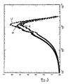
- the graph of figure 5 shows a comparative diagram reporting the pattern of the quality factor in function of the frequency of use for an integrate inductor of the known type and according to the present invention.
- the curve A shows the pattern of the quality factor in function of the frequency for inductors formed according to the prior art
- the curve B shows the pattern of the quality factor in function of the frequency for inductors formed according to the embodiment of figure 2
- the curve C shows the pattern of the quality factor in function of the frequency for inductors formed according to the embodiment of figure 3.
- testing data also confirms the improvement of the quality factor of inductors formed according to the invention.
- the insulating structures according to the invention can be formed in a simple substrate or in a SOI technology one.
- the resistive effect will be further increased if the insulating elements contact the buried oxide layer.
- a layer of photo sensible material is laid, in which a mask is defined by means of conventional photholitographic processes.
- an etching phase of the semiconductor layer 2 occurs so that a plurality of semiconductor elements separated from each other by the trenches formed in such substrate 2 is obtained.
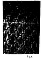
- Figure 6 is a picture, which is made with the electronic microscope, showing a substrate 2 portion of the embodiment of figure 3, at the end of such etching phase.
- an oxide layer is formed inside the trenches made in the substrate in order to form the insulating structure 4 of the inductive structure 1 according to the invention.
- the insulating structure 4 according to the invention comprises insulating elements 6, which are placed in a reciprocal spaced position and put in the substrate 2 according to a matrix.
- Such elements 6 can substantially have an annular shape.
- such elements 6 are connected to each other in order to form an insulating structure as a regular lattice.
- each element can be an annular one. There is nothing to prevent such insulating elements 6 can also having a different shape.
Landscapes
- Semiconductor Integrated Circuits (AREA)
Abstract
Description
- Figure 1 shows a vertical cross sectional view of a first embodiment of an inductive structure according to the invention;
- Figure 2 shows a top view of a second embodiment of an inductive structure according to the invention;
- Figure 3 shows a top view of a third embodiment of an inductive structure according to the invention;
- Figure 4 shows an enlarged scale top view of a substrate portion of the third embodiment of the inductive structure according to the invention;
- Figure 5 shows a comparative diagram between three inductive structures of the prior art and the embodiments according to the invention;
- Figure 6 shows a picture of a substrate portion of the inductive structure according to the invention.
- the formation of an oxide layer on the substrate portion where the
insulating
structure 4 is formed, - the formation of an
inductor 3 through a first or a second metalization layer.
Claims (8)
- Inductive structure (1) integrated in a semiconductor substrate (2), comprising at least a conductive element (3), which is insulated from the substrate (2), characterized in that it comprises an insulating structure (4), which is built inside said semiconductor substrate (2) and in correspondence with said conductive element (3), in order to increase the resistance of said substrate (2) and decrease the parasitic currents, which are induced in the substrate (2) by the conductive element.
- Inductive structure (1) integrated in a semiconductor substrate according to clam 1, characterized in that said insulating structure (4) comprises at least an insulating well (5), which is formed in the substrate (2).
- Inductive structure (1) integrated in a semiconductor substrate according to claim 1, characterized in that said insulating structure (4) comprises a plurality of insulating elements (6), which surround the semiconductor elements or silicon islands (2a) in the substrate (2).
- Inductive structure (1) integrated in a semiconductor substrate according to claim 3, characterized in that semiconductor elements or silicon islands (2a) are substantially patterned as mosaic tiles.
- Inductive structure (1) integrated in a semiconductor substrate according to claim 4, characterized in that said insulating elements (6) are separated from each other.
- Inductive structure (1) integrated in a semiconductor substrate according to claim 3, characterized in that said insulating elements (6) are interconnected with each other.
- Inductive structure (1) integrated in a semiconductor substrate according to any of the preceding claims, characterized in that the substrate (2) is formed with a SOI technology.
- Method to form inductive structures on a semiconductor substrate 2 comprising the following phases:depositing a layer of photosensitive material on the semiconductor substrate (2);defining a mask in said layer of photosensitive material by means of conventional photolithographic processes;etching the semiconductor substrate (2) through the mask in order to form a trench in the substrate (2) which surrounds islands or semiconductor elements (2a);filling said trench of insulating material in order to insulate, at least partially, islands or semiconductor elements (2a) and to form an insulating structure (4);forming an insulating layer on said insulating structure (4);forming a conductor element (3) to form the inductive element aligned with least one portion of the said inductive structure in order to reduce the parasitic currents induced by the conductor element (3) in the substrate (3).
Priority Applications (3)
| Application Number | Priority Date | Filing Date | Title |
|---|---|---|---|
| EP00830658A EP1195815B1 (en) | 2000-10-06 | 2000-10-06 | Inductive structure integrated on a semiconductor substrate |
| DE60035595T DE60035595D1 (en) | 2000-10-06 | 2000-10-06 | Inductive structure integrated on a semiconductor substrate |
| US09/972,766 US6580146B2 (en) | 2000-10-06 | 2001-10-05 | Inductive structure integrated on a semiconductor substrate |
Applications Claiming Priority (1)
| Application Number | Priority Date | Filing Date | Title |
|---|---|---|---|
| EP00830658A EP1195815B1 (en) | 2000-10-06 | 2000-10-06 | Inductive structure integrated on a semiconductor substrate |
Publications (2)
| Publication Number | Publication Date |
|---|---|
| EP1195815A1 true EP1195815A1 (en) | 2002-04-10 |
| EP1195815B1 EP1195815B1 (en) | 2007-07-18 |
Family
ID=8175504
Family Applications (1)
| Application Number | Title | Priority Date | Filing Date |
|---|---|---|---|
| EP00830658A Expired - Lifetime EP1195815B1 (en) | 2000-10-06 | 2000-10-06 | Inductive structure integrated on a semiconductor substrate |
Country Status (3)
| Country | Link |
|---|---|
| US (1) | US6580146B2 (en) |
| EP (1) | EP1195815B1 (en) |
| DE (1) | DE60035595D1 (en) |
Families Citing this family (3)
| Publication number | Priority date | Publication date | Assignee | Title |
|---|---|---|---|---|
| US7348666B2 (en) * | 2004-06-30 | 2008-03-25 | Endwave Corporation | Chip-to-chip trench circuit structure |
| US7411279B2 (en) * | 2004-06-30 | 2008-08-12 | Endwave Corporation | Component interconnect with substrate shielding |
| US7410894B2 (en) * | 2005-07-27 | 2008-08-12 | International Business Machines Corporation | Post last wiring level inductor using patterned plate process |
Citations (3)
| Publication number | Priority date | Publication date | Assignee | Title |
|---|---|---|---|---|
| US5874883A (en) * | 1995-07-18 | 1999-02-23 | Nec Corporation | Planar-type inductor and fabrication method thereof |
| US6054750A (en) * | 1995-12-22 | 2000-04-25 | Micron Technology, Inc. | Inductor formed at least partially in a substrate |
| US6093599A (en) * | 1997-12-27 | 2000-07-25 | Electronics And Telecomunications Research Institute | Method of manufacturing inductor device on a silicon substrate thereof |
Family Cites Families (1)
| Publication number | Priority date | Publication date | Assignee | Title |
|---|---|---|---|---|
| US6310387B1 (en) * | 1999-05-03 | 2001-10-30 | Silicon Wave, Inc. | Integrated circuit inductor with high self-resonance frequency |
-
2000
- 2000-10-06 DE DE60035595T patent/DE60035595D1/en not_active Expired - Lifetime
- 2000-10-06 EP EP00830658A patent/EP1195815B1/en not_active Expired - Lifetime
-
2001
- 2001-10-05 US US09/972,766 patent/US6580146B2/en not_active Expired - Lifetime
Patent Citations (3)
| Publication number | Priority date | Publication date | Assignee | Title |
|---|---|---|---|---|
| US5874883A (en) * | 1995-07-18 | 1999-02-23 | Nec Corporation | Planar-type inductor and fabrication method thereof |
| US6054750A (en) * | 1995-12-22 | 2000-04-25 | Micron Technology, Inc. | Inductor formed at least partially in a substrate |
| US6093599A (en) * | 1997-12-27 | 2000-07-25 | Electronics And Telecomunications Research Institute | Method of manufacturing inductor device on a silicon substrate thereof |
Also Published As
| Publication number | Publication date |
|---|---|
| US6580146B2 (en) | 2003-06-17 |
| US20020056888A1 (en) | 2002-05-16 |
| DE60035595D1 (en) | 2007-08-30 |
| EP1195815B1 (en) | 2007-07-18 |
Similar Documents
| Publication | Publication Date | Title |
|---|---|---|
| US5372967A (en) | Method for fabricating a vertical trench inductor | |
| JP3777159B2 (en) | High Q inductor | |
| US6310387B1 (en) | Integrated circuit inductor with high self-resonance frequency | |
| US5936298A (en) | Method for realizing magnetic circuits in an integrated circuit | |
| US5969590A (en) | Integrated circuit transformer with inductor-substrate isolation | |
| EP1374314B1 (en) | Integrated toroidal coil inductors for ic devices and manufacturing method | |
| US6166422A (en) | Inductor with cobalt/nickel core for integrated circuit structure with high inductance and high Q-factor | |
| US6373369B2 (en) | High efficiency thin film inductor | |
| KR100298480B1 (en) | Conductors for integrated circuits | |
| EP1267391B1 (en) | A method to fabricate RF inductors with minimum area | |
| KR20000011585A (en) | Semiconductor device and method for manufacturing the same | |
| KR19990055422A (en) | Inductor device on silicon substrate and manufacturing method thereof | |
| JPH08250332A (en) | Three-dimensional integrated circuit inductor | |
| US6292084B1 (en) | Fine inductor having 3-dimensional coil structure and method for producing the same | |
| EP1195815B1 (en) | Inductive structure integrated on a semiconductor substrate | |
| KR100938501B1 (en) | Inductor and its manufacturing method | |
| KR100685877B1 (en) | Semiconductor device and manufacturing method | |
| KR100880794B1 (en) | Inductor of semiconductor device and forming method thereof | |
| KR100709782B1 (en) | High Frequency Semiconductor Passive Device and Manufacturing Method Thereof | |
| JP2003086697A (en) | Semiconductor device | |
| JPH11135721A (en) | Inductor, method for manufacturing the same, and semiconductor integrated circuit device | |
| JPH11340420A (en) | Microwave semiconductor integrated circuit device | |
| KR19990053546A (en) | Method for manufacturing inductance element of semiconductor device | |
| HK1020297A (en) | Conductors for integrated circuits |
Legal Events
| Date | Code | Title | Description |
|---|---|---|---|
| PUAI | Public reference made under article 153(3) epc to a published international application that has entered the european phase |
Free format text: ORIGINAL CODE: 0009012 |
|
| AK | Designated contracting states |
Kind code of ref document: A1 Designated state(s): DE FR GB IT Kind code of ref document: A1 Designated state(s): AT BE CH CY DE DK ES FI FR GB GR IE IT LI LU MC NL PT SE |
|
| AX | Request for extension of the european patent |
Free format text: AL;LT;LV;MK;RO;SI |
|
| 17P | Request for examination filed |
Effective date: 20020411 |
|
| AKX | Designation fees paid |
Free format text: DE FR GB IT |
|
| 17Q | First examination report despatched |
Effective date: 20030415 |
|
| GRAP | Despatch of communication of intention to grant a patent |
Free format text: ORIGINAL CODE: EPIDOSNIGR1 |
|
| GRAS | Grant fee paid |
Free format text: ORIGINAL CODE: EPIDOSNIGR3 |
|
| GRAA | (expected) grant |
Free format text: ORIGINAL CODE: 0009210 |
|
| AK | Designated contracting states |
Kind code of ref document: B1 Designated state(s): DE FR GB IT |
|
| REG | Reference to a national code |
Ref country code: GB Ref legal event code: FG4D |
|
| REF | Corresponds to: |
Ref document number: 60035595 Country of ref document: DE Date of ref document: 20070830 Kind code of ref document: P |
|
| ET | Fr: translation filed | ||
| PG25 | Lapsed in a contracting state [announced via postgrant information from national office to epo] |
Ref country code: DE Free format text: LAPSE BECAUSE OF FAILURE TO SUBMIT A TRANSLATION OF THE DESCRIPTION OR TO PAY THE FEE WITHIN THE PRESCRIBED TIME-LIMIT Effective date: 20071019 |
|
| PLBE | No opposition filed within time limit |
Free format text: ORIGINAL CODE: 0009261 |
|
| STAA | Information on the status of an ep patent application or granted ep patent |
Free format text: STATUS: NO OPPOSITION FILED WITHIN TIME LIMIT |
|
| 26N | No opposition filed |
Effective date: 20080421 |
|
| GBPC | Gb: european patent ceased through non-payment of renewal fee |
Effective date: 20071018 |
|
| PG25 | Lapsed in a contracting state [announced via postgrant information from national office to epo] |
Ref country code: GB Free format text: LAPSE BECAUSE OF NON-PAYMENT OF DUE FEES Effective date: 20071018 |
|
| PGFP | Annual fee paid to national office [announced via postgrant information from national office to epo] |
Ref country code: IT Payment date: 20110924 Year of fee payment: 12 |
|
| PGFP | Annual fee paid to national office [announced via postgrant information from national office to epo] |
Ref country code: FR Payment date: 20121115 Year of fee payment: 13 |
|
| PG25 | Lapsed in a contracting state [announced via postgrant information from national office to epo] |
Ref country code: IT Free format text: LAPSE BECAUSE OF NON-PAYMENT OF DUE FEES Effective date: 20121006 |
|
| REG | Reference to a national code |
Ref country code: FR Ref legal event code: ST Effective date: 20140630 |
|
| PG25 | Lapsed in a contracting state [announced via postgrant information from national office to epo] |
Ref country code: FR Free format text: LAPSE BECAUSE OF NON-PAYMENT OF DUE FEES Effective date: 20131031 |