EP1195771A2 - Differential voltage sense circuit to detect the state of a CMOS process compatible fuses at low supply voltages - Google Patents
Differential voltage sense circuit to detect the state of a CMOS process compatible fuses at low supply voltages Download PDFInfo
- Publication number
- EP1195771A2 EP1195771A2 EP01000514A EP01000514A EP1195771A2 EP 1195771 A2 EP1195771 A2 EP 1195771A2 EP 01000514 A EP01000514 A EP 01000514A EP 01000514 A EP01000514 A EP 01000514A EP 1195771 A2 EP1195771 A2 EP 1195771A2
- Authority
- EP
- European Patent Office
- Prior art keywords
- differential voltage
- sense circuit
- fuse
- circuit according
- voltage
- Prior art date
- Legal status (The legal status is an assumption and is not a legal conclusion. Google has not performed a legal analysis and makes no representation as to the accuracy of the status listed.)
- Granted
Links
Images

Classifications
-
- G—PHYSICS
- G01—MEASURING; TESTING
- G01R—MEASURING ELECTRIC VARIABLES; MEASURING MAGNETIC VARIABLES
- G01R19/00—Arrangements for measuring currents or voltages or for indicating presence or sign thereof
-
- G—PHYSICS
- G11—INFORMATION STORAGE
- G11C—STATIC STORES
- G11C17/00—Read-only memories programmable only once; Semi-permanent stores, e.g. manually-replaceable information cards
- G11C17/14—Read-only memories programmable only once; Semi-permanent stores, e.g. manually-replaceable information cards in which contents are determined by selectively establishing, breaking or modifying connecting links by permanently altering the state of coupling elements, e.g. PROM
- G11C17/16—Read-only memories programmable only once; Semi-permanent stores, e.g. manually-replaceable information cards in which contents are determined by selectively establishing, breaking or modifying connecting links by permanently altering the state of coupling elements, e.g. PROM using electrically-fusible links
-
- G—PHYSICS
- G11—INFORMATION STORAGE
- G11C—STATIC STORES
- G11C7/00—Arrangements for writing information into, or reading information out from, a digital store
- G11C7/06—Sense amplifiers; Associated circuits, e.g. timing or triggering circuits
- G11C7/062—Differential amplifiers of non-latching type, e.g. comparators, long-tailed pairs
-
- G—PHYSICS
- G11—INFORMATION STORAGE
- G11C—STATIC STORES
- G11C7/00—Arrangements for writing information into, or reading information out from, a digital store
- G11C7/06—Sense amplifiers; Associated circuits, e.g. timing or triggering circuits
- G11C7/065—Differential amplifiers of latching type
Definitions
- This invention relates generally to differential fuse sensing circuits, and more particularly to a differential voltage sense circuit to detect the state of a CMOS process compatible (e.g., silicide poly, doped poly, metal) fuse at low power supply voltages.
- the state of the fuse can be either blown (e.g., open or resistance greater than 1 M ⁇ ) or not blown (e.g., short or resistance less than 100 ⁇ ).
- Non-volatile memory In the fabrication of electrical circuits, especially those formed in semiconductor integrated circuits, a non-volatile memory element is necessary to retain stored information when the power to the device is turned off.
- Non-volatile memory has traditionally been ROM, ePROM, and eePROM.
- ROM is not general because it requires mask level programming at the factor.
- Memory made from ePROM or eePROM are very general purpose but require additional special process steps to have this storage element. Also, in the latest CMOS processes, the gate oxides are so thin that the charge used to store the bit can leak (tunnel) out. Fuses are another type of non-volatile memory which do not require any special process additions.
- fuse There are two types of fuse; laser fuses (usually metal links that are zapped by a laser to open them at the factory before packaging), and the type considered for this invention called poly fuses (even though the fuse material may be metal or silicide poly, etc.) which can be programmed once in the package.
- laser fuses usually metal links that are zapped by a laser to open them at the factory before packaging
- poly fuses even though the fuse material may be metal or silicide poly, etc.
- fuses are used include chip ID, repair of large SRAM's by enabling redundant rows or columns, or trimming the process variations out of resistors and/or capacitors to make precise components used in analog-to-digital (A/D) and digital-to-analog (D/A) converters.
- A/D analog-to-digital
- D/A digital-to-analog
- a fuse may be used to selectively connect additional elements to create the desired output for an analog circuit needing more precision than the process is capable of delivering.
- fuses Since the fuses are programmed in the package, a transistor decoder is required and the fusing current is limited. As a result, fuses may be only partially blown, i.e., neither open nor short. This ambiguity creates a situation in which indeterminate logic outputs may be created thereby rendering the circuit useless (or at least less useful).
- Prior art current sensing circuits can not determine if the fuse is blown at some of the voltage, process and temperature corners at low supply voltages for scaled CMOS processes. This is because known circuit topologies are problematic at low supply voltage and at low current levels.
- Conventional current sensing circuits use a current subtracter followed by resistive loaded common-source amplifiers to gain up the signal, but the gain is proportional to the supply voltage which means that as the supply voltage is reduced, the gain decreases. This characteristic renders such circuits incapable of functioning over the 0.6V to 2.5V supply voltage range of advanced CMOS processes (e.g., deep sub-micron processes such as the 0.13um or 0.10um technology nodes and beyond).
- CMOS process compatible e.g., silicide poly, doped poly, metal
- the present invention is directed to a differential voltage sense circuit to determine the state of CMOS process compatible (e.g., silicide poly) fuses at low power supply voltages.
- the voltage sense circuit uses a differential voltage scheme based on a resistance bridge and differential latch circuit that is designed for low voltage operation.
- the bridge is very sensitive to changes in the resistance in one arm. This difference is sensed, gained up (amplified) and latched in one circuit.
- a differential voltage sense circuit comprising a resistance bridge having two upper legs and two lower legs.
- One upper leg includes a CMOS process compatible fuse and the other upper leg includes a CMOS process compatible resistor.
- Each lower leg includes a CMOS process compatible switch selected from a pair of matching switches.
- the sense circuit has a comparator for sensing a voltage difference between the two legs where the upper and lower legs are joined together.
- the sense circuit further has a latch for latching a voltage having a state determined by the voltage difference and that is indicative of the state of the resistor fuse.
- the sense circuit further has a combinational element for preventing the bridge switches from turning off and stopping the flow of current through the resistance bridge until after the fuse state (status) information is latched by the latch.
- a differential voltage sense circuit is implemented that has virtually infinite gain (due to positive feedback) at a desired decision point.
- a differential voltage sense circuit is implemented that is very efficient.
- a differential voltage sense circuit is implemented to detect the state of silicide poly fuses at low power supply voltages.
- a differential voltage sense circuit is implemented that is compatible with advanced CMOS processes.
- a differential voltage sense circuit is implemented that works for the entire voltage supply range that the CMOS logic gates work, all process corners and about -40°C to about 125°C temperatures for all the deep sub-micron processes.
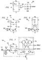
- Figure 1(a) illustrates a prior art differential current sensing circuit 10 that senses the difference in a reference current and the fuse current.
- the current that flows through the sense resistor Rs 12 is differenced (i.e. compared) with the current flowing through the fuse 13, via the current mirror M1-M2 at node 'A' 14. If the fuse 13 is not blown, then its resistance is much less than Rs 12 and the current through the fuse will be much greater so that node 'A' 14 will be pulled near Vss in value.
- DATAOUT 16 will also be at or near ground (Vss) after node 'A' 14 is gained up by the two common-source amplifiers M3 and M4.
- the circuit 100 depicted in Figure 1(b) simplifies the circuit 10 of Figure 1(a) by eliminating the extra bias leg and current source 18 by making the PMOS transistor gates 102 controlled by a signal READ 104.
- READ 104 control line When READ 104 control line is low, then the cell 100 will sense the fuse 13 condition since the PMOS transistors will be "ON” and conducting current. The state of the PMOS transistors will be in triode condition and have low resistance if their Width/Length (W/L) ratio is made large.
- W/L Width/Length
- the fuse cell 100 information at DATAOUT 16 is lost when READ 104 is high; therefore a D-latch is required to follow the fuse cell 100 to hold the information.
- the circuit 100 shown in Figure 1(b) was found by the present inventors to work well down to the 2.5V mode, but to be insufficient for 1.5V and 1.2V advanced CMOS technologies.
- the insufficiencies were attributed substantially to large mismatches in the M1-M2 current mirror, large output conductance variation in the transistors which causes the gain to vary, and the fact that the common-source amplifiers, M3 and M4, are resistively loaded.
- resistors 304 are chosen to be somewhere between the foregoing extremes, such as 20k ⁇ , then the delta voltage 307 is found to be 0.409V DD for a blown fuse 302 and 0.495V DD for a good fuse 302. This then is the magnitude of the delta. The sign of the delta voltage 307 was also found to change from not blown to blown; and this information then is the information that must be logically encoded. This task could be achieved using a differential amplifier 402 and a latch 404 as illustrated in the voltage sensing circuit 400 depicted in Figure 4.
- Triode NMOS devices 306 therefore can be used to act as resistors when "ON” and can be turned “OFF” to stop the current flow when the data has been stored.
- the voltage sense bridge circuit 600 illustrated in Figure 6, for example, can be used to achieve the desired goals.
- the NMOS transistors 306 are designed to have a narrow width and a long channel length to act as good resistors when turned "ON” (READ 506 is high).
- the NMOS transistors 306 most preferably are matched so they have identical electrical characteristics. This feature will reduce the amount of wafer area necessary to implement the circuit 600. It will be appreciated that choosing the size of the two NMOS devices 306 properly will cause the circuit 600 to function in the same manner as the circuit 300 described herein before. It can also be appreciated that any comparator that senses the delta voltage 307 may have to be more sensitive, but the requisite sensitivity can be easily implemented with a well designed comparator.
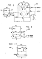
- Figure 7 illustrates a differential voltage sense circuit 700 comprising a very small latch 702 having high gain and that uses very little to no current when in the data holding mode of operation. It can be seen that the latch 702 is embedded into the loads of the comparator input pair 704. When READ 104 is low, the current flows in the bridge and the delta voltage 307 builds up at the input gates of M3 (704) and M4 (704). When READ 104 transitions high, the latching comparator transistors 704 are enabled and operate to amplify the delta voltage 307 until the regenerative latch 702 flips and stores the data. The inverter 708 is required to have a slow falling edge so that the current in the bridge 706 does not stop flowing and destroy the delta voltage 307 before the latch 702 trips.
- the present inventors further recognized the possibility of a race condition that can occur with the differential voltage sense circuit 700 under some conditions of temperature, process and supply voltage ranges. These issues are resolved with the differential voltage sense circuit 800 illustrated in Figure 8.
- the circuit 800 is guaranteed to latch the data before transistors 306 are turned off by NOR gate 802.
- the differential voltage sense circuit 800 is considered by the inventors to be the a preferred embodiment of the present invention. It is especially preferred that resistor 304 be constructed of non-silicide, doped poly silicon which is the standard gate material in all CMOS processes. Another preferred material for use in a CMOS process comprises the doped silicon that forms the N-well or P-well region, depending on the type of process employed.
- Figure 9 illustrates a differential voltage sense circuit resistance bridge 900 that operates to protect damage to the gate oxide of the transistors 306 in the lower leg of the bridge 900 due to the large voltage transition used to blow the fuse.
- the present inventors recognized that when a fuse 302 is blown, the supply voltage is increased such that the input gates of the comparator transistors M3 and M4 shown in Figure 8 may experience a large enough transition voltage to harm the gate oxide.
- the PMOS devices 902 turn-off when the fuse 302 is being blown, therefore isolating the high voltage from any gate oxide.
- FIG 10 illustrates a differential voltage sense circuit resistance bridge 1000 according to another embodiment of the present invention.
- resistor 304 in differential voltage sense circuit 800 can be replaced with the PMOS transistor 1002 having a narrow width and a long channel to retain the requisite resistor characteristics. Parametric variations will of course be much higher for a differential voltage sense circuit using the bridge 1000 when compared with use of a bridge using a resistor 304 constructed from poly silicon or N-well silicon, as discussed herein before. More care must therefore be taken in the design of the comparator/latch 702, 704 that senses the delta voltage 307.
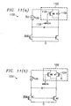
- Figure 11(a) illustrates a differential voltage sense circuit resistance bridge 1100 comprising a structure 1102 to lower the value of the impedance in the sense arm of the bridge 1100 according to an embodiment of the present invention.
- the present inventors recognized that although factory testing can be implemented to detect the state of a blown fuse for a given differential voltage sense circuit, aging characteristics associated with fuse values may cause the sense circuit to fail over time. Also, the operational conditions in the field may be degraded such as decreased supply voltage or elevated temperature that can not be completely tested for at the factory.
- the PMOS transistor 1104 is used to lower the value of the impedance 1106 in the sense arm of the bridge 1100.
- Deployment of the structure 1102 would be as follows: During testing at the factory, PMOS device 1104 is turned “OFF" and the fuse 302 is determined to be blown with a larger value for impedance 1106. This means that the resistance of fuse 302 is much larger than that of impedance 1106. In the field, a MARGIN signal 1108 is generated causing PMOS transistor 1104 to reduce the value of impedance 1106 such that it further deviates from the fuse 302 resistance value. In this way, the resistance value of the fuse 302 can "regrow” a defined amount while permitting the differential voltage sense circuit to remain functional. This modification also covers the changes in environmental conditions and allows for continued functional operation of the circuit.
- FIG 11(b) illustrates a differential voltage sense circuit resistance bridge 1200 comprising a structure 1202 to lower the value of the impedance in the sense arm of the bridge according to another embodiment of the present invention.
- the bridge 1200 functions similar to the bridge described above with reference to Figure 11(a), except a PMOS device 1204 operates as the impedance setting device in the sensing arm of the resistance bridge 1200.
- the circuit is described as a bridge with the fuse and sense resistor in the upper arms, but clearly this idea is the same if the fuse and sense resistor were in the lower arms and PMOS devices were used as matched resistances for the upper arms of the bridge.
- the CMOS differential amp/latch would be modified by changing all NMOS transistors to PMOS and visa versa.
- the logic sense would also be inverted.
- the present invention presents a significant advancement in the art of sense technology to detect the state of CMOS fuses at low power supply voltages. Further, this invention has been described in considerable detail in order to provide those skilled in the data communication art with the information needed to apply the novel principles and to construct and use such specialized components as are required. In view of the foregoing descriptions, it should further be apparent that the present invention represents a significant departure from the prior art in construction and operation. However, while particular embodiments of the present invention have been described herein in detail, it is to be understood that various alterations, modifications and substitutions can be made therein without departing in any way from the spirit and scope of the present invention.
- a differential voltage sense circuit having the following features: (i) a resistance bridge having a fused upper leg, a resistive upper leg, a first switched lower leg connected to the fused upper leg and a second switched lower leg connected to the resistive upper leg; (ii) a comparator for sensing a voltage difference between the first and second switched lower legs of the resistance bridge where the upper legs join with the lower legs; (iii) a latch for latching voltage state information associated with the voltage difference; and (iv) a combinational element for preventing the switched lower legs of the resistance bridge from turning off until the voltage state information is latched.
- the fused upper leg may be poly silicide fuse.
- the resistive upper leg may be a CMOS process doped silicon N-well or P-well, or a poly silicide resistor.
- the comparator preferably operable for sensing the voltage difference in response to a read signal.
- the combinational element may be a NOR gate.
- the resistance bridge, comparator, latch and combinational element should be compatible with deep sub-micron CMOS processes.
- Each lower leg of the resistance bridge may comprise an isolation device for isolating high switching voltage levels from the comparator.
- the resistive upper leg of the resistance bridge may solely comprises a CMOS transistor or solely comprises a resistor.
- the resistive upper leg of the resistance bridge may be a controlled impedance that comprises a resistor and a CMOS transistor operable for varying the impedance of the resistor in response to a margin signal.
- the controlled impedance may comprise a first CMOS transistor configured as a resistor and a second CMOS transistor operable for varying the impedance of the first CMOS transistor in response to a margin signal.
- a differential voltage sense circuit comprises the following features: (i) a resistance bridge having at least one fused leg connected to a supply voltage; (ii) means for sensing a voltage difference associated with the resistance bridge, wherein the voltage difference has a polarity that is indicative of fuse status information; and (iii) means for latching the fuse status information.
- the fused leg comprises a silicide poly fuse and the resistance bridge further has a sense leg connected to the supply voltage.
- the sense leg comprises a silicide poly resistor or a controlled impedance that includes a resistor and a CMOS transistor that are operable to vary the impedance of the sense element in response to a control signal.
- the controlled impedance comprises a first CMOS transistor configured as an impedance device and a second CMOS transistor operational to vary the impedance of the first CMOS transistor in response to a control signal.
- the resistance bridge further has a pair of switch element legs connected to a common ground.
- the fused leg comprises a silicide poly fuse.
- Each switch element leg comprises a CMOS switch, wherein the CMOS switches have matching switching characteristics.
- Each switch element leg of the resistance bridge further comprises an isolation device operational to isolate high switching voltage levels from the sensing means.
- the sensing means comprises a voltage comparator.
- a combinational element may also be provided that is operable to maintain the voltage difference until the fuse status information is latched.
- the combinational element may bea NOR gate.
Landscapes
- Physics & Mathematics (AREA)
- General Physics & Mathematics (AREA)
- Design And Manufacture Of Integrated Circuits (AREA)
- Read Only Memory (AREA)
- Semiconductor Integrated Circuits (AREA)
- For Increasing The Reliability Of Semiconductor Memories (AREA)
- Tests Of Electronic Circuits (AREA)
- Static Random-Access Memory (AREA)
- Control Of Voltage And Current In General (AREA)
- Fuses (AREA)
Abstract
Description

Claims (20)
- A differential voltage sense circuit comprising:a resistance bridge having a fuse in one upper leg, a sense element in its other upper leg, and a switch in each lower leg, the upper legs connected to a common supply voltage, wherein the bridge is operable for generating a differential voltage in response to a switch input signal common to both switches that causes current to flow through both switches, the fuse and the sense element, wherein the differential voltage has a polarity that provides fuse status information; anda latch for storing the fuse status information.
- The differential voltage sense circuit according to claim 1 further comprising:a comparator for sensing the differential voltage and for generating the fuse status information in response to an input signal that initiates the switch input signal.
- The differential voltage sense circuit according to claim 2, wherein the resistance bridge, comparator, and latch are capable of operating at a supply voltage compatible with deep sub-micron CMOS processes.
- The differential voltage sense circuit according to claim 2 further comprising:a combinational element operable for causing the switch current to flow until the fuse status information is latched.
- The differential voltage sense circuit according to claim 4, wherein the combinational element comprises a NOR gate.
- The differential voltage sense circuit according to claim 4, wherein the resistance bridge, comparator, latch and combinational element are capable of operating at a supply voltage compatible with deep sub-micron CMOS processes.
- The differential voltage sense circuit according to claim 1, wherein the fuse comprises a silicide poly fuse.
- The differential voltage sense circuit according to claim 1, wherein the sense element comprises a silicide poly resistor.
- The differential voltage sense circuit according to claim 1, wherein the sense element comprises a CMOS process doped silicon N-well.
- The differential voltage sense circuit according to claim 1, wherein the sense element comprises a CMOS process doped silicon P-well.
- The differential voltage sense circuit according to claim 1, wherein each lower leg of the resistance bridge further comprises an isolation device for isolating high switching voltage levels from the comparator.
- The differential voltage sense circuit according to claim 1, wherein the sense element solely comprises a CMOS transistor.
- The differential voltage sense circuit according to claim 1, wherein the sense element solely comprises a resistor.
- The differential voltage sense circuit according to claim 1, wherein the sense element solely comprises a controlled impedance.
- The differential voltage sense circuit according to claim 14, wherein the controlled impedance comprises a resistor and a CMOS transistor that are operable to vary the impedance of the sense element in response to a margin signal.
- The differential voltage sense circuit according to claim 14, wherein the controlled impedance comprises a first CMOS transistor configured as an impedance device and a second CMOS transistor and that are operable to vary the impedance of the first CMOS transistor in response to a margin signal.
- A method of determining CMOS process compatible fuse status information comprising the steps of:(a) providing a voltage supply having a voltage compatible with deep sub-micron CMOS processes;(b) connecting a resistance bridge to the supply voltage and having a fuse in at least one leg of the resistance bridge;(c) generating a voltage difference between two legs of the resistance bridge such that a polarity associated with the voltage difference provides fuse status information in response to a first input signal; and(d) latching the fuse status information.
- The method according to claim 17 further comprising the step of:sensing the voltage difference in response to a second input signal and generating the fuse status information therefrom prior to latching the fuse status information.
- The method according to claim 18 further comprising the step of:sensing the latched fuse status information and generating the first input signal therefrom.
- The method according to claim 19 further comprising the step of:removing the first input signal such that current no longer flows in the resistance bridge subsequent to latching the fuse status information.
Applications Claiming Priority (2)
| Application Number | Priority Date | Filing Date | Title |
|---|---|---|---|
| US09/680,811 US6384664B1 (en) | 2000-10-05 | 2000-10-05 | Differential voltage sense circuit to detect the state of a CMOS process compatible fuses at low power supply voltages |
| US680811 | 2000-10-05 |
Publications (3)
| Publication Number | Publication Date |
|---|---|
| EP1195771A2 true EP1195771A2 (en) | 2002-04-10 |
| EP1195771A3 EP1195771A3 (en) | 2002-05-29 |
| EP1195771B1 EP1195771B1 (en) | 2005-01-12 |
Family
ID=24732610
Family Applications (1)
| Application Number | Title | Priority Date | Filing Date |
|---|---|---|---|
| EP01000514A Expired - Lifetime EP1195771B1 (en) | 2000-10-05 | 2001-10-02 | Differential voltage sense circuit to detect the state of CMOS process compatible fuses at low supply voltages |
Country Status (7)
| Country | Link |
|---|---|
| US (1) | US6384664B1 (en) |
| EP (1) | EP1195771B1 (en) |
| JP (1) | JP2002208296A (en) |
| KR (1) | KR100864741B1 (en) |
| AT (1) | ATE287120T1 (en) |
| DE (1) | DE60108328T2 (en) |
| TW (1) | TW563129B (en) |
Cited By (4)
| Publication number | Priority date | Publication date | Assignee | Title |
|---|---|---|---|---|
| WO2007118679A1 (en) * | 2006-04-13 | 2007-10-25 | Austriamicrosystems Ag | Circuit arrangement comprising a non-volatile memory cell, and method |
| WO2008028853A1 (en) * | 2006-09-07 | 2008-03-13 | Austriamicrosystems Ag | Circuit configuration, and method for the operation of a circuit configuration |
| EP1800323A4 (en) * | 2004-09-01 | 2008-11-26 | Ibm | ELECTRONICALLY PROGRAMMABLE LOW VOLTAGE FUSE HAVING A DIFFERENTIAL DETECTION SCHEME |
| CN105759369A (en) * | 2014-12-19 | 2016-07-13 | 华为技术有限公司 | Laser leakage-preventing optical module and control method |
Families Citing this family (55)
| Publication number | Priority date | Publication date | Assignee | Title |
|---|---|---|---|---|
| US6859090B2 (en) * | 2002-01-31 | 2005-02-22 | Agere Systems Inc. | Buried fuse reading device |
| WO2003096353A1 (en) * | 2002-05-08 | 2003-11-20 | Semtech Corporation | Method and apparatus for improving the reliability of the reading of integrated circuit fuses |
| US6710640B1 (en) * | 2002-09-19 | 2004-03-23 | Infineon Technologies Ag | Active well-bias transistor for programming a fuse |
| US6819144B2 (en) * | 2003-03-06 | 2004-11-16 | Texas Instruments Incorporated | Latched sense amplifier with full range differential input voltage |
| US6765825B1 (en) | 2003-03-12 | 2004-07-20 | Ami Semiconductor, Inc. | Differential nor memory cell having two floating gate transistors |
| US6873543B2 (en) * | 2003-05-30 | 2005-03-29 | Hewlett-Packard Development Company, L.P. | Memory device |
| US6995601B2 (en) * | 2004-01-14 | 2006-02-07 | Taiwan Semiconductor Manufacturing Co., Ltd. | Fuse state detection circuit |
| US7019534B2 (en) * | 2004-03-26 | 2006-03-28 | Taiwan Semiconductor Manufacturing Co., Ltd. | Detecting the status of an electrical fuse |
| US7084696B2 (en) * | 2004-04-07 | 2006-08-01 | International Business Machines Corporation | Circuits associated with fusible elements for establishing and detecting of the states of those elements |
| JP4282529B2 (en) * | 2004-04-07 | 2009-06-24 | 株式会社東芝 | Semiconductor integrated circuit device and program method thereof |
| US6972614B2 (en) * | 2004-04-07 | 2005-12-06 | International Business Machines Corporation | Circuits associated with fusible elements for establishing and detecting of the states of those elements |
| US7459956B2 (en) * | 2004-05-05 | 2008-12-02 | Taiwan Semiconductor Manufacturing Co., Ltd. | Storing information with electrical fuse for device trimming |
| US7009443B2 (en) * | 2004-06-07 | 2006-03-07 | Standard Microsystems Corporation | Method and circuit for fuse programming and endpoint detection |
| JP2006059429A (en) * | 2004-08-19 | 2006-03-02 | Matsushita Electric Ind Co Ltd | Semiconductor memory device |
| US7215175B1 (en) * | 2004-09-01 | 2007-05-08 | Sun Microsystems, Inc. | Fuse sensing scheme with auto current reduction |
| US7342836B2 (en) * | 2004-09-24 | 2008-03-11 | Cypress Semiconductor Corporation | One time programmable latch and method |
| JP4646608B2 (en) * | 2004-11-26 | 2011-03-09 | パナソニック株式会社 | Semiconductor memory device |
| DE102005009050B4 (en) * | 2005-02-28 | 2007-01-11 | Infineon Technologies Ag | Differential readout circuit for fuse memory cells |
| US20060232904A1 (en) * | 2005-04-13 | 2006-10-19 | Taiwan Semiconductor Manufacturing Co. | Supply voltage independent sensing circuit for electrical fuses |
| US7236023B2 (en) | 2005-04-14 | 2007-06-26 | Sandisk 3D Llc | Apparatus and methods for adaptive trip point detection |
| US7233539B2 (en) * | 2005-05-24 | 2007-06-19 | Freescale Semiconductor, Inc. | Non-volatile fuse circuit |
| US7242239B2 (en) * | 2005-06-07 | 2007-07-10 | International Business Machines Corporation | Programming and determining state of electrical fuse using field effect transistor having multiple conduction states |
| KR100691349B1 (en) * | 2005-07-20 | 2007-03-12 | 삼성전자주식회사 | Differential Circuits, Output Buffer Circuits, and Semiconductor Integrated Circuits Used in Multi-Power Systems |
| US8072834B2 (en) | 2005-08-25 | 2011-12-06 | Cypress Semiconductor Corporation | Line driver circuit and method with standby mode of operation |
| US7304527B1 (en) * | 2005-11-30 | 2007-12-04 | Altera Corporation | Fuse sensing circuit |
| US7760536B2 (en) * | 2006-04-25 | 2010-07-20 | Freescale Semiconductor, Inc. | Non-volatile memory cell |
| US7327595B2 (en) * | 2006-05-09 | 2008-02-05 | Analog Devices, Inc. | Dynamically read fuse cell |
| US7528646B2 (en) * | 2006-10-19 | 2009-05-05 | International Business Machines Corporation | Electrically programmable fuse sense circuit |
| US7821859B1 (en) | 2006-10-24 | 2010-10-26 | Cypress Semiconductor Corporation | Adaptive current sense amplifier with direct array access capability |
| US7501879B1 (en) | 2007-03-13 | 2009-03-10 | Xilinx, Inc. | eFuse resistance sensing scheme with improved accuracy |
| JP5283975B2 (en) * | 2007-06-07 | 2013-09-04 | ルネサスエレクトロニクス株式会社 | Semiconductor memory device and data writing method and data reading method thereof |
| US7495987B2 (en) * | 2007-06-11 | 2009-02-24 | Freescale Semiconductor, Inc. | Current-mode memory cell |
| US7701226B2 (en) * | 2007-07-03 | 2010-04-20 | Kabushiki Kaisha Toshiba | Systems and methods for determining the state of a programmable fuse in an IC |
| US20090039462A1 (en) * | 2007-08-07 | 2009-02-12 | Mediatek Inc. | Efuse devices and efuse arrays thereof and efuse blowing methods |
| US7550323B2 (en) * | 2007-08-08 | 2009-06-23 | International Business Machines Corporation | Electrical fuse with a thinned fuselink middle portion |
| US20090040006A1 (en) * | 2007-08-08 | 2009-02-12 | International Business Machines Corporation | Electrical fuse with enhanced programming current divergence |
| US20090079439A1 (en) * | 2007-09-20 | 2009-03-26 | United Microelectronics Corp. | Efuse system and testing method thereof |
| JP2009087453A (en) * | 2007-09-28 | 2009-04-23 | Sanyo Electric Co Ltd | Information storage circuit |
| US7838963B2 (en) * | 2007-10-26 | 2010-11-23 | International Business Machines Corporation | Electrical fuse having a fully silicided fuselink and enhanced flux divergence |
| US7742352B1 (en) | 2007-10-30 | 2010-06-22 | Silicon Laboratories Inc. | Variable sense level for fuse-based non-volatile memory |
| US7724600B1 (en) | 2008-03-05 | 2010-05-25 | Xilinx, Inc. | Electronic fuse programming current generator with on-chip reference |
| KR100968894B1 (en) * | 2008-07-21 | 2010-07-14 | 로얄금속공업 주식회사 | Cases for beauty instruments |
| DE102008048830B4 (en) * | 2008-09-25 | 2010-11-04 | Austriamicrosystems Ag | Circuit arrangement with fuse and method for determining a state of a fuse |
| US7960809B2 (en) * | 2009-01-16 | 2011-06-14 | International Business Machines Corporation | eFuse with partial SiGe layer and design structure therefor |
| JP2010233140A (en) | 2009-03-30 | 2010-10-14 | Hitachi Ltd | Semiconductor integrated circuit device |
| KR101123074B1 (en) * | 2009-04-30 | 2012-03-05 | 주식회사 하이닉스반도체 | Fuse circuit and semiconductor device including the same |
| US8248079B2 (en) * | 2009-09-21 | 2012-08-21 | Nanya Technology Corporation | Sensing circuit for sensing electric fuse and sensing method thereof |
| US8957694B2 (en) * | 2012-05-22 | 2015-02-17 | Broadcom Corporation | Wafer level package resistance monitor scheme |
| CN106160744A (en) * | 2016-07-07 | 2016-11-23 | 合肥工业大学 | A kind of high speed dynamic latch comparator applied in low voltage environment |
| US20180061507A1 (en) * | 2016-08-29 | 2018-03-01 | Skyworks Solutions, Inc. | Fuse state sensing circuits, devices and methods |
| CN106708155B (en) * | 2016-11-22 | 2017-12-26 | 成都芯源系统有限公司 | Integrated circuit and circuit characteristic adjusting method thereof |
| CN109256158A (en) * | 2018-08-16 | 2019-01-22 | 歌尔股份有限公司 | sensing circuit |
| CN110995215B (en) * | 2019-12-16 | 2023-08-29 | 北京时代民芯科技有限公司 | Gain-adjustable high-speed high-precision comparator circuit |
| US11742012B2 (en) | 2021-05-28 | 2023-08-29 | Nxp Usa, Inc. | Memory read circuitry with a flipped voltage follower |
| CN117405267A (en) * | 2023-10-18 | 2024-01-16 | 苏州锐光科技有限公司 | MEMS piezoresistive pressure sensor |
Family Cites Families (14)
| Publication number | Priority date | Publication date | Assignee | Title |
|---|---|---|---|---|
| US4995004A (en) * | 1989-05-15 | 1991-02-19 | Dallas Semiconductor Corporation | RAM/ROM hybrid memory architecture |
| JPH05101697A (en) * | 1991-10-02 | 1993-04-23 | Nec Corp | Fault diagnostic circuit for lsi |
| JP2554816B2 (en) * | 1992-02-20 | 1996-11-20 | 株式会社東芝 | Semiconductor memory device |
| US5536968A (en) * | 1992-12-18 | 1996-07-16 | At&T Global Information Solutions Company | Polysilicon fuse array structure for integrated circuits |
| US5404049A (en) * | 1993-11-02 | 1995-04-04 | International Business Machines Corporation | Fuse blow circuit |
| US5587037A (en) * | 1994-11-23 | 1996-12-24 | Custom Graphics | Multi-layer sheet material having a refractive surface and method for making same |
| US5731733A (en) * | 1995-09-29 | 1998-03-24 | Intel Corporation | Static, low current sensing circuit for sensing the state of a fuse device |
| US5976943A (en) * | 1996-12-27 | 1999-11-02 | Vlsi Technology, Inc. | Method for bi-layer programmable resistor |
| US5920771A (en) * | 1997-03-17 | 1999-07-06 | Gennum Corporation | Method of making antifuse based on silicided single polysilicon bipolar transistor |
| US6091273A (en) * | 1997-08-19 | 2000-07-18 | International Business Machines Corporation | Voltage limiting circuit for fuse technology |
| KR100287541B1 (en) * | 1998-05-29 | 2001-04-16 | 윤종용 | Redundancy decoder enable circuit of semiconductor memory device |
| JP2000200497A (en) * | 1998-11-05 | 2000-07-18 | Nec Corp | Fuse determination circuit and memory redundancy setting circuit |
| US6157583A (en) * | 1999-03-02 | 2000-12-05 | Motorola, Inc. | Integrated circuit memory having a fuse detect circuit and method therefor |
| US6525397B1 (en) * | 1999-08-17 | 2003-02-25 | National Semiconductor Corporation | Extended drain MOSFET for programming an integrated fuse element to high resistance in low voltage process technology |
-
2000
- 2000-10-05 US US09/680,811 patent/US6384664B1/en not_active Expired - Lifetime
-
2001
- 2001-10-02 DE DE60108328T patent/DE60108328T2/en not_active Expired - Lifetime
- 2001-10-02 AT AT01000514T patent/ATE287120T1/en not_active IP Right Cessation
- 2001-10-02 EP EP01000514A patent/EP1195771B1/en not_active Expired - Lifetime
- 2001-10-04 KR KR1020010061136A patent/KR100864741B1/en not_active Expired - Fee Related
- 2001-10-05 JP JP2001309432A patent/JP2002208296A/en active Pending
- 2001-10-05 TW TW090124696A patent/TW563129B/en not_active IP Right Cessation
Cited By (8)
| Publication number | Priority date | Publication date | Assignee | Title |
|---|---|---|---|---|
| EP1800323A4 (en) * | 2004-09-01 | 2008-11-26 | Ibm | ELECTRONICALLY PROGRAMMABLE LOW VOLTAGE FUSE HAVING A DIFFERENTIAL DETECTION SCHEME |
| WO2007118679A1 (en) * | 2006-04-13 | 2007-10-25 | Austriamicrosystems Ag | Circuit arrangement comprising a non-volatile memory cell, and method |
| GB2449609A (en) * | 2006-04-13 | 2008-11-26 | Austriamicrosystems Ag | Circuit arrangement comprising a non-volatile memory cell, and method |
| US7995367B2 (en) | 2006-04-13 | 2011-08-09 | Austriamicrosystems Ag | Circuit arrangement comprising a non-volatile memory cell and method |
| WO2008028853A1 (en) * | 2006-09-07 | 2008-03-13 | Austriamicrosystems Ag | Circuit configuration, and method for the operation of a circuit configuration |
| CN105759369A (en) * | 2014-12-19 | 2016-07-13 | 华为技术有限公司 | Laser leakage-preventing optical module and control method |
| CN105759369B (en) * | 2014-12-19 | 2018-03-09 | 华为技术有限公司 | Prevent the optical module and control method that laser is revealed |
| US10008824B2 (en) | 2014-12-19 | 2018-06-26 | Huawei Technologies Co., Ltd. | Optical module for preventing laser beam leakage and control method thereof |
Also Published As
| Publication number | Publication date |
|---|---|
| KR20020027231A (en) | 2002-04-13 |
| US6384664B1 (en) | 2002-05-07 |
| KR100864741B1 (en) | 2008-10-22 |
| EP1195771A3 (en) | 2002-05-29 |
| TW563129B (en) | 2003-11-21 |
| EP1195771B1 (en) | 2005-01-12 |
| DE60108328D1 (en) | 2005-02-17 |
| DE60108328T2 (en) | 2005-12-22 |
| ATE287120T1 (en) | 2005-01-15 |
| JP2002208296A (en) | 2002-07-26 |
Similar Documents
| Publication | Publication Date | Title |
|---|---|---|
| EP1195771B1 (en) | Differential voltage sense circuit to detect the state of CMOS process compatible fuses at low supply voltages | |
| US7221210B2 (en) | Fuse sense circuit | |
| US6258700B1 (en) | Silicide agglomeration fuse device | |
| US5731733A (en) | Static, low current sensing circuit for sensing the state of a fuse device | |
| US5789970A (en) | Static, low current, low voltage sensing circuit for sensing the state of a fuse device | |
| US8094499B2 (en) | Method using a one-time programmable memory cell | |
| US8441266B1 (en) | Sensing circuit | |
| US7660182B2 (en) | Extraction and stabilization of a binary code based on physical parameters of an integrated circuit | |
| US20090219746A1 (en) | Circuit Arrangement Comprising a Non-Volatile Memory Cell and Method | |
| KR101389202B1 (en) | Sense amplifier with redundancy | |
| US10431317B2 (en) | Memory system | |
| JP2006012211A (en) | Semiconductor integrated circuit | |
| US7304527B1 (en) | Fuse sensing circuit | |
| US6417720B1 (en) | High voltage sense circuit for programming of programmable devices | |
| KR102174726B1 (en) | Read circuit for one time programmable memory cell | |
| US7057941B2 (en) | Three-state memory cell | |
| US20060244510A1 (en) | E-fuse circuit using leakage current path of transistor | |
| KR20180020364A (en) | A generation circuit for bias current of reading otp cell and a control method thereof | |
| US7697321B2 (en) | Non-volatile memory cell and methods thereof | |
| JPH075217A (en) | Resistance judgment circuit and method |
Legal Events
| Date | Code | Title | Description |
|---|---|---|---|
| PUAI | Public reference made under article 153(3) epc to a published international application that has entered the european phase |
Free format text: ORIGINAL CODE: 0009012 |
|
| AK | Designated contracting states |
Kind code of ref document: A2 Designated state(s): AT BE CH CY DE DK ES FI FR GB GR IE IT LI LU MC NL PT SE TR |
|
| AX | Request for extension of the european patent |
Free format text: AL;LT;LV;MK;RO;SI |
|
| PUAL | Search report despatched |
Free format text: ORIGINAL CODE: 0009013 |
|
| AK | Designated contracting states |
Kind code of ref document: A3 Designated state(s): AT BE CH CY DE DK ES FI FR GB GR IE IT LI LU MC NL PT SE TR |
|
| AX | Request for extension of the european patent |
Free format text: AL;LT;LV;MK;RO;SI |
|
| 17P | Request for examination filed |
Effective date: 20021129 |
|
| AKX | Designation fees paid |
Designated state(s): AT BE CH CY DE DK ES FI FR GB GR IE IT LI LU MC NL PT SE TR |
|
| 17Q | First examination report despatched |
Effective date: 20030123 |
|
| GRAP | Despatch of communication of intention to grant a patent |
Free format text: ORIGINAL CODE: EPIDOSNIGR1 |
|
| RIC1 | Information provided on ipc code assigned before grant |
Ipc: 7G 11C 17/16 A Ipc: 7G 11C 7/06 B |
|
| RTI1 | Title (correction) |
Free format text: DIFFERENTIAL VOLTAGE SENSE CIRCUIT TO DETECT THE STATE OF CMOS PROCESS COMPATIBLE FUSES AT LOW SUPPLY VOLTAGES |
|
| RIC1 | Information provided on ipc code assigned before grant |
Ipc: 7G 11C 7/06 B Ipc: 7G 11C 17/16 A |
|
| RTI1 | Title (correction) |
Free format text: DIFFERENTIAL VOLTAGE SENSE CIRCUIT TO DETECT THE STATE OF CMOS PROCESS COMPATIBLE FUSES AT LOW SUPPLY VOLTAGES |
|
| GRAS | Grant fee paid |
Free format text: ORIGINAL CODE: EPIDOSNIGR3 |
|
| GRAA | (expected) grant |
Free format text: ORIGINAL CODE: 0009210 |
|
| AK | Designated contracting states |
Kind code of ref document: B1 Designated state(s): AT BE CH CY DE DK ES FI FR GB GR IE IT LI LU MC NL PT SE TR |
|
| PG25 | Lapsed in a contracting state [announced via postgrant information from national office to epo] |
Ref country code: IT Free format text: LAPSE BECAUSE OF FAILURE TO SUBMIT A TRANSLATION OF THE DESCRIPTION OR TO PAY THE FEE WITHIN THE PRE;WARNING: LAPSES OF ITALIAN PATENTS WITH EFFECTIVE DATE BEFORE 2007 MAY HAVE OCCURRED AT ANY TIME BEFORE 2007. THE CORRECT EFFECTIVE DATE MAY BE DIFFERENT FROM THE ONE RECORDED.SCRIBED TIME-LIMIT Effective date: 20050112 Ref country code: AT Free format text: LAPSE BECAUSE OF FAILURE TO SUBMIT A TRANSLATION OF THE DESCRIPTION OR TO PAY THE FEE WITHIN THE PRESCRIBED TIME-LIMIT Effective date: 20050112 Ref country code: FI Free format text: LAPSE BECAUSE OF FAILURE TO SUBMIT A TRANSLATION OF THE DESCRIPTION OR TO PAY THE FEE WITHIN THE PRESCRIBED TIME-LIMIT Effective date: 20050112 Ref country code: NL Free format text: LAPSE BECAUSE OF FAILURE TO SUBMIT A TRANSLATION OF THE DESCRIPTION OR TO PAY THE FEE WITHIN THE PRESCRIBED TIME-LIMIT Effective date: 20050112 Ref country code: CH Free format text: LAPSE BECAUSE OF FAILURE TO SUBMIT A TRANSLATION OF THE DESCRIPTION OR TO PAY THE FEE WITHIN THE PRESCRIBED TIME-LIMIT Effective date: 20050112 Ref country code: BE Free format text: LAPSE BECAUSE OF FAILURE TO SUBMIT A TRANSLATION OF THE DESCRIPTION OR TO PAY THE FEE WITHIN THE PRESCRIBED TIME-LIMIT Effective date: 20050112 Ref country code: TR Free format text: LAPSE BECAUSE OF FAILURE TO SUBMIT A TRANSLATION OF THE DESCRIPTION OR TO PAY THE FEE WITHIN THE PRESCRIBED TIME-LIMIT Effective date: 20050112 Ref country code: LI Free format text: LAPSE BECAUSE OF FAILURE TO SUBMIT A TRANSLATION OF THE DESCRIPTION OR TO PAY THE FEE WITHIN THE PRESCRIBED TIME-LIMIT Effective date: 20050112 |
|
| REG | Reference to a national code |
Ref country code: GB Ref legal event code: FG4D |
|
| REG | Reference to a national code |
Ref country code: CH Ref legal event code: EP |
|
| REF | Corresponds to: |
Ref document number: 60108328 Country of ref document: DE Date of ref document: 20050217 Kind code of ref document: P |
|
| REG | Reference to a national code |
Ref country code: IE Ref legal event code: FG4D |
|
| PG25 | Lapsed in a contracting state [announced via postgrant information from national office to epo] |
Ref country code: SE Free format text: LAPSE BECAUSE OF FAILURE TO SUBMIT A TRANSLATION OF THE DESCRIPTION OR TO PAY THE FEE WITHIN THE PRESCRIBED TIME-LIMIT Effective date: 20050412 Ref country code: DK Free format text: LAPSE BECAUSE OF FAILURE TO SUBMIT A TRANSLATION OF THE DESCRIPTION OR TO PAY THE FEE WITHIN THE PRESCRIBED TIME-LIMIT Effective date: 20050412 |
|
| PG25 | Lapsed in a contracting state [announced via postgrant information from national office to epo] |
Ref country code: ES Free format text: LAPSE BECAUSE OF FAILURE TO SUBMIT A TRANSLATION OF THE DESCRIPTION OR TO PAY THE FEE WITHIN THE PRESCRIBED TIME-LIMIT Effective date: 20050423 |
|
| NLV1 | Nl: lapsed or annulled due to failure to fulfill the requirements of art. 29p and 29m of the patents act | ||
| REG | Reference to a national code |
Ref country code: CH Ref legal event code: PL |
|
| PG25 | Lapsed in a contracting state [announced via postgrant information from national office to epo] |
Ref country code: CY Free format text: LAPSE BECAUSE OF FAILURE TO SUBMIT A TRANSLATION OF THE DESCRIPTION OR TO PAY THE FEE WITHIN THE PRESCRIBED TIME-LIMIT Effective date: 20051002 |
|
| PG25 | Lapsed in a contracting state [announced via postgrant information from national office to epo] |
Ref country code: IE Free format text: LAPSE BECAUSE OF NON-PAYMENT OF DUE FEES Effective date: 20051003 |
|
| PG25 | Lapsed in a contracting state [announced via postgrant information from national office to epo] |
Ref country code: MC Free format text: LAPSE BECAUSE OF NON-PAYMENT OF DUE FEES Effective date: 20051031 Ref country code: LU Free format text: LAPSE BECAUSE OF NON-PAYMENT OF DUE FEES Effective date: 20051031 |
|
| ET | Fr: translation filed | ||
| PLBE | No opposition filed within time limit |
Free format text: ORIGINAL CODE: 0009261 |
|
| STAA | Information on the status of an ep patent application or granted ep patent |
Free format text: STATUS: NO OPPOSITION FILED WITHIN TIME LIMIT |
|
| 26N | No opposition filed |
Effective date: 20051013 |
|
| REG | Reference to a national code |
Ref country code: IE Ref legal event code: MM4A |
|
| PG25 | Lapsed in a contracting state [announced via postgrant information from national office to epo] |
Ref country code: PT Free format text: LAPSE BECAUSE OF NON-PAYMENT OF DUE FEES Effective date: 20050612 |
|
| PG25 | Lapsed in a contracting state [announced via postgrant information from national office to epo] |
Ref country code: GR Free format text: LAPSE BECAUSE OF NON-PAYMENT OF DUE FEES Effective date: 20050112 |
|
| REG | Reference to a national code |
Ref country code: FR Ref legal event code: PLFP Year of fee payment: 16 |
|
| PGFP | Annual fee paid to national office [announced via postgrant information from national office to epo] |
Ref country code: GB Payment date: 20160926 Year of fee payment: 16 |
|
| PGFP | Annual fee paid to national office [announced via postgrant information from national office to epo] |
Ref country code: FR Payment date: 20160926 Year of fee payment: 16 |
|
| PGFP | Annual fee paid to national office [announced via postgrant information from national office to epo] |
Ref country code: DE Payment date: 20161031 Year of fee payment: 16 |
|
| REG | Reference to a national code |
Ref country code: DE Ref legal event code: R119 Ref document number: 60108328 Country of ref document: DE |
|
| GBPC | Gb: european patent ceased through non-payment of renewal fee |
Effective date: 20171002 |
|
| REG | Reference to a national code |
Ref country code: FR Ref legal event code: ST Effective date: 20180629 |
|
| PG25 | Lapsed in a contracting state [announced via postgrant information from national office to epo] |
Ref country code: GB Free format text: LAPSE BECAUSE OF NON-PAYMENT OF DUE FEES Effective date: 20171002 Ref country code: DE Free format text: LAPSE BECAUSE OF NON-PAYMENT OF DUE FEES Effective date: 20180501 |
|
| PG25 | Lapsed in a contracting state [announced via postgrant information from national office to epo] |
Ref country code: FR Free format text: LAPSE BECAUSE OF NON-PAYMENT OF DUE FEES Effective date: 20171031 |