EP1193762A2 - Semiconductor device and its manufacturing method - Google Patents
Semiconductor device and its manufacturing method Download PDFInfo
- Publication number
- EP1193762A2 EP1193762A2 EP01122788A EP01122788A EP1193762A2 EP 1193762 A2 EP1193762 A2 EP 1193762A2 EP 01122788 A EP01122788 A EP 01122788A EP 01122788 A EP01122788 A EP 01122788A EP 1193762 A2 EP1193762 A2 EP 1193762A2
- Authority
- EP
- European Patent Office
- Prior art keywords
- film
- gate
- insulating film
- memory cell
- layer
- Prior art date
- Legal status (The legal status is an assumption and is not a legal conclusion. Google has not performed a legal analysis and makes no representation as to the accuracy of the status listed.)
- Withdrawn
Links
Images











Classifications
-
- H—ELECTRICITY
- H10—SEMICONDUCTOR DEVICES; ELECTRIC SOLID-STATE DEVICES NOT OTHERWISE PROVIDED FOR
- H10B—ELECTRONIC MEMORY DEVICES
- H10B69/00—Erasable-and-programmable ROM [EPROM] devices not provided for in groups H10B41/00 - H10B63/00, e.g. ultraviolet erasable-and-programmable ROM [UVEPROM] devices
-
- H—ELECTRICITY
- H10—SEMICONDUCTOR DEVICES; ELECTRIC SOLID-STATE DEVICES NOT OTHERWISE PROVIDED FOR
- H10B—ELECTRONIC MEMORY DEVICES
- H10B41/00—Electrically erasable-and-programmable ROM [EEPROM] devices comprising floating gates
- H10B41/40—Electrically erasable-and-programmable ROM [EEPROM] devices comprising floating gates characterised by the peripheral circuit region
-
- H—ELECTRICITY
- H10—SEMICONDUCTOR DEVICES; ELECTRIC SOLID-STATE DEVICES NOT OTHERWISE PROVIDED FOR
- H10B—ELECTRONIC MEMORY DEVICES
- H10B41/00—Electrically erasable-and-programmable ROM [EEPROM] devices comprising floating gates
- H10B41/40—Electrically erasable-and-programmable ROM [EEPROM] devices comprising floating gates characterised by the peripheral circuit region
- H10B41/42—Simultaneous manufacture of periphery and memory cells
- H10B41/43—Simultaneous manufacture of periphery and memory cells comprising only one type of peripheral transistor
- H10B41/48—Simultaneous manufacture of periphery and memory cells comprising only one type of peripheral transistor with a tunnel dielectric layer also being used as part of the peripheral transistor
-
- H—ELECTRICITY
- H10—SEMICONDUCTOR DEVICES; ELECTRIC SOLID-STATE DEVICES NOT OTHERWISE PROVIDED FOR
- H10B—ELECTRONIC MEMORY DEVICES
- H10B41/00—Electrically erasable-and-programmable ROM [EEPROM] devices comprising floating gates
- H10B41/40—Electrically erasable-and-programmable ROM [EEPROM] devices comprising floating gates characterised by the peripheral circuit region
- H10B41/42—Simultaneous manufacture of periphery and memory cells
- H10B41/49—Simultaneous manufacture of periphery and memory cells comprising different types of peripheral transistor
-
- H—ELECTRICITY
- H10—SEMICONDUCTOR DEVICES; ELECTRIC SOLID-STATE DEVICES NOT OTHERWISE PROVIDED FOR
- H10D—INORGANIC ELECTRIC SEMICONDUCTOR DEVICES
- H10D30/00—Field-effect transistors [FET]
- H10D30/60—Insulated-gate field-effect transistors [IGFET]
- H10D30/68—Floating-gate IGFETs
-
- H—ELECTRICITY
- H10—SEMICONDUCTOR DEVICES; ELECTRIC SOLID-STATE DEVICES NOT OTHERWISE PROVIDED FOR
- H10D—INORGANIC ELECTRIC SEMICONDUCTOR DEVICES
- H10D84/00—Integrated devices formed in or on semiconductor substrates that comprise only semiconducting layers, e.g. on Si wafers or on GaAs-on-Si wafers
- H10D84/01—Manufacture or treatment
- H10D84/0123—Integrating together multiple components covered by H10D12/00 or H10D30/00, e.g. integrating multiple IGBTs
- H10D84/0126—Integrating together multiple components covered by H10D12/00 or H10D30/00, e.g. integrating multiple IGBTs the components including insulated gates, e.g. IGFETs
- H10D84/0165—Integrating together multiple components covered by H10D12/00 or H10D30/00, e.g. integrating multiple IGBTs the components including insulated gates, e.g. IGFETs the components including complementary IGFETs, e.g. CMOS devices
- H10D84/0172—Manufacturing their gate conductors
- H10D84/0177—Manufacturing their gate conductors the gate conductors having different materials or different implants
-
- H—ELECTRICITY
- H10—SEMICONDUCTOR DEVICES; ELECTRIC SOLID-STATE DEVICES NOT OTHERWISE PROVIDED FOR
- H10D—INORGANIC ELECTRIC SEMICONDUCTOR DEVICES
- H10D84/00—Integrated devices formed in or on semiconductor substrates that comprise only semiconducting layers, e.g. on Si wafers or on GaAs-on-Si wafers
- H10D84/01—Manufacture or treatment
- H10D84/0123—Integrating together multiple components covered by H10D12/00 or H10D30/00, e.g. integrating multiple IGBTs
- H10D84/0126—Integrating together multiple components covered by H10D12/00 or H10D30/00, e.g. integrating multiple IGBTs the components including insulated gates, e.g. IGFETs
- H10D84/0165—Integrating together multiple components covered by H10D12/00 or H10D30/00, e.g. integrating multiple IGBTs the components including insulated gates, e.g. IGFETs the components including complementary IGFETs, e.g. CMOS devices
- H10D84/0181—Manufacturing their gate insulating layers
-
- H—ELECTRICITY
- H10—SEMICONDUCTOR DEVICES; ELECTRIC SOLID-STATE DEVICES NOT OTHERWISE PROVIDED FOR
- H10D—INORGANIC ELECTRIC SEMICONDUCTOR DEVICES
- H10D84/00—Integrated devices formed in or on semiconductor substrates that comprise only semiconducting layers, e.g. on Si wafers or on GaAs-on-Si wafers
- H10D84/01—Manufacture or treatment
- H10D84/02—Manufacture or treatment characterised by using material-based technologies
- H10D84/03—Manufacture or treatment characterised by using material-based technologies using Group IV technology, e.g. silicon technology or silicon-carbide [SiC] technology
- H10D84/038—Manufacture or treatment characterised by using material-based technologies using Group IV technology, e.g. silicon technology or silicon-carbide [SiC] technology using silicon technology, e.g. SiGe
-
- H—ELECTRICITY
- H10—SEMICONDUCTOR DEVICES; ELECTRIC SOLID-STATE DEVICES NOT OTHERWISE PROVIDED FOR
- H10D—INORGANIC ELECTRIC SEMICONDUCTOR DEVICES
- H10D64/00—Electrodes of devices having potential barriers
- H10D64/01—Manufacture or treatment
- H10D64/017—Manufacture or treatment using dummy gates in processes wherein at least parts of the final gates are self-aligned to the dummy gates, i.e. replacement gate processes
Definitions
- the present invention concerns a method for manufacturing a semiconductor device endowed with multiple functions. More specifically, it concerns a method for manufacturing a semiconductor device on which a non-volatile memory cell which consists of a double gate-type semiconductor element, etc. and a logic circuit unit which consists of a single gate-type semiconductor element have been heterogeneously mounted.
- one-chip products with added values which are endowed with the functions of peripheral circuits have generated considerable demand in recent years in relation to the applications of the respective devices rather than to applications whereby their respective functions are customized for users' utilities.
- peripheral circuits e.g., logic device, etc.
- Single gate-type transistor elements become the central circuit elements for the logic device, and since they are constituted in certain combinations which are capable of meeting the essential circuit logic requirements, the transistor elements within the circuit are not necessarily configured in an orderly fashion.
- a memory device is provided by configuring memory cell transistors which serve as memory elements at intersections of word lines and bit lines, and therefore the memory cell transistors within the circuit are normally configured in an orderly fashion.
- semiconductor memory devices such as simple flash memories and EEPROMs (electrically re-writable non-volatile memory cells)
- double gate-type transistors are generally embodied as memory cells
- single gate-type transistors are generally employed as logic devices.
- Figures 1 through 3 are diagrams provided for explaining the respective processes of a method of the prior art for manufacturing a flash memory.
- Figs. 1(a) - 1(c) show the processes in proper order along the ⁇ - ⁇ ' cross section in the upper plane representation of the diagram shown at the top of Figure 1(a).
- a peripheral transistor is shown on the left side of the diagram at the top, whereas a non-volatile memory cell region is shown on its right side, as shown in Figure 1(a).
- a thermal oxide film (SiO 2 ) and an insulating film (e.g., Si 3 N 4 , etc.) are grown at thicknesses of 12 nm and 200 nm, respectively, above a semiconductor substrate of a given electroconductivity type (P + ), and a sufficiently deep channel is formed in an isolating region by means of dry etching by using a hard mask obtained by patterning it.
- An oxide film whose thickness is large enough for completely filling this channel is deposited, and a portion of the oxide film protruding from the channel is removed by means of CMP (chemical mechanical polish) for the purpose of flattening the surface.
- CMP chemical mechanical polish
- the thermal oxide film (SiO 2 ), which serves as a stopper film, and the insulating film (Si 3 N 4 ) are removed, as a result of which a buried oxide film structure of the STI (shallow trench isolation) modality is obtained, as shown in Figure 1(b).
- an impurity ion is implanted into the peripheral transistor region and then thermally diffused, as a result of which a well of a desired shape is formed.
- a thin oxide film which is to become the first gate insulating film (tunnel gate insulating film, TNOX) of the non-volatile memory is formed on the entire plane of said semiconductor substrate based on the thermal oxidation method.
- a first polycrystalline silicon film is formed on the entire plane based on the CVD (chemical vapor deposition) method.
- a resist is preliminarily patterned based on the photolithographic method for the purpose of forming a resist mask in the context of the isolation of the floating gate of the non-volatile memory.
- the first polycrystalline silicon film is dry-etched and patterned by using this resist mask.
- An oxide layer (or an ONO film [silicon oxide film/silicon nitride film/silicon oxide film]) is then formed on the first polycrystalline silicon film as a second gate insulating film (PA (first wire layer)-PB (second wire layer) gap interlayer insulating film).
- PA first wire layer
- PB second wire layer
- the second gate insulating film (PA (first wire layer)-PB (second wire layer) gap interlayer insulating film) and first polycrystalline silicon film (floating gate) are dry-etched and patterned in proper order by using the obtained resist pattern as a mask, whereas the aforementioned second gate insulating film and first polycrystalline silicon film remain partially unetched in such a way that a gate pattern will be selectively formed in the non-volatile memory cell region alone and that the second gate insulating film and the first polycrystalline silicon film will be completely removed from the remainder.
- the first gate insulating film in the peripheral transistor region is removed by means of a preliminary treatment, and a thin third gate insulating film (GOX) is grown on the corresponding site.
- GOX third gate insulating film
- a thick second polycrystalline silicon film is formed on the entire plane, and an SION film which serves not only as an anti-reflection film but also as a dry etching stopper film during subsequent processes is deposited on a site immediately above it, and a photoresist is subsequently formed patternwise.
- a floating gate electrode and a control gate electrode within the non-volatile memory cell region are patterned based on the photolithographic method.
- the prevailing mask is substituted with a new pattern mask, and the gate electrode within the peripheral transistor region is patterned based on the photolithographic method.
- a source-drain diffusion layer (n + diffusion layer) for the non-volatile memory cell region is formed in a self-matching fashion by implanting arsenic whose electroconductivity is the opposite of that of the substrate as an impurity ion.
- the entire plane is anisotropically etched in such a way that side wall insulating films will remain on the gate electrode side wall of the peripheral transistor region and the side walls of the floating gate electrode, second gate insulating film, and control gate electrode of the non-volatile memory cell region and that the oxide film will be removed from the remainder.
- the isolating insulation film is partially removed by using a resist pattern on which a pattern of the source region of the non-volatile memory cell region has been formed negatively while the second polycrystalline silicon layer is being employed as a partial mask portion, as a result of which a common source region (so-called “self-aligned source (SAS) region”) is formed in a self-matching fashion.
- SAS self-aligned source
- a peripheral transistor source-drain diffusion layer n + diffusion layer
- Arsenic is concomitantly introduced to the site from which the isolating insulation film has been removed previously.
- a transistor source region and a common source wirc layer are formed in a self-matching fashion.
- the SiON film above the gate electrode is removed by means of a liquid chemical treatment.
- a thin Co (cobalt)-TiN (titanium nitride) layer is grown over the entire plane, and subsequently, a high-melting-point metal silicide layer (CoSi (cobalt silicide) layer in this case) is formed by means of RTA (rapid thermal annealing), whereas unreacted [Co (cobalt) + TiN (titanium nitride)] is dry-etched and removed.
- the obtained product is further subjected to annealing based on the RTA.
- a high-melting-point metal silicide layer is formed above the gate electrode and source-drain diffusion layer in a self-matching fashion.
- a sufficiently thick interlaycr insulating film is formed blanketwise on the entire plane.
- a non-volatile semiconductor memory device is obtained by drilling a contact hole on the interlayer insulating film and by then forming an electrode wire.
- the foregoing processes comprise the method of the prior art for manufacturing a flash memory.
- Figure 4 is a schematic demonstrational diagram which shows the method of the prior art for manufacturing a single-layer gate element which possesses a damascene gate, where Fig. 4(a) through Fig. 4(h) show cross-sectional views of the respective processes in proper order.
- the diagram for each process shows cross-sectional views of a first transistor (left in the figure) and a second transistor (right in the figure), which possess distinct gate insulating films and gate electrodes during the corresponding process.
- the method shown in Figure 4 is described in Japanese Patent Application Publication No. Kokai Hei 11-74369, and explanations will be provided below with reference to it.
- a well region and an isolating region characterized by the STI structure are formed above the semiconductor substrate (201) (not shown in the figure).
- a thin layer is formed as the gate oxide layer (203) based on the thermal oxidation method, followed by the depositions of the polysilicon film (204) and the silicon nitride film (205) above it in proper order based on the CVD (chemical vapor deposition) method.
- the laminate structure constituted by the polysilicon film (204) and the silicon nitride film (205) is patterned into a shape suitable for a gate electrode pattern based on the photolithographic method.
- an electrocenductive impurity is introduced to the interior of the semiconductor substrate (201) by using the patterned gate electrode as a mask based on the ion implantation method, and the obtained structure is designed to function as an LDD (lightly doped drain) layer on a later occasion.
- the side wall insulating film (207) which consists of a silicon oxide film, is formed on the side wall of the patterned gate electrode.
- An electroconductive impurity is ionically implanted by using as a mask a dummy gate structure constituted by the dummy gate electrode and side wall insulating film (207).
- the source-drain diffusion region (206) is subsequently formed by means of a thermal annealing.
- the silicon oxide film (208) is formed on the entire plane based on the CVD method, as a result of which the entire dummy gate structure becomes blanketed.
- the silicon oxide film (208) is subsequently etched back based on the CMP (chemical mechanical polish) method by using the silicon nitride film (205) as an etching stopper, as a result of which its entire surface becomes planarized, as shown in Figure 4(b).
- a channel ion implantation operation is effectively carried out through the gate oxide layer (203), which has been bared on the bottom plane of the channel unit (210), and the gate oxide layer (203) of this bared region is subsequently removed.
- the gate oxide film (211) is formed on the surface of the semiconductor substrate (201) in the bared region based on the thermal oxidation method, and the tungsten film (212) is further formed over the entire plane.
- the tungsten film (212) which has been formed outside the channel unit (210) is removed based on the CMP (chemical mechanical polish) method, as a result of which the tungsten film (212) remains within the channel alone.
- CMP chemical mechanical polish
- the silicon nitride film (205) above the polysilicon film (204) is peeled, as a result of which the polysilicon film (204) becomes bared, and the channel unit (213) is formed.
- the tungsten film (214) is deposited on the entire plane.
- the tungsten film (214) is polished based on the CMP (chemical mechanical polish) method, as a result of which the tungsten film (214) remains only within the first transistor channel.
- CMP chemical mechanical polish
- a thick interlayer insulating film is formed, and after a contact hole has been formed on it, an electrode wire is further formed, as a result of which a non-volatile memory is obtained.
- the thickness of a silicate film may be increased in order to lower the gate resistance.
- the gate height becomes excessive in relation to its length in the context of size reduction, which is problematic in that it becomes difficult to process a gate. It is necessary to ensure the formation of a sufficient channel even at a lower voltage which becomes unavoidable as a result of such a size reduction attempt for the purpose of improving the current drive capacity, and therefore, the thickness of the gate insulating film needs to be minimized.
- the thickness of a silicon oxide film is reduced to 5 nm or less, however, the leak current increases, which is problematic in that the transistor performances deteriorate. Major problems specific to the logic unit transistor can be thus characterized.
- V FG the potential of the floating gate
- V CG the potential of the control gate
- C 0 the capacitance between the semiconductor substrate and floating gate
- C 1 the capacitance between the floating gate and control gate
- V FG 1/(1 + C 0 /C 1 ) x V CG ;
- V FG /V CG 1/(1 + C 0 /C 1 );
- V FG /V CG will be referred to as the "coupling ratio.”
- C 0 /C 1 ⁇ 0 should ideally hold when C 0 ⁇ C 1 holds, and the potential which has been impressed on V CG should be undepletedly impressed on V FG under the co-pervasion of C 0 /C 1 ⁇ 1.
- the coupling ratio When the coupling ratio is low, it becomes impossible to lower the voltage impressed on the control gate electrode during data encoding and erasure operations vis-à-vis the flash memory despite the reduced element size.
- the electricity consumption may be minimized in the logic unit, but since a high voltage becomes necessary for the flash memory cell, it becomes impossible to reduce the electricity consumption for the entire chip.
- the chip area furthermore, becomes inevitably enlarged in that a circuit for converting a low power source voltage into a high voltage becomes necessary. This tendency becomes more conspicuous as the power source voltage diminishes as a result of the progressive size reduction of the logic unit.
- the thickness of the insulating film may he reduced for purposes of elevating the aforementioned C 1 and accordingly of improving the coupling ratio. In such a case, however, the leak current inevitably increases, as a result of which the data retention capacity deteriorates.
- transistor test results based on a format wherein a film of W (tungsten), whose resistance is lower than that of the silicide film, is formed based on the CMP (chemical mechanical polish) method while a gate insulating film constituted by Ta 2 O 5 , whose permittivity is higher than that of the silicon oxide film, is being concomitantly used have been reported, as described in A. Yanagishita, et al., IEDM Tech, Dig. , 1998, pp. 785-788; A. Chatterjee, et al., TEDM Tech. Dig. , 1998, pp. 777-780.
- the height of the flash memory cell furthermore, becomes greater than that of the logic unit transistor by a margin corresponding to the height of the floating gate electrode. Due to the concomitantly incurred step differential, processing safety margins for opening a contact hole and for forming a metal wire, which are to be formed on later occasions, diminish, as a result of which the reliability and yield deteriorate.
- the thickness of the aforementioned silicide film is increased for the purpose of lowering the gate electrode resistance, furthermore, the ratio of the longitudinal dimension in relation to the lateral dimension (channel direction) increases to an excessive level, which is problematic in that it becomes difficult to process the gate electrode.
- Either ON or ONO is employed as an insulating film between the floating gate and control gate of the non-volatile memory cell of the heterogeneously flash memory-mounted logic LSI of the prior art, and therefore, the coupling ratio can be elevated only by reducing the thickness of said insulating film or by enlarging the area of the aforementioned C 1 capacitor.
- the reliability however, deteriorates at a reduced film thickness, whereas said area enlargement entails a memory cell area gain and/or a process complication. As a result, it is impossible to lower the voltage impressed on the control gate electrode, which is problematic in that it becomes impossible to minimize the electricity consumption.
- the height of the flash memory cell furthermore, exceeds that of the logic unit transistor by a margin corresponding to the floating gate height. Due to the concomitantly incurred step differential, processing safety margins for opening a contact hole and for forming a metal wire, which are to be formed on later occasions, diminish, as a result of which the reliability and yield deteriorate.
- the objective of the present invention is therefore to provide a heterogeneously flash memory-mounted logic LSI with a high degree of integration and a high reliability which is capable of solving the aforementioned problems based on simple and inexpensive mechanisms as well as its manufacturing method.
- a metallic material which is unaccompanied by depletion as said gate electrode from the standpoint of increasing the gate capacitance, but it has become urgent to establish a manufacturing method wherein a peripheral transistor which consists of an unintegrated gate transistor can be concomitantly formed during the formation of the flash memory cell and wherein a metal gate can be formed based on a simple process.
- a gate electrode characterized by a polycide or polymetal structure is formed in concert with an attempt to reduce the thickness of the longitudinal gate structure rather than the metal gate, furthermore, it becomes necessary to reduce the thickness of the polysilicon layer.
- Mechanisms characterized by the constitutions shown below may, for example, be embodied in the present invention as mechanisms for solving the foregoing problems of the prior art.
- a semiconductor device which possesses a double gate-type non-volatile memory cell which consists not only of a first gate layer which has been obtained by laminating a floating gate electrode and a control gate electrode which consists of an electroconductor in proper order via an intermediate insulating film but also of a first gate side wall film which constitutes the side wall of said first gate layer and a peripheral transistor which consists not only of a second gate layer which consists of said electroconductor but also of a second gate side wall film which constitutes the side wall of said second gate layer and which additionally possesses an insulating film which has been formed in such a way that said double gate-type non-volatile memory cell and said peripheral transistor will be buried in it and whose surface has been planarized in a level fashion vis-à-vis said double gate-type non-volatile memory cell and peripheral transistor.
- an isolating insulation film whose surface is virtually continuous and level with the surface of a semiconductor substrate may have also been formed within said semiconductor substrate between said double gate-type non-volatile memory cell and said peripheral transistor.
- said intermediate insulating film and said first gate insulating film which is configured beneath said first gate layer may be constituted by an identical material at an identical thickness with regard to the aforementioned constitution.
- said intermediate insulating film and said first gate insulating film which is configured beneath said first gate layer to be constituted by different materials at different thicknesses with regard to the aforementioned constitution.
- said electroconductor to be a metal with regard to the aforementioned constitution.
- said floating gate electrode prefferably be constituted by polycrystalline silicon and for said control gate electrode and said second gate layer to be constituted by metals with regard to the aforementioned constitution. It is possible, furthermore, to provide a corresponding constitution which possesses a memory cell region which includes said double gate-type non-volatile memory cell and a peripheral transistor region which includes said peripheral transistor while they are isolated and defined by said isolating insulation film and wherein the thickness of said control gate electrode in said memory cell region exceeds the thickness of said control gate electrode above said isolating insulation film.
- a method for manufacturing a semiconductor device which includes the following processes in proper order: (a) a process whereby a dummy gate pattern which consists of multiple layers and which possesses a first electroconductive layer as the lowermost layer is formed on a memory cell region and a peripheral transistor region which have been defined above a semiconductor substrate; (b) a process whereby a coating film which covers said dummy gatc pattern is formed; (c) a process whereby said coating film is dry-etched in such a way that a gate side wall film will selectively remain on the side plane of said dummy gate pattern; (d) a process whereby an interlayer insulating film is formed blanketwise on the remainder of the structure formed through the preceding processes; (e) a process whereby the surface of said interlayer insulating film is etched back based on the CMP (chemical mechanical polish) method until the surface of said intermediate insulating film and the surface of said dummy gate pattern become virtually continuous and flat; (f) a process whereby said dummy gate pattern is partially removed
- a coating film which possesses an upper silicon layer and a lower silicon layer which sandwich an insulating film to be formed as said dummy gate pattern in said process of (a) and for said process of (e) to be implemented in such a way that said insulating film will remain and that said upper silicon layer will be removed with regard to the aforementioned mechanism of (2). It is possible, furthermore, for a process whereby an intermediate insulating film is formed above said first electroconductive layer to be additionally included between said processes of (e) and (f).
- An ordinary non-volatile memory cell (double gate-type) is formed in a non-volatile memory cell region and a peripheral transistor region by using a double-layer dummy gate pattern (which partially constitutes the non-volatile memory cell) together with said non-volatile memory cell region and peripheral transistor region.
- a double-layer dummy gate pattern which partially constitutes the non-volatile memory cell
- the respective gate heights of the non-volatile memory cell region and the peripheral transistor region coincide, and the tops of the dummy gates of the non-volatile memory cell region and the peripheral transistor region can be bared within a single CMP (chemical mechanical polish) process by polishing the interlayer insulating film.
- the second electroconductive film [PB (second wire layer) (upper dummy gate layer)] and the second gate insulating film [dummy insulating film in the PA (first wire layer)-PB (second wire layer) gap] of each of the non-volatile memory cell region and the peripheral tansistor region are then removed, and subsequently, the first electroconductive film [PB (first wire layer) (lower dummy gate layer)] and the first gate insulating film [TNOX] are removed by using the non-volatile memory cell region as a mask.
- the first electroconductive film [PA (first wire layer) (used as an element)] and the first gate insulating film [TNOX] of the non-volatile memory cell region are induced to remain in such a way that they can be used as partial elements.
- high-permittivity films which respectively serve as a gate insulating film within the peripheral transistor region and a second gate insulating film [insulating film in the PA (first wire layer)-PB (second wire layer) gap] within the non-volatile memory cell region are simultaneously formed (including a case where the respective constitutions and thicknesses of the gate insulating film of the peripheral transistor region and the second gate insulating film of the non-volatile memory cell region are induced to differ based on lithographic and/or etching processes).
- a metal is then deposited on the entire plane (including a case where a laminate is obtained by forming a third electroconductive film (polysilicon) above the high-permittivity film and by then depositing a metal gate over the entire plane), and after the resulting surface has been polished by means of a CMP (chemical mechanical polish) process, low-resistance metal gates are formed respectively in the non-volatile memory cell region and the peripheral transistor region.
- CMP chemical mechanical polish
- An ordinary non-volatile memory cell (double gate-type) structure is formed in each of a non-volatile memory cell region and a peripheral transistor region by using a double-layer electroconductive film (the first electroconductive film of the non-volatile memory cell region has been partially separated for isolating purposes) for the non-volatile memory cell region and peripheral transistor region.
- the respective gate heights of the non-volatile memory cell region and peripheral transistor region coincide, and the tops of the dummy gates of the non-volatile memory cell region and the peripheral transistor region can be bared within a single CMP (chemical mechanical polish) process by polishing the interlayer insulating film.
- An ordinary non-volatile memory cell (double gate-type) structure is formed in each of a non-volatile memory cell region and a peripheral transistor region by using a double-layer dummy gate (which partially constitutes a memory cell element) for said non-volatile memory cell region and peripheral transistor region.
- a double-layer dummy gate which partially constitutes a memory cell element
- the respective gate heights of the non-volatile memory cell region and peripheral transistor region coincide, and the tops of the dummy gates of the non-volatile memory cell region and the peripheral transistor region can be bared within a single CMP (chemical/mechanical polish) process by polishing the interlayer insulating film.
- the second electroconductive film [PB (second wire layer) (upper dummy gate layer)] and the second gate insulating film [dummy insulating film in the PA (first wire layer)-PB (second wire layer) gap] are removed from each of the non-volatile memory cell region and peripheral transistor region, and subsequently, the first electroconductive film [PA (first wire layer) (lower dummy gate layer)] and the first gate insulating film [TNOX] of the peripheral transistor region are removed by using the non-volatile memory cell region as a mask.
- the first electrocenductive film [PA (first wire layer) (used as an element)] and first gate insulating film [TNOX] of the non-volatile memory cell region are induced to remain in such a way that they will be used as partial elements.
- high-permittivity films which respectively serve as the gate insulating film of the peripheral transistor region and the second gate insulating film [insulating film in the PA (first wire layer)-PB (second wire layer) gap] of the non-volatile memory cell region are simultaneously formed.
- the third electroconductive film of the peripheral transistor region alone is etched and removed based on a photolithographic technique while the non-volatile memory cell region alone is being masked, and after a metal has been deposited on the entire plane, its surface is polished by means of a CMP (chemical mechanical polish) process, as a result of which different ones are formed as the control gate electrode structure of the non-volatile memory cell region and the gate electrode structure of the peripheral transistor region.
- CMP chemical mechanical polish
- the dummy gate is constituted by a double-electroconductive film structure in which an insulating film is sandwiched, a favorable etching controllability can be achieved when a deep damascene channel is dug (the insulating film which is sandwiched by the electroconductive films serves as a stopper film during the etching of the upper electroconductive film, based on which the laminate film can be etched stepwise while different etching attributes are being designated, based on which irregularities can be minimized and control can be facilitated).
- Low-resistance gate electrodes can be formed in both the non-volatile memory cell region and peripheral transistor region based on the use of the damascene metal gate process.
- the problem of gate depletion can be avoided in that the gate structure is represented by a metal gate structure.
- the gate insulating film of the peripheral transistor region can achieve a high gate capacitance by virtue of the uses of high-permittivity (high-k) films as both the gate insulating film of the peripheral transistor region and the PA (first wire layer)-PB (second wire layer) gap insulating film of the non-volatile memory cell region (countermeasure against the thickness reduction limit of the SiO 2 film).
- the coupling ratio of the non-volatile memory cell region can, furthermore, be expected to improve (the data encoding and erasure performances of the non-volearliest memory cell can be improved by improving the coupling ratio).
- Figures 5 through 8 show cross-sectional views [A-A' direction] of element regions configured in the first application embodiment of the present invention based on the damascene gate technique, and they show cross-sectional views of the element regions during the respective processes in proper order.
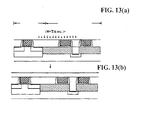
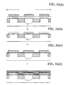
- Figures 9 through 13 show cross-sectional views [B-B' direction] of a segment of the non-volatile memory cell region of the first application embodiment of the present invention based on the damascene gate technique from which an isolating insulation film has been removed (common source region), and they show cross-sectional views of the segment of the non-volatile memory cell region from which an isolating insulation film has been removed (common source region) during the respective processes in proper order.
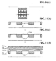
- Figures 14 through 17 show cross-sectional views [C-C' direction] of the word line direction of the non-volatile memory cell region of the first application embodiment of the present invention based on the damascene gate technique, and they show cross-sectional views of the word line direction of the non-volatile memory cell region during the respective processes in proper order. As shown in Figures 5(a), 9(a) and 14(a).
- a thermal oxide film (SiO 2 ) and an insulating film (e.g., Si 3 N 4 , ctc.) arc grown above a semiconductor substrate of a given electroconductivity type (P + ) at thicknesses of 12 nm and 200 nm, respectively, and a 300 nm channel is formed in an isolating region by means of etching by using it as a hard mask.
- An oxide film e.g., HDP, etc.
- CMP chemical mechanical polish
- an oxide film with a thickness of 10 nm is formed as the first gate insulating film (tunnel gate insulating film, TNOX) of the non-volatile memory cell based on the thermal oxidation method.
- first polycrystalline silicon film is formed over the entire plane at a thickness of 90 nm, for example, and subsequently, a 20 nm oxide film is formed above said first polycrystalline silicon film as a dummy insulating film (insulating film between wire layers). It is also possible to use a doped amorphous silicon film in place of said first polycrystalline silicon film.
- a 100 nm second polycrystalline film (dummy control gate) is formed, followed by the deposition of a 150 nm silicon nitride film (SiN film), which serves not only as an anti-reflection film but also as a stopper during an SAS (self-aligned source) etching operation, immediately above it based on a photolithographic technique. It is also possible to use a doped amorphous silicon film in place of said second polycrystalline silicon film.
- SiN film silicon nitride film
- a floating gate electrode and a dummy control gate electrode are formed patternwise in each of the peripheral transistor region and non-volatile memory cell region.
- a source-drain diffusion layer (n + diffusion layer) for the non-volatile memory cell region is formed in a self-matching fashion based on an impurity introduction technique which uses arsenic, whose electroconductivity is the opposite of that of the substrate, at an acceleration voltage of 50 keV and at a dosage of 3.0 x 10 16 dose/cm 2 .
- a 100 nm SiN film is grown based on the chemical vapor deposition method, followed by the anisotropic etching of the entire plane, as a result of which side wall insulating films are formed on the gate electrode side wall of the peripheral transistor region and the side walls of the floating gate electrode, dummy gate insulating film, and dummy control gate electrode of the non-volatile memory cell region.
- the isolating insulation film is partially removed by means of dry etching (300 nm + 10% over) by using the gate of the non-volatile memory cell region as a partial mask (SAS: Self-aligned source).
- a source-drain diffusion layer (n + diffusion layer) for the peripheral transistor region is formed in a self-matching fashion based on an impurity introduction technique which uses arsenic, whose electroconductivity is the opposite of that of the substrate, at an acceleration voltage of 60 keV and at a dosage of 3.0 x 10 15 dose/cm 2 .
- the impurity is concomitantly introduced to the segment from which the isolating insulation film has previously been removed, as a result of which a source region for the transistor and a common source wire region are formed in self-matching fashions.
- an interlayer insulating film SiO, 1,000 nm is formed.
- the dummy control gate (second polycrystalline silicon film) of each of the peripheral transistor region and non-volatile memory cell region as well as the dumnity insulating film underneath it are etched and removed over a depth of 20 nm.
- the non-volatile memory cell region (area other than the first polycrystalline silicon film-first polycrystalline silicon film gap secured for isolation purposes) is masked by using a photolithographic technique.
- the first polycrystalline silicon layer and first gate insulating film of each of the peripheral transistor region and non-volatile memory cell region are partially removed by means of an etching process (process whereby the floating gate region of the non-volatile memory cell region is induced to remain intact).
- a 1.5 nm thin SiO 2 film is formed on the channel in the aforementioned etched segment, followed by the formation of an SiON layer whose thickness is approximately 2 nm, and subsequently, a 6 nm high-permittivity film (e.g., Ta 2 O 5 ) is formed above it as a gate insulating film.
- a metal layer which may, for example, be constituted by TiN (50 nm) is formed above it.
- a layer which may, for example, be constituted by W (tungsten) is subsequently formed. As shown in Figures 8(c), 13(a) and 17(a).
- the metal layers which have been formed over the entire plane i.e., W layer and TiN layer
- a CMP chemical mechanical polish
- a 900 nm BPSG film is formed blanketwise by means of CVD (chemical vapor0 deposition), followed by the formation of a contact hole, and after an electrode wire has subsequently been formed, a non-volatile semiconductor memory device is obtained.
- CVD chemical vapor0 deposition
- NOR-type non-volatile memory has been discussed in the foregoing application embodiment ( Figures 5 through 8, Figures 9 through 13, and Figures 14 through 17), whereas in the case of an NAND-type non-volatile memory, the SAS (self-aligned source) etching process shown in Figures 9 through 13 can be dispensed with, and therefore its processes can be explained with reference to Figures 5 through 8 and Figures 9 through 13 alone.
- a metal silicide process formation of a metal reactive layer on a source-drain diffusion layer
- Figures 5 through 8, Figures 9 through 13, and Figures 14 through 17 has, furthermore, been disclosed ( Figures 5 through 8, Figures 9 through 13, and Figures 14 through 17) in the present application embodiment, but even when the present invention is applied to a non-metal silicide process, similar effects can be achieved.
- the dummy gate (second polycrystalline silicon film) is not limited to a polycrystalline silicon film so long as a proper etching selection ratio can be secured in relation to the first polycrystalline silicon film
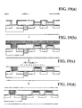
- Figures 5 through 7 and Figures 18 and 19 show cross-sectional views [D-D' direction] of an element region realm of the second application example based on a damascene gate technique, and they show cross-sectional views of the element region realm during the respective processes shown in Figures 18(b) through 19(a), which follow the process shown in Figure 7(c), in proper order.
- a thermal oxide film (SiO 2 ) and an insulating film (e.g., Si 3 N 4 , etc.) are grown above a semiconductor substrate of a given electroconductivity type (P + ) at thicknesses of 12 nm and 200 nm, respectively, and subsequently, a 300 nm channel is formed in the isolating region by using it as a hard mask.
- a 700 nm oxide film (e.g., HDP, etc.) is deposited on this channel and then planarized by means of a CMP (chemical mechanical polish) process (STI: Shallow trench insulation).
- STI chemical mechanical polish
- an oxide film whose thickness is 10 nm is formed based on the thermal oxidation method as the first gate insulating film of the non-volatile memory (tunnel gate insulating film, TNOX).
- a first polycrystalline silicon film (including DAS) whose thickness may, for example, be 90 nm is formed over the entire plane, and a 20 nm oxide film is formed above the aforementioned first polycrystalline silicon film as a dummy gate insulating film [insulating film in the PA (first wire layer)-PB (second wire layer) gap].
- a 100 nm second polycrystalline silicon film (dummy control gate which includes DAS) is formed, and a 150 nm SiN film which serves not only as an anti-reflection film but also as a stopper film during a SAS (self-aligned source) etching operation is deposited immediately above it based on a photolithographic technique.
- a floating gate electrode and a control gate electrode arc formed patternwise in each of the peripheral transistor region and non-volatile memory cell region.
- a source-drain diffusion layer (n + diffusion layer) for the non-volatile memory cell region is formed in a self-matching fashion based on an impurity introduction technique which uses arsenic, whose electroconductivity is the opposite of that of the substrate, at an acceleration voltage of 50 keV and at a dosage of 3.0 x 10 15 dose/cm 2 .
- a 100 nm SiN film is grown based on the chemical vapor deposition method, followed by the anisotropic etching (100 nm etching) of the entire plane, as a result of which side wall insulating films are formed on the gate electrode side wall of the peripheral transistor region and on the side walls of the floating gate electrode, dummy gate insulating film, and dummy control gate electrode of the non-volatile memory cell region.
- the isolating insulation film is partially removed by means of dry etching (300 nm + 10% over) by using the gate of the non-volatile memory cell region as a partial mask (SAS: Self-aligned sourcc).
- a source-drain diffusion layer (n + diffusion layer) for the peripheral transistor region is fonned in a self-matching fashion based on an impurity introduction technique which uses arsenic, whose electroconductivity is the opposite of that of the substrate, at an acceleration voltage of 60 keV and at a dosage of 3.0 x 10 15 dose/cm 2 .
- the impurity is concomitantly introduced to the segment from which the isolating insulation film has previously been removed, as a result of which a source region for the transistor and a common source wire region arc formed in self-matching fashions (formation of a common source region). As shown in Figure 6(b).
- Co (9 mn) + TiN (30 nm) is grown over the entire plane, and after a metal reactive layer (CoSi layer in this case) has been formed by means of RTA (500°C, N 2 , 30 sec.), unreacted (Co + TiN) is etched over the entire plane, followed by an additional RTA (800°C, N 2 , 30 sec.) annealing operation [formation of a metal reactive layer above the source-drain diffusion layer (silicide process)].
- an interlayer insulating film SiO, 1,000 mn
- the non-volatile memory cell region (area other than the first polycrystalline silicon film-first polycrystalline silicon film gap secured for isolating purposes) is masked by using a photolithographic technique, and the first polycrystalline silicon film and first gate insulating film of the peripheral transistor region and non-volatile memory cell region are partially removed by means of an etching process (process whereby the floating gate region of the non-volatile memory cell region is induced to remain).
- an etching process process whereby the floating gate region of the non-volatile memory cell region is induced to remain.
- a 10 nm insulating film (e.g., ONO film, etc.) is formed on the channel of the aforementioned etched segment.
- the non-volatile memory cell region alone is masked based on a photolithographic technique.
- the insulating film is removed from the peripheral transistor region by means of an etching process.
- a 1.5 nm thin SiO 2 film is formed on each of the peripheral transistor region and non-volatile memory cell region, followed by the formation of a 2 nm SiON layer, and subsequently, a 6 nm high-permittivity film (e.g., Ta 2 O 5 ) is formed above it as a gate insulating film.
- a 6 nm high-permittivity film e.g., Ta 2 O 5
- the gate insulating film of the peripheral transistor region is constituted by only one insulating film layer, whereas an insulating film laminate structure is present in the non-volatile memory cell region [it is also possible to embody a constitution wherein the peripheral transistor is constituted by a Ta 2 O 5 /non-volatile memory cell region and wherein the PA (first wire layer)-PB (second wire layer) gap insulating film is constituted by ONO in this context by removing Ta 2 O 5 while the peripheral transistor region alone is being blanketed with a resist).
- a metal layer which may, for example, be constituted by TiN (50 nm) is formed above it, followed by the formation of a W laycr (300 nm) above it.
- the metal layers which have been formed over the entire plane are polished by means of a CMP (chemical mechanical polish) process in such a way that they will remain only on the respective gate sites of the peripheral transistor region and non-volatile memory cell region.
- CMP chemical mechanical polish
- a 900 nm BPSG film is formed.
- a contact hole is subsequently formed, followed by the formation of an electrode wire, as a result of which a non-volatile semiconductor device is obtained
- cross-sectional views of the isolating region of Application Example 2 are not graphically shown because they arc identical to those of Application Example 1 shown in Figures 5 through 8, with the exception of the constitutions and thicknesses of the second gate insulating films of the peripheral transistor region and non-volatile memory cell region].
- the following procedures are carried out: After the first layer of the gate insulating film of the peripheral transistor region and the insulating film laminate structure of the non-volatile memory cell region have been formed as shown in figure 19(a) in the second application embodiment explained above, the high-permittivity film of the non-volatile memory cell region is selectively removed by means of a photolithographic technique while the peripheral transistor region alone is being masked (subsequent processes are identical to those of the second application embodiment), as a result of which the gate insulating film and the PA (first wire layer)-PB (second wire layer) gap insulating film of the peripheral transistor region differ.
- An NOR-type non-volatile memory has, furthermore, been disclosed in the second application embodiment discussed above ( Figure 19), whereas in the case of a NAND-type non-volatile memory, the SAS (self-aligned source) etching process can be dispensed with, and therefore, its processes can be explained with reference to the figures excluding Figures 9 through 13.
- a metal silicide process formation of a metal reactive layer above a source-drain diffusion layer
- bccn discussed in the aforementioned second application embodiment ( Figures 18 and 19)
- similar results can also be achieved when the same principle is applied to a non-metal silicide process.
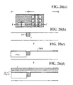
- Figures 20 through 23 show cross-sectional views [E-E' direction] of the clement region realm of the third application embodiment of the present invention based on a damascene gate technique, and the cross-sectional views of the element region realm based on the damascene gate format during the respective processes, are shown in Figures 20(a)-23(b) in proper order.
- a thermal oxide film (SiO 2 ) and an insulating film (e.g., Si 3 N 4 , etc.) are grown above a semiconductor substrate of a given electroconductivity (P [-] ) at thicknesses of 12 nm and 200 nm, respectively, and a 300 nm channel is subsequently formed on the isolating region by means of etching by using it as a hard mask.
- a 700 nm oxide film e.g., HDP, etc
- CMP chemical mechanical polish
- an oxide film whose thickness is 10 nm is formed based on the thermal oxidation method as the first gate insulating film (tunnel gate insulating film, TNOX) of the non-volatile memory cell.
- a first polycrystalline silicon film whose thickness may, for example, be 90 nm, is formed over the entire plane, and a resist for the first polycrystalline silicon film (floating gate) is subsequently etched and patterned based on a photolithographic technique, as a result of which the first polycrystalline silicon film of the non-volatile memory cell region is patterned. It is also possible to use a doped amorphous silicon film in place of said first polycrystalline silicon film.
- a 20 nm oxide film is formed above the aforementioned first polycrystalline silicon film as a gate insulating film [PA (first wire layer)-PB (second wire layer) gap insulating film].
- PA first wire layer
- PB second wire layer
- a 100 nm second polycrystalline silicon film (control gate) is formed by using a photolithographic technique. It is also possible to use a doped amorphous silicon film in place of said second polycrystalline silicon film.
- a floating gate electrode and a control gate electrode are formed patternwise in each of the peripheral transistor region and non-volatile memory cell region.
- a source-drain diffusion layer (n + diffusion layer) for the non-volatile memory cell region is formed in a self-matching fashion based on an impurity introduction technique which uses arsenic, whose electroconductivity is the opposite of that of the substrate, at an acceleration voltage of 50 keV and at a dosage of 3.0 x 10 15 dose/cm 2 .
- a 100 nm SiN film is grown based on the chemical vapor deposition method, followed by its anisotropic etching, as a result of which side wall insulating films are formed on the side wall of the gate electrode of the peripheral transistor region and on the side walls of the floating gate electrode, second gate insulating film, and control gate electrode of the non-volatile memory cell region.
- a source-drain diffusion layer (n + diffusion layer) for the non-volatile memory cell region is formed in a self-matching fashion based on an impurity introduction technique which uses arsenic, whose electroconductivity is the opposite of that of the substrate, at an acceleration voltage of 60 keV and at a dosage of 3.0 x 10 15 dose/cm 2 .
- a [Co (cobalt, 9 nm) + TiN (titanium nitride, 30 nm)] is grown over the entire plane, and after a metal reactive layer (CoSi layer in this case) has been fonned above it by means of RTA (rapid thermal annealing; 500°C, N 2 atmosphere, 30 sec.), the unreacted [Co (cobalt) + TiN (titanium nitride)] is etched back over the entire plane, and subsequently, an additional RTA (rapid thermal annealing; 800°C, N 2 atmosphere, 30 sec.) operation is carried out [formation of metal reactive layers above the source-drain region and above the gate (silicide process)].
- RTA rapid thermal annealing
- a resist pattern which blankets the non-volatile memory cell is formed based on a photolithographic technique, and the [CoSi/second polycrystalline silicon film/gate insulating film underneath the second polycrystalline silicon film/first polycrystalline silicon film/TNOX film] portion of the peripheral transistor region is removed.
- a 1.5 nm thin SiO 2 film is formed above the channel of the aforementioned etched segment, followed by the formation of a 2 nm SiON film, and a 56 nm high-permittivity film (e.g., Ta 2 O 5 ) is formed above it as a gate insulating film.
- a metal layer e.g., TiN, 50 nm
- a layer which may, for example, be constituted by W (300 nm) is formed above it.
- the metal layers (W layer and TiN layer) which have been formed over the entire plane are polished by means of a CMP (chemical mechanical polish) process in such a way that the metal gate will remain only in the gate site of the peripheral transistor region.
- CMP chemical mechanical polish
- a 900 nm BPSG (boro-phospho-silicate glass) film is formed. After a contact hole has been further formed, an electrode wire is formed, as a result of which a non-volatile semiconductor memory device is obtained.
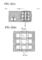
- Figures 24 and 25 show cross-sectional views [F-F' direction] of the element region realm of the fourth application embodiment of the present invention based on a damascene gate technique, and the cross-sectional views of the element region realm based on the damascene gate format during the respective processes are shown in Figures 24(a) - Figure 25(b) in proper order.
- a thermal oxide film (SiO 2 ) and an insulating film (e.g., Si 3 N 4 , etc.) are grown above a semiconductor substrate of a given electroconductivity type (P + ) at thicknesses of 12 nm and 200 nm, respectively, and a 300 nm channel is formed on the isolating region by means of etching by using it as a hard mask.
- a 700 nm oxide film is deposited on this channel, and the surface of the oxide film is polished and planarized based on the CMP (chemical mechanical polish) method.
- a shallow trench isolation (STI) is formed as a result of this flattening process.
- the use of an HDP film is especially desirable in that it is capable of achieving a high density.
- the thermal oxide film (SiO 2 ), which serves as a stopper film, and the insulating film (Si 3 N 4 ) are removed. As shown in Figure 5(b).
- an oxide film whose thickness is 10 nm is formed based on the thermal oxidation method as the first gate insulating film of the non-volatile memory (tunnel gate insulating film, TNOX).
- a first polycrystalline silicon film whose thickness may, for example, be 90 nm is formed over the entire plane, and a 20 nm oxide film is formed above the aforementioned first polycrystalline silicon film as a gate insulating film [PA (first wire layer)-PB (second wire layer) gap insulating film].
- PA first wire layer
- PB second wire layer
- a 100 nm second polycrystalline silicon film (control gate) is formed, and a 150 nm SiN (silicon nitride) film which serves not only as an anti-reflection film but also as a stopper film during an SAS (self-aligned source) etching operation is deposited immediately above it by using a photolithographic technique. It is also possible to use a doped amorphous silicon film in place of the polycrystalline silicon of said first or second polycrystalline silicon film.
- a floating gate electrode and a control gate electrode are formed patternwise in each of the peripheral transistor region and non-volatile memory cell region.
- a source-drain diffusion layer (n + diffusion layer) for the non-volatile memory cell region is formed in a self-matching fashion based on an impurity introduction technique which uses arsenic, the electroconductivity of which is the opposite of that of the substrate, at an acceleration voltage of 50 keV and at a dosage of 3.0 x 10 15 dose/cm 2 .
- a 100 nm SiN (silicon nitride) film is subsequently grown based on the chemical vapor deposition method, followed by the anisotropic etching of the entire plane (etch-back over a depth of 100 nm), as a result of which side wall insulating films are formed on the side wall of the gate electrode of the peripheral transistor region and on the side walls of the floating gate electrode, second gate insulating film, and control gate electrode of the non-volatile memory cell region.
- the isolating insulation film is partially removed by means of dry etching (300 nm + 10% over) by using the gate of the non-volatile memory cell region as a partial mask (SAS: Self-aligned source).
- a source-drain diffusion layer (n + diffusion layer) for the peripheral transistor region is formed in a self-matching fashion based on an impurity introduction technique which uses arsenic, whose electroconductivity is the opposite of that of the substrate, at an acceleration voltage of 60 keV and at a dosage of 3.0 x 10 15 dose/cm 2 .
- the impurity is concomitantly introduced to the segment from which the isolating insulation film has proviously been removed, as a result of which a source region for the transistor and a common source wire region are formed in self-matching fashion (formation of a common source region).
- an interlayer insulating film (SIO: 1,000 nm) is formed.
- the non-volatile memory cell region (area other than the first polycrystalline silicon film-first polycrystalline silicon film gap secured for isolating purposes) is masked by using a photolithographic technique, and the first polycrystalline silicon layer and first gate insulating film of each of the peripheral transistor region and non-volatile memory cell region are partially removed by means of an etching process (process whereby the element region of the non-volatile memory cell region is induced to remain).
- a thin 1.5 nm SiO 2 film is formed above the channel of the aforementioned etched segment, and after a 2 nm SION layer has subsequently been formed above it, a 6 nm high-permittivity film (e.g., Ta 2 O 5 ) is formed above it as a gate insulating film, as a result of which a third polycrystalline silicon film is formed.
- a 6 nm high-permittivity film e.g., Ta 2 O 5
- a metal layer e.g., TiN, 50 nm is formed above it.
- a layer which may, for example, be constituted by W (300 nm) is formed.
- the metal layers (W layer and TiN layer) which have been formed over the entire plane are polished by means of a CMP (chemical mechanical polish) process in such a way that only the gate sites of the peripheral transistor region and non-volatile memory cell region will remain.
- CMP chemical mechanical polish
- a 900 nm BPSG film is formed.
- a contact hole is formed, and after an electrode wire has subsequently been formed, a non-volatile semiconductor memory device is obtained [it is also possible to differentiate the control gate and floating gate materials between the non-volatile memory cell region and peripheral transistor region by removing the polycrystalline Si film of the peripheral transistor region after the formation of the third polycrystalline silicon film while the non-volatile memory cell region alone is being blanketed with a resist, by removing said resist, and by then forming a TiN [layer] (50 nm) and a W layer (300 nm)].
- the following procedures are carried out: After the third polycrystalline silicon film has been formed in Application Example 4 shown in Figure 24(b), the third polycrystalline silicon film of the peripheral transistor region alone is etched and removed by means of a photolithographic technique while the non-volatile memory cell region alone is being masked (subsequent processes are identical to those of Application Example 4), as a result of which the gate electrode structure of the peripheral transistor region and the control gate electrode structure of the non-volatile memory cell region differ.
- a NOR-type non-volatile memory has been graphically represented (Figure 24) in the present application example, whereas in the case of a NAND-type non-volatile memory, no SAS (self-aligned source) etching process is involved, and therefore its processes can be explained with reference to the figures excluding Figures 9 through 13.
- a metal silicide process (formation of a metal reactive layer above the S/D diffusion layer) has been graphically represented ( Figure 24) in the present application example, but a case of a non-metal silicide process is also within the scope of the present invention.
- Figures 27 through 33 show cross-sectional views [A-A' direction] of the element region realm of the fifth application embodiment of the present invention based on a damascene gate technique, and the cross-sectional views of the element region realm during the respective processes are thereby shown.
- the n-type transistor of the logic unit is shown on the left, whereas the cell transistor of the flash memory unit is shown on the right.
- Figure 27(b) shows cross-sectional views [A-A' direction] of the element region realm of the fifth application embodiment of the present invention based on a damascene gate technique
- the isolation region (2) is formed above the P-type semiconductor substrate (1) based on a conventionally-known LOCOS isolation method or trench isolation method. As shown in Figure 27(c).
- the silicon oxide film (3) which is to be used as a tunnel oxide film for the flash memory, is formed at a thickness of approximately 10 nm based on a conventionally-known thermal oxidation method.
- the polycrystalline silicon layer (4) which includes phosphorus at a concentration of 2 to 6 x 10 20 [atoms/cm 2 ], is subsequently formed over the entire plane at a thickness of approximately 50 nm based on a conventionally-known CVD method.
- the resist pattern (6) is formed only above the flash memory unit based on a conventionally-known photolithographic method.
- the polycrystalline silicon layer (4) of the flash memory unit not only a portion of the polycrystalline silicon layer (4) of the flash memory unit but also the polycrystalline silicon layer (4) and silicon oxide film (3) of the logic unit are removed based on a conventionally-known etching method by using the resist pattern (5) as a mask, and subsequently, the resist pattern (5) is removed.
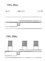
- the polycrystalline silicon layer (4) of the flash memory unit is formed in a striped fashion in a direction parallel to the isolation region (2), as the plane view of Figure 28 indicates.
- the silicon nitride film (6) is formed at a thickness of approximately 250 nm based on a conventionally-known CVD method, and subsequently, approximately 100 nm of its surface layer is polished and removed based on a conventionally-known CMP (chemical mechanical polish) method.
- CMP chemical mechanical polish
- the resist pattern (7) is formed in the shape of the gate electrode of the logic unit and flash memory unit based on a conventionally-known photolithographic method. Subsequently, the resist pattern (6) is etched based on a conventionally-known etching method by using said resist pattern (7) as a mask.
- the resist pattern (8) is formed based on a conventionally-known photolithographic method in such a way that it will blanket the logic unit.
- the polycrystalline silicon layer (4) of the flash memory unit is etched in a self-matching fashion by using the resist pattern (6), which has previously been processed into the shape of a gate electrode, as a mask based on a conventionally-known etching method.
- the polycrystalline silicon layer (4) assumes the shape of a floating gate.
- the logic unit remains unetched concomitantly in that it is being blanketed with the resist pattern (8).
- an arsenic ion is implanted into the flash memory unit at a concentration of approximately 1 x 10 15 to 1 x 10 16 [ions/cm -2 ] at 30 to 50 keV based on a conventionally-known ion implantation method while the resist pattern (8) and the prevailing state of the flash memory unit are being used as masks, as a result of which the source diffusion layer (9) and the drain diffusion layer (10) of the flash memory unit are formed.
- an ion implantation operation may be carried out after a resist pattern which covers either the source or drain has been formed. As shown in Figure 30(b).
- the resist pattern (11) is formed in such a way that it will blanket the flash memory unit, and an arsenic ion is implanted into the source-drain region of the logic unit transistor at a concentration of approximately 1 x 10 13 to 1 x 10 14 [ions/cm -2 ] at 30 to 50 keV based on a conventionally-known ion implantation method, as a result of which the LDD diffusion layer (12) is formed.
- a silicon oxide film whose thickness is approximately 100 nm is formed based on a conventionally-known CVD method, and subsequently, the side wall oxide film (13) is formed above it based on a conventionally-known etching method.
- the resist pattern (14) is formed based on a conventionally-known photolithographic method in such a way that it will blanket the flash memory unit, followed by the implantation of an arsenic ion into the source-drain region of the logic unit transistor at a concentration of approximately 1 x 10 15 to 3 x 10 15 [ions/cm -2 ] at 10 to 50 keV based on a conventionally-known ion implantation method, as a result of which the logic unit source-drain diffusion layer (15) is formed.
- a thermal treatment is performed based on a conventionally-known annealing method within a temperature range of 850 to 1,000°C for the purpose of diffusing and activating the impurity. When a high-temperature thermal treatment is thus performed preliminarily for the purpose of diffusing and activating the impurity, fears of damage to high-permittivity films and metal electrodes can be eliminated.
- the silicon oxide film (16), whose thickness is approximately 300 nm, is formed based on a conventionally-known CVD method.
- the surface of the silicon oxide film (13) is polished and flattened based on a conventionally-known CMP (chemical mechanical polish) method until the silicon nitride film (6) becomes bared.
- CMP chemical mechanical polish
- the silicon oxide film (13) is selectively removed by using a phosphoric acid solution based on a conventionally-known wet etching method, as a result of which the respective surfaces of the polycrystalline silicon layer (4) of the flash memory unit and the P-type semiconductor substrate (1) of the logic unit become bared.
- the silicon oxide film (17) whose thickness is approximately 2 nm is subsequently formed above the thus bared semiconductor substrate (1) based on a conventionally-known thermal oxidation method.
- the oxidation rate of the polycrystalline silicon is approximately twice as high as that of the semiconductor substrate (monocrystalline silicon), and therefore, a silicon oxide film (17) whose thickness is approximately 4 nm is formed above the polycrystalline silicon layer (4).
- the Ta 2 O 5 film (18), TiN film (19), and the W film (20) are formed at thicknesses of approximately 10 nm, 50 nm, and 300 nm, respectively, based on a conventionally-known CVD method.
- the silicon oxide film (17) serves as a buffer layer between the P-type semiconductor substrate (1) and the Ta 2 O 5 film (20).
- the Ta 2 O 5 film furthermore, is a high-permittivity film whose specific permittivity is approximately 5 times as high as that of the silicon oxide layer.
- the TiN film (19) serves as a barrier metal for the W film (20).
- an SiON film, ON film, or ONO film may be hereby used in place of the silicon oxide film (17).
- a nitrogen ion is implanted into the semiconductor substrate (1) and polycrystalline silicon layer (4) based on a conventionally-known ion implantation method, and subsequently, the semiconductor substrate (1) is oxidized based on a conventionally-known thermal oxidation method.
- the surface of the silicon oxide film (17) may be nitrized based on a conventionally-known thermal nitrization method upon the formation of the silicon oxide film (17).
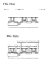
- a silicon nitride film may, for example, be formed based on a conventionally-known CVD method upon the formation of the silicon oxide film (17), followed by the oxidation of the surface of the silicon nitride film based on a conventionally-known thermal oxidation method. As shown in Figure 33(a).
- the Ta 2 O 5 film (18), TiN film (19), and the W film (20) are polished based on a conventionally-known CMP (chemical mechanical polish) method until the silicon oxide film (16) becomes bared, as a result of which the gate electrodes (21) are formed simultaneously on the logic unit and flash memory unit Since the respective gate electrode heights of the flash memory unit and logic unit can be simultaneously leveled within a single process, subsequent flattening processes become unnecessary. As shown in Figure 33(b).
- CMP chemical mechanical polish
- the contact window (23) is opened, followed by the patternwise formation of the wire layer (24).
- the interlayer insulating film (25) is formed blanketwise in such a way that it will cover the wire layer, followed by the opening of the contact window (26).
- the wire layer (27) is formed via the contact window (26).
- An upper insulating film (not shown in the figure), etc. is further formed, as a result of which a finished flash memory-logic unit heterogeneously mounted semiconductor device structure is obtained.
- an insulating film capacitance comparable to that of a 4 nm silicon oxide film can be achieved at a film thickness of 12 nm, and therefore, a structure which is more resistant to deteriorations of transistor performances attributed to leak currents than a structure wherein a silicon oxide film is used alone can be realized.
- the oxidation rate of polycrystalline silicon is approximately twice as high as that of the semiconductor substrate (1) (monocrystalline silicon), and therefore when a 2 nm silicon oxide film is formed above the semiconductor substrate (1), the thickness of the silicon oxide film (17) above the polycrystalline silicon layer (4) becomes approximately 4 nm.
- an insulating film capacitance comparable to that of a 6 nm silicon oxide film or 9 nm ON film can be realized at a film thickness of 14 nm.
- the C 1 value of the flash memory unit can be raised (i.e., higher coupling ratio) in comparison with the prior art, and accordingly the magnitude of the voltage impressed on the control gate can be lowered.
- One of the NOR types has been employed as the memory cell of the flash memory unit of the aforementioned application example, although it should be obvious that all non-volatile memories obtained by laminating floating gates and control gates can be effectively used.
- TiN has, furthermore, been used as the barrier metal for the gate electrode, but it is also possible to use silicide films or metal films which include W, Mo, Ti, Ta, etc. as well as electroconductive films whose compositions are based on their combinations.
- the gate electrode is not limited to W, and it is also possible to use metal films which include Al, Cu, etc.
- Logic unit Nch transistors alone have, furthermore, been demonstrated in the aforementioned application examples, but it should be apparent that Pch transistors are equally effective so long as the types of impurity ions, etc. are optimized.
- the silicon nitride film (6), side wall oxide film (13), and the silicon oxide film (16) of the aforementioned application example may, furthermore, be substituted with other films so long as the combinations of insulating films which are capable of selectively removing either in maskless fashion are selected.
- the resist pattern (7) alone may be selectively removed by using a hydrofluoric acid solution in Figure 1 and Figure 2.
- Either film may, furthermore, be removed selectively by means of dry etching instead of wet etching so long as a sufficient etching selection ratio can be secured.
- a simpler polymetal gate structure may, furthermore, be postulated as an advanced version of the fifth application embodiment.
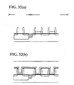
- a laminate film is formed on a gate electrode formation planned region for simulating the structure formed in the process shown in Figure 32(b), and after a coating film has been deposited on it, the surface of the gate electrode is planarized based on a CMP (chemical mechanical polish) method.
- CMP chemical mechanical polish
- the silicon oxide film (31), whose thickness is approximately 5 nm, is formed above the semiconductor substrate (1), which has been bared by a conventionally-known thermal oxidation method.
- a silicon oxide film whose thickness is approximately 10 nm is concomitantly formed above the polycrystalline silicon layer (4) in that the oxidation rate of the polycrystalline silicon is twice as high as that of the semiconductor substrate (monocrystalline silicon). It is also possible to hereby use an SiON film, ON film, or ONO film in place of the silicon oxide film (17).
- an SiON film for example, a nitrogen ion is implanted into the semiconductor substrate (1) and polycrystalline silicon layer (4) based on a conventionally-known ion implantation method, followed by the oxidation of the semiconductor substrate (1) based on a conventionally-known thermal oxidation method.
- the silicon oxide film (17) is first formed, and the surface of said silicon oxide film (17) is nitrized based on a conventionally-known thermal nitrizing method.
- a silicon nitride film is formed based on a conventionally-known CVD method upon the formation of the silicon oxide film (17), followed by the oxidation of said silicon oxide film based on a conventionally-known thermal oxidation method,
- the polycrystalline silicon film (32) whose thickness is approximately 50 nm and which includes 2 x 6 x 10 20 [atoms/cm 2 ] of phosphorus, is formed based on a conventionally-known CVD method.
- a non-doped polycrystalline film whose thickness is approximately 50 nm is formed in place of the aforementioned polycrystalline silicon film (32).
- a phosphorus ion is implanted into the aforementioned non-doped polycrystalline film at a concentration of approximately 1 x 10 15 to 5 x 10 15 [ions/cm -2 ] at 10 to 20 KeV based on a conventionally-known ion implantation method while the Pch transistor region of the logic unit is being masked by a resist pattern.
- a boron ion is implanted into the aforementioned non-doped polycrystalline film at a concentration of approximately 1 x 10 15 x 5 x 10 15 [ions/cm -2 ] at 1 to 10 KeV based on a conventionally-known ion implantation method while the areas other than the Pch transistor region of the logic unit are being masked by a resist pattern.
- a thermal treatment is performed at 850 to 1,000°C based on a conventionally-known annealing method for the purpose of diffusing and activating the impurities.
- the TiN film (33) and the W film (34), whose respective thicknesses are approximately 50 nm and 30 nm, are formed based on a conventionally-known annealing method.
- the polycrystalline silicon film (32), TiN film (33), and the W film (34) are polished based on a conventionally-known CMP (chemical mechanical polish) method until the silicon oxide film (16) becomes bared, as a result of which gate electrodes (45) with an identical height are simultaneously formed on the logic unit and the flash memory unit
- CMP chemical mechanical polish
- Figure 34 is a demonstrational diagram pertaining to the manufacturing processes of the semiconductor device of the sixth application embodiment of the present invention based on the damascene gate technique (cross-sectional view of the device), where a cross-sectional view of a single transistor of the logic device region is shown to the left of each figure, whereas a cross-sectional view of two cell transistors of the flash memory region arc shown on the right of each representation.
- the respective processes are individually shown.
- the sixth application example represents a case where an attempt is made to lower the source-drain diffusion layer resistance by integrating a salicide (self-aligned silicide) technique with the method for manufacturing the semiconductor device of the present invention.
- a thermal treatment is performed at 850 to 1,000°C based on a conventionally-known annealing method for the purpose of diffusing and activating the impurity, and the Ti (titanium) [film] (41), whose thickness ranges from 3 to 6 nm, is formed over the entire plane of the remainder of the structure based on a conventionally-known sputtering method.
- a thermal treatment is performed at 600 to 700°C based on a conventionally-known annealing method, as a result of which said Ti and the Si of the semiconductor substrate (1) become reacted, and the Ti silicide layer (TiSi 2 ) (42) is formed.
- a thermal treatment is performed at 600 to 800°C based on a conventionally-known annealing method for the purpose of lowering the resistance of the silicide layer.
- Low-resistance silicide layers arc thus formed only on the logic unit source-drain (12), flash memory unit source (9), and the drain (10).
- the Ti of the aforementioned application example may also be substituted with another metal which can form a silicide with Si (e.g., Co, Pt, Ni, etc.).
- Si e.g., Co, Pt, Ni, etc.
- an insulating film which has been temporarily formed over the entire plane is etched back until the substrate plane becomes bared in the context of forming side wall films, as a result of which the finished side wall films become completely severed from the substrate plane.
- the present invention is not limited to such isolated side wall films, and it is also possible to form a side wall film which is characterized by a tapered shape vis-à-vis the substrate plane (i.e., formation of a side wall which is not completely severed from the substrate plane) for achieving similar effects.
- a coating film which blankets the side wall film of the memory cell region and the source-drain region can be induced to remain by using as a mask a pattern which blankets said memory cell region and which possesses an opening corresponding to a peripheral region.
- CMOS Tr. and a non-volatile memory Tr. which possesses a floating gate can be mounted together in the context of manufacturing a heterogeneously memory-mounted LSI by utilizing a damascene metal gate process.
- a countermeasure against a Tr. gate depletion that would otherwise accompany an elevated peripheral transistor speed is thus provided for this non-volatile surface memory device, based on which the gate resistance gain can be inhibited at a minimum while the thickness of the gate oxide film is being reduced.
Landscapes
- Engineering & Computer Science (AREA)
- Manufacturing & Machinery (AREA)
- Semiconductor Memories (AREA)
- Non-Volatile Memory (AREA)
- Electrodes Of Semiconductors (AREA)
- Formation Of Insulating Films (AREA)
Abstract
Description
Claims (10)
- A semiconductor device, comprising:a double gate-type non-volatile memory cell which includes a first gate layer obtained by laminating a floating gate electrode, a control gate electrode of an electroconductor via an intermediate insulating film and a first gate side wall film which constitutes the side wall of said first gate layer;a peripheral transistor which includes a second gate layer of said electroconductor and a second gate side wall film which constitutes the side wall of said second gate layer;a first gate insulating film which is formed in such a way that said double gate-type non-volatile memory cell and said peripheral transistor are buried in it and whose surface has been planarized in a level fashion vis-à-vis said double gate-type non-volatile memory cell and peripheral transistor.
- The semiconductor device according to claim 1, wherein an isolating insulation film whose surface is virtually continuous and level with the surface of a semiconductor substrate is formed within said semiconductor substrate between said double gate-type non-volatile memory cell and said peripheral transistor.
- The semiconductor device according to either claims 1 or 2, wherein said intermediate insulating film and said first gate insulating film are configured beneath said first gate layer and are comprised from an identical material at an identical thickness.
- The semiconductor device according to either claims 1 or 2, wherein said intermediate insulating film and said first gate insulating film are configured beneath said first gate layer and are comprised from different materials at different thicknesses.
- The semiconductor device according to either claims 1 or 2, wherein said electroconductor is a metal.
- The semiconductor device according to either claims 1 or 2, wherein said floating gate electrode is comprised from polycrystalline silicon and wherein said control gate electrode and said second gate layer are comprised from metals.
- The semiconductor device according to either claims 1 or 2, further comprising a memory cell region which includes said double gate-type non-volatile memory cell and a peripheral transistor region which includes said peripheral transistor while they are isolated and defined by said isolating insulation film and wherein the thickness of said control gate electrode in said memory cell region exceeds the thickness of said control gate electrode above said isolating insulation film.
- A method for manufacturing a semiconductor device, said method comprising the following steps:(a) a step whereby a dummy gate pattern which consists of multiple layers and which possesses a first electroconductive layer as the lowermost layer is formed on a memory cell region and a peripheral transistor region which has been defined above a semiconductor substrate,(b) a step whereby a coating film which covers said dummy gate pattern is formed;(c) a step whereby said coating film is dry-etched in such a way that a gate side wall film will selectively remain on the side plane of said dummy gate pattern;(d) a step whereby an interlayer insulating film is formed blanketwise on the remainder of the structure formed through the preceding processes;(e) a step whereby the surface of said interlayer insulating film is etched back based on the chemical mechanical polish method until the surface of said intermediate insulating film and the surface of said dummy gate pattern become virtually continuous and flat;(f) a step whereby said dummy gate pattern is partially removed in such a way that said dummy gate pattern will be removed from said peripheral transistor region but will remain in said memory cell region and that said gate side wall film will remain in both said memory cell region and said peripheral transistor region;(g) a step whereby a second electroconductive layer is formed blanketwise on the remainder of the structure which has been formed through the preceding processes and which includes the region from which said dummy gate pattern has been removed; and(h) a step whereby the surface of said interlayer insulating film is etched back based on the chemical mechanical polish method until the surface of said interlayer insulating film and the surface of said second electroconductive layer become virtually continuous and planarized.
- The method for manufacturing a semiconductor device according to claim 8, wherein a film which possesses an upper silicon layer and a lower silicon layer which sandwich an insulating film is formed as said dummy gate pattern in said process (a), and wherein
said step (e) is implemented in such a way that said insulating film will remain and that said upper silicon layer will be removed. - The method for manufacturing a semiconductor device according to claim 8, furthering comprising the step of: a process whereby an intermediate insulating film is formed above said first electroconductive layer between said steps (e) and (f).
Applications Claiming Priority (2)
| Application Number | Priority Date | Filing Date | Title |
|---|---|---|---|
| JP2000301298 | 2000-09-29 | ||
| JP2000301298A JP4096507B2 (en) | 2000-09-29 | 2000-09-29 | Manufacturing method of semiconductor device |
Publications (2)
| Publication Number | Publication Date |
|---|---|
| EP1193762A2 true EP1193762A2 (en) | 2002-04-03 |
| EP1193762A3 EP1193762A3 (en) | 2003-02-12 |
Family
ID=18782858
Family Applications (1)
| Application Number | Title | Priority Date | Filing Date |
|---|---|---|---|
| EP01122788A Withdrawn EP1193762A3 (en) | 2000-09-29 | 2001-09-21 | Semiconductor device and its manufacturing method |
Country Status (5)
| Country | Link |
|---|---|
| US (3) | US20020043683A1 (en) |
| EP (1) | EP1193762A3 (en) |
| JP (1) | JP4096507B2 (en) |
| KR (1) | KR100805868B1 (en) |
| TW (1) | TW531898B (en) |
Cited By (3)
| Publication number | Priority date | Publication date | Assignee | Title |
|---|---|---|---|---|
| EP1759405A4 (en) * | 2004-06-25 | 2008-11-12 | Freescale Semiconductor Inc | METHOD FOR FORMING A NANOAGREGATE LOAD STORAGE DEVICE |
| CN109786230A (en) * | 2017-11-14 | 2019-05-21 | 瑞萨电子株式会社 | Semiconductor devices and its manufacturing method |
| CN109860293A (en) * | 2017-11-30 | 2019-06-07 | 台湾积体电路制造股份有限公司 | Semiconductor device and method of manufacturing the same |
Families Citing this family (68)
| Publication number | Priority date | Publication date | Assignee | Title |
|---|---|---|---|---|
| JP4774568B2 (en) * | 1999-10-01 | 2011-09-14 | ソニー株式会社 | Manufacturing method of semiconductor device |
| JP4096507B2 (en) * | 2000-09-29 | 2008-06-04 | 富士通株式会社 | Manufacturing method of semiconductor device |
| JP4439142B2 (en) | 2001-06-26 | 2010-03-24 | 株式会社東芝 | Method for manufacturing nonvolatile semiconductor memory |
| US6777725B2 (en) * | 2002-06-14 | 2004-08-17 | Ingentix Gmbh & Co. Kg | NROM memory circuit with recessed bitline |
| US6770932B2 (en) * | 2002-07-10 | 2004-08-03 | Kabushiki Kaisha Toshiba | Semiconductor memory device having a memory region and a peripheral region, and a manufacturing method thereof |
| KR100469128B1 (en) * | 2002-11-07 | 2005-01-29 | 삼성전자주식회사 | Method of forming floating gate of non-volatile memory device having self-aligned shallow trench isolation |
| KR100798268B1 (en) * | 2002-12-28 | 2008-01-24 | 동부일렉트로닉스 주식회사 | Flash memory device and manufacturing method thereof |
| KR100937651B1 (en) * | 2002-12-31 | 2010-01-19 | 동부일렉트로닉스 주식회사 | Semiconductor device and manufacturing method thereof |
| KR100511043B1 (en) * | 2003-03-07 | 2005-08-30 | 삼성전자주식회사 | Method for forming a metal silicide layer in a semiconductor device |
| JP2005026586A (en) * | 2003-07-04 | 2005-01-27 | Semiconductor Leading Edge Technologies Inc | Semiconductor device and manufacturing method thereof |
| US7002177B2 (en) * | 2003-11-05 | 2006-02-21 | Taiwan Semiconductor Manufacturing Co. Ltd. | Test region layout for shallow trench isolation |
| KR100688575B1 (en) * | 2004-10-08 | 2007-03-02 | 삼성전자주식회사 | Nonvolatile Semiconductor Memory Devices |
| TWI252512B (en) * | 2004-10-20 | 2006-04-01 | Hynix Semiconductor Inc | Semiconductor device and method of manufacturing the same |
| US7361543B2 (en) * | 2004-11-12 | 2008-04-22 | Freescale Semiconductor, Inc. | Method of forming a nanocluster charge storage device |
| KR100641993B1 (en) | 2004-12-15 | 2006-11-02 | 동부일렉트로닉스 주식회사 | Manufacturing method of CMOS image sensor having high dielectric constant insulating film |
| US8314024B2 (en) * | 2008-12-19 | 2012-11-20 | Unity Semiconductor Corporation | Device fabrication |
| KR100603694B1 (en) * | 2005-04-26 | 2006-07-20 | 매그나칩 반도체 유한회사 | Manufacturing method of semiconductor device |
| JP2007157854A (en) * | 2005-12-01 | 2007-06-21 | Toshiba Corp | Nonvolatile semiconductor memory device and manufacturing method thereof |
| KR100809328B1 (en) | 2006-07-19 | 2008-03-05 | 삼성전자주식회사 | Method for manufacturing nonvolatile memory integrated circuit device and nonvolatile memory integrated circuit device manufactured through the same |
| KR100752192B1 (en) * | 2006-09-06 | 2007-08-27 | 동부일렉트로닉스 주식회사 | Flash memory device with single poly structure and manufacturing method thereof |
| KR100843550B1 (en) | 2006-11-06 | 2008-07-04 | 삼성전자주식회사 | Nonvolatile Memory Device and Manufacturing Method Thereof |
| KR100835430B1 (en) * | 2007-05-21 | 2008-06-04 | 주식회사 동부하이텍 | Dual gate electrode formation method of semiconductor device |
| US7563675B2 (en) * | 2007-07-24 | 2009-07-21 | Taiwan Semiconductor Manufacturing Co., Ltd. | Ladder poly etching back process for word line poly planarization |
| US7745344B2 (en) * | 2007-10-29 | 2010-06-29 | Freescale Semiconductor, Inc. | Method for integrating NVM circuitry with logic circuitry |
| US7482217B1 (en) * | 2007-12-03 | 2009-01-27 | Spansion Llc | Forming metal-semiconductor films having different thicknesses within different regions of an electronic device |
| US8148249B2 (en) | 2008-09-12 | 2012-04-03 | Taiwan Semiconductor Manufacturing Company, Ltd. | Methods of fabricating high-k metal gate devices |
| US8093116B2 (en) * | 2008-10-06 | 2012-01-10 | Taiwan Semiconductor Manufacturing Company, Ltd. | Method for N/P patterning in a gate last process |
| US20100163952A1 (en) * | 2008-12-31 | 2010-07-01 | Chia-Hong Jan | Flash Cell with Integrated High-K Dielectric and Metal-Based Control Gate |
| KR20100104684A (en) * | 2009-03-18 | 2010-09-29 | 삼성전자주식회사 | Gate structure of semiconductor device and method of forming the same |
| US8399310B2 (en) | 2010-10-29 | 2013-03-19 | Freescale Semiconductor, Inc. | Non-volatile memory and logic circuit process integration |
| US8564044B2 (en) | 2011-03-31 | 2013-10-22 | Freescale Semiconductor, Inc. | Non-volatile memory and logic circuit process integration |
| US8389365B2 (en) | 2011-03-31 | 2013-03-05 | Freescale Semiconductor, Inc. | Non-volatile memory and logic circuit process integration |
| US20130049123A1 (en) * | 2011-08-23 | 2013-02-28 | Globalfoundries Inc. | Semiconductor Device with DRAM Word Lines and Gate Electrodes in Non-Memory Regions of the Device Comprised of a Metal, and Methods of Making Same |
| US9236260B2 (en) * | 2011-12-16 | 2016-01-12 | HGST Netherlands B.V. | System, method and apparatus for seedless electroplated structure on a semiconductor substrate |
| US8658497B2 (en) | 2012-01-04 | 2014-02-25 | Freescale Semiconductor, Inc. | Non-volatile memory (NVM) and logic integration |
| US8906764B2 (en) | 2012-01-04 | 2014-12-09 | Freescale Semiconductor, Inc. | Non-volatile memory (NVM) and logic integration |
| US8669158B2 (en) | 2012-01-04 | 2014-03-11 | Mark D. Hall | Non-volatile memory (NVM) and logic integration |
| US8951863B2 (en) | 2012-04-06 | 2015-02-10 | Freescale Semiconductor, Inc. | Non-volatile memory (NVM) and logic integration |
| US8722493B2 (en) | 2012-04-09 | 2014-05-13 | Freescale Semiconductor, Inc. | Logic transistor and non-volatile memory cell integration |
| US9087913B2 (en) | 2012-04-09 | 2015-07-21 | Freescale Semiconductor, Inc. | Integration technique using thermal oxide select gate dielectric for select gate and apartial replacement gate for logic |
| US8728886B2 (en) * | 2012-06-08 | 2014-05-20 | Freescale Semiconductor, Inc. | Integrating formation of a replacement gate transistor and a non-volatile memory cell using a high-k dielectric |
| US8574987B1 (en) | 2012-06-08 | 2013-11-05 | Freescale Semiconductor, Inc. | Integrating formation of a replacement gate transistor and a non-volatile memory cell using an interlayer dielectric |
| US9111865B2 (en) | 2012-10-26 | 2015-08-18 | Freescale Semiconductor, Inc. | Method of making a logic transistor and a non-volatile memory (NVM) cell |
| CN103854985B (en) * | 2012-12-03 | 2016-06-29 | 中国科学院微电子研究所 | A method for manufacturing a dummy gate of the gate-last process and a dummy gate of the gate-last process |
| JP6026914B2 (en) * | 2013-02-12 | 2016-11-16 | ルネサスエレクトロニクス株式会社 | Manufacturing method of semiconductor device |
| JP2014165457A (en) * | 2013-02-27 | 2014-09-08 | Toshiba Corp | Manufacturing method of nonvolatile semiconductor memory device |
| US8716089B1 (en) | 2013-03-08 | 2014-05-06 | Freescale Semiconductor, Inc. | Integrating formation of a replacement gate transistor and a non-volatile memory cell having thin film storage |
| US8741719B1 (en) | 2013-03-08 | 2014-06-03 | Freescale Semiconductor, Inc. | Integrating formation of a logic transistor and a non-volatile memory cell using a partial replacement gate technique |
| US9006093B2 (en) | 2013-06-27 | 2015-04-14 | Freescale Semiconductor, Inc. | Non-volatile memory (NVM) and high voltage transistor integration |
| US8871598B1 (en) | 2013-07-31 | 2014-10-28 | Freescale Semiconductor, Inc. | Non-volatile memory (NVM) and high-k and metal gate integration using gate-first methodology |
| US9129996B2 (en) | 2013-07-31 | 2015-09-08 | Freescale Semiconductor, Inc. | Non-volatile memory (NVM) cell and high-K and metal gate transistor integration |
| US8877585B1 (en) | 2013-08-16 | 2014-11-04 | Freescale Semiconductor, Inc. | Non-volatile memory (NVM) cell, high voltage transistor, and high-K and metal gate transistor integration |
| US9082837B2 (en) | 2013-08-08 | 2015-07-14 | Freescale Semiconductor, Inc. | Nonvolatile memory bitcell with inlaid high k metal select gate |
| US9082650B2 (en) * | 2013-08-21 | 2015-07-14 | Freescale Semiconductor, Inc. | Integrated split gate non-volatile memory cell and logic structure |
| US9252246B2 (en) | 2013-08-21 | 2016-02-02 | Freescale Semiconductor, Inc. | Integrated split gate non-volatile memory cell and logic device |
| US9275864B2 (en) | 2013-08-22 | 2016-03-01 | Freescale Semiconductor,Inc. | Method to form a polysilicon nanocrystal thin film storage bitcell within a high k metal gate platform technology using a gate last process to form transistor gates |
| US8932925B1 (en) | 2013-08-22 | 2015-01-13 | Freescale Semiconductor, Inc. | Split-gate non-volatile memory (NVM) cell and device structure integration |
| US8883624B1 (en) * | 2013-09-27 | 2014-11-11 | Cypress Semiconductor Corporation | Integration of a memory transistor into high-K, metal gate CMOS process flow |
| US8901632B1 (en) | 2013-09-30 | 2014-12-02 | Freescale Semiconductor, Inc. | Non-volatile memory (NVM) and high-K and metal gate integration using gate-last methodology |
| US9129855B2 (en) | 2013-09-30 | 2015-09-08 | Freescale Semiconductor, Inc. | Non-volatile memory (NVM) and high-k and metal gate integration using gate-first methodology |
| US9136129B2 (en) | 2013-09-30 | 2015-09-15 | Freescale Semiconductor, Inc. | Non-volatile memory (NVM) and high-k and metal gate integration using gate-last methodology |
| US9231077B2 (en) | 2014-03-03 | 2016-01-05 | Freescale Semiconductor, Inc. | Method of making a logic transistor and non-volatile memory (NVM) cell |
| US9252152B2 (en) | 2014-03-28 | 2016-02-02 | Freescale Semiconductor, Inc. | Method for forming a split-gate device |
| US9472418B2 (en) | 2014-03-28 | 2016-10-18 | Freescale Semiconductor, Inc. | Method for forming a split-gate device |
| US9112056B1 (en) | 2014-03-28 | 2015-08-18 | Freescale Semiconductor, Inc. | Method for forming a split-gate device |
| US9379222B2 (en) | 2014-05-30 | 2016-06-28 | Freescale Semiconductor, Inc. | Method of making a split gate non-volatile memory (NVM) cell |
| US9343314B2 (en) | 2014-05-30 | 2016-05-17 | Freescale Semiconductor, Inc. | Split gate nanocrystal memory integration |
| US9257445B2 (en) | 2014-05-30 | 2016-02-09 | Freescale Semiconductor, Inc. | Method of making a split gate non-volatile memory (NVM) cell and a logic transistor |
Family Cites Families (20)
| Publication number | Priority date | Publication date | Assignee | Title |
|---|---|---|---|---|
| JP2664685B2 (en) * | 1987-07-31 | 1997-10-15 | 株式会社東芝 | Method for manufacturing semiconductor device |
| DE69322928T2 (en) * | 1992-10-27 | 1999-07-29 | Nec Corp., Tokio/Tokyo | Method of manufacturing a non-volatile semiconductor memory device |
| JPH09205154A (en) * | 1996-01-25 | 1997-08-05 | Mitsubishi Electric Corp | Semiconductor device and manufacturing method thereof |
| KR980012447A (en) * | 1996-07-19 | 1998-04-30 | 김광호 | Method for forming a gate electrode of a nonvolatile semiconductor device |
| JP3107199B2 (en) * | 1996-08-29 | 2000-11-06 | 日本電気株式会社 | Manufacturing method of nonvolatile semiconductor memory device |
| JPH10189966A (en) * | 1996-12-26 | 1998-07-21 | Toshiba Corp | Semiconductor device and manufacturing method thereof |
| JPH10303401A (en) * | 1997-02-25 | 1998-11-13 | Mitsubishi Electric Corp | Semiconductor device and manufacturing method thereof |
| JPH1117035A (en) * | 1997-06-24 | 1999-01-22 | Mitsubishi Electric Corp | Nonvolatile semiconductor memory device and method of manufacturing the same |
| JP3264241B2 (en) * | 1998-02-10 | 2002-03-11 | 日本電気株式会社 | Method for manufacturing semiconductor device |
| JP2000022008A (en) * | 1998-07-01 | 2000-01-21 | Mitsubishi Electric Corp | Nonvolatile semiconductor memory device and method of manufacturing the same |
| EP0975022A1 (en) * | 1998-07-22 | 2000-01-26 | STMicroelectronics S.r.l. | Method for manufacturing electronic devices comprising non-volatile memory cells and LV transistors, with salicided junctions |
| TW449919B (en) * | 1998-12-18 | 2001-08-11 | Koninkl Philips Electronics Nv | A method of manufacturing a semiconductor device |
| US6259126B1 (en) * | 1999-11-23 | 2001-07-10 | International Business Machines Corporation | Low cost mixed memory integration with FERAM |
| KR100350056B1 (en) * | 2000-03-09 | 2002-08-24 | 삼성전자 주식회사 | Method of forming a self-aligned contact pad in a damascene gate process |
| TW466606B (en) * | 2000-04-20 | 2001-12-01 | United Microelectronics Corp | Manufacturing method for dual metal gate electrode |
| JP4096507B2 (en) * | 2000-09-29 | 2008-06-04 | 富士通株式会社 | Manufacturing method of semiconductor device |
| JP2003243618A (en) * | 2002-02-20 | 2003-08-29 | Seiko Epson Corp | Method for manufacturing semiconductor device |
| KR100481863B1 (en) * | 2002-10-11 | 2005-04-11 | 삼성전자주식회사 | Semiconductor device and method of forming the same |
| JP2005026589A (en) * | 2003-07-04 | 2005-01-27 | Toshiba Corp | Semiconductor memory device and manufacturing method thereof |
| US7271083B2 (en) * | 2004-07-22 | 2007-09-18 | Taiwan Semiconductor Manufacturing Company, Ltd. | One-transistor random access memory technology compatible with metal gate process |
-
2000
- 2000-09-29 JP JP2000301298A patent/JP4096507B2/en not_active Expired - Fee Related
-
2001
- 2001-09-21 EP EP01122788A patent/EP1193762A3/en not_active Withdrawn
- 2001-09-28 US US09/964,592 patent/US20020043683A1/en not_active Abandoned
- 2001-09-28 TW TW090124095A patent/TW531898B/en not_active IP Right Cessation
- 2001-09-29 KR KR1020010060902A patent/KR100805868B1/en not_active Expired - Fee Related
-
2003
- 2003-04-28 US US10/423,963 patent/US20040075133A1/en not_active Abandoned
-
2006
- 2006-11-21 US US11/602,246 patent/US7476582B2/en not_active Expired - Fee Related
Cited By (4)
| Publication number | Priority date | Publication date | Assignee | Title |
|---|---|---|---|---|
| EP1759405A4 (en) * | 2004-06-25 | 2008-11-12 | Freescale Semiconductor Inc | METHOD FOR FORMING A NANOAGREGATE LOAD STORAGE DEVICE |
| CN109786230A (en) * | 2017-11-14 | 2019-05-21 | 瑞萨电子株式会社 | Semiconductor devices and its manufacturing method |
| CN109786230B (en) * | 2017-11-14 | 2024-02-09 | 瑞萨电子株式会社 | Semiconductor device and method for manufacturing the same |
| CN109860293A (en) * | 2017-11-30 | 2019-06-07 | 台湾积体电路制造股份有限公司 | Semiconductor device and method of manufacturing the same |
Also Published As
| Publication number | Publication date |
|---|---|
| US20070066004A1 (en) | 2007-03-22 |
| KR20020025839A (en) | 2002-04-04 |
| US20020043683A1 (en) | 2002-04-18 |
| KR100805868B1 (en) | 2008-02-20 |
| JP4096507B2 (en) | 2008-06-04 |
| TW531898B (en) | 2003-05-11 |
| US7476582B2 (en) | 2009-01-13 |
| EP1193762A3 (en) | 2003-02-12 |
| US20040075133A1 (en) | 2004-04-22 |
| JP2002110824A (en) | 2002-04-12 |
Similar Documents
| Publication | Publication Date | Title |
|---|---|---|
| US7476582B2 (en) | Semiconductor device and its manufacturing method | |
| US6777725B2 (en) | NROM memory circuit with recessed bitline | |
| EP1057218B1 (en) | A method of manufacturing a semiconductor device | |
| US8940603B2 (en) | Method of making semiconductor device | |
| US6689658B2 (en) | Methods of fabricating a stack-gate flash memory array | |
| KR100450802B1 (en) | Double gate trench transistor | |
| JP4151992B2 (en) | Semiconductor integrated circuit device | |
| US5811853A (en) | Single-side oxide sealed salicide for EPROMS | |
| US6989560B2 (en) | Semiconductor device and method of fabricating the same | |
| US5804472A (en) | Method of making spacer-type thin-film polysilicon transistor for low-power memory devices | |
| JP2001044391A (en) | Semiconductor memory device and manufacturing method thereof | |
| IE970456A1 (en) | Eeprom having coplanar on-insulator fet and control gate | |
| JP2003501806A (en) | Single polysilicon flash EEPROM and manufacturing method | |
| US7919367B2 (en) | Method to increase charge retention of non-volatile memory manufactured in a single-gate logic process | |
| US20090085213A1 (en) | Semiconductor device and method of fabrication | |
| JP2004519094A (en) | Self-aligned nonvolatile memory cell | |
| US6849490B2 (en) | Semiconductor device having a memory cell region and a peripheral circuit region and method of manufacturing thereof | |
| US6448163B1 (en) | Method for fabricating T-shaped transistor gate | |
| TWI276217B (en) | Non-volatile semiconductor memory and process of fabricating the same | |
| JP2005191489A (en) | Semiconductor memory device and manufacturing method thereof | |
| JPH10223781A (en) | Semiconductor device and manufacturing method thereof | |
| JP4266089B2 (en) | Manufacturing method of semiconductor memory device | |
| US6682978B1 (en) | Integrated circuit having increased gate coupling capacitance | |
| US7470614B1 (en) | Methods for fabricating semiconductor devices and contacts to semiconductor devices | |
| JP2003229499A (en) | Semiconductor memory device and method of manufacturing the same |
Legal Events
| Date | Code | Title | Description |
|---|---|---|---|
| PUAI | Public reference made under article 153(3) epc to a published international application that has entered the european phase |
Free format text: ORIGINAL CODE: 0009012 |
|
| AK | Designated contracting states |
Kind code of ref document: A2 Designated state(s): AT BE CH CY DE DK ES FI FR GB GR IE IT LI LU MC NL PT SE TR |
|
| AX | Request for extension of the european patent |
Free format text: AL;LT;LV;MK;RO;SI |
|
| PUAL | Search report despatched |
Free format text: ORIGINAL CODE: 0009013 |
|
| AK | Designated contracting states |
Designated state(s): AT BE CH CY DE DK ES FI FR GB GR IE IT LI LU MC NL PT SE TR |
|
| AX | Request for extension of the european patent |
Extension state: AL LT LV MK RO SI |
|
| 17P | Request for examination filed |
Effective date: 20030715 |
|
| AKX | Designation fees paid |
Designated state(s): DE FR IT |
|
| 17Q | First examination report despatched |
Effective date: 20080314 |
|
| RAP1 | Party data changed (applicant data changed or rights of an application transferred) |
Owner name: FUJITSU MICROELECTRONICS LIMITED |
|
| RAP1 | Party data changed (applicant data changed or rights of an application transferred) |
Owner name: FUJITSU SEMICONDUCTOR LIMITED |
|
| STAA | Information on the status of an ep patent application or granted ep patent |
Free format text: STATUS: THE APPLICATION IS DEEMED TO BE WITHDRAWN |
|
| 18D | Application deemed to be withdrawn |
Effective date: 20110329 |