EP1192726B1 - Structure of a radio-frequency front end - Google Patents
Structure of a radio-frequency front end Download PDFInfo
- Publication number
- EP1192726B1 EP1192726B1 EP00949504A EP00949504A EP1192726B1 EP 1192726 B1 EP1192726 B1 EP 1192726B1 EP 00949504 A EP00949504 A EP 00949504A EP 00949504 A EP00949504 A EP 00949504A EP 1192726 B1 EP1192726 B1 EP 1192726B1
- Authority
- EP
- European Patent Office
- Prior art keywords
- circuit board
- antenna
- filter
- amplifier
- protective frame
- Prior art date
- Legal status (The legal status is an assumption and is not a legal conclusion. Google has not performed a legal analysis and makes no representation as to the accuracy of the status listed.)
- Expired - Lifetime
Links
Images


Classifications
-
- H—ELECTRICITY
- H01—ELECTRIC ELEMENTS
- H01Q—ANTENNAS, i.e. RADIO AERIALS
- H01Q9/00—Electrically-short antennas having dimensions not more than twice the operating wavelength and consisting of conductive active radiating elements
- H01Q9/04—Resonant antennas
- H01Q9/0407—Substantially flat resonant element parallel to ground plane, e.g. patch antenna
-
- H—ELECTRICITY
- H01—ELECTRIC ELEMENTS
- H01Q—ANTENNAS, i.e. RADIO AERIALS
- H01Q1/00—Details of, or arrangements associated with, antennas
- H01Q1/12—Supports; Mounting means
- H01Q1/22—Supports; Mounting means by structural association with other equipment or articles
- H01Q1/24—Supports; Mounting means by structural association with other equipment or articles with receiving set
- H01Q1/241—Supports; Mounting means by structural association with other equipment or articles with receiving set used in mobile communications, e.g. GSM
- H01Q1/242—Supports; Mounting means by structural association with other equipment or articles with receiving set used in mobile communications, e.g. GSM specially adapted for hand-held use
- H01Q1/243—Supports; Mounting means by structural association with other equipment or articles with receiving set used in mobile communications, e.g. GSM specially adapted for hand-held use with built-in antennas
-
- H—ELECTRICITY
- H01—ELECTRIC ELEMENTS
- H01Q—ANTENNAS, i.e. RADIO AERIALS
- H01Q1/00—Details of, or arrangements associated with, antennas
- H01Q1/36—Structural form of radiating elements, e.g. cone, spiral, umbrella; Particular materials used therewith
- H01Q1/38—Structural form of radiating elements, e.g. cone, spiral, umbrella; Particular materials used therewith formed by a conductive layer on an insulating support
-
- H—ELECTRICITY
- H01—ELECTRIC ELEMENTS
- H01Q—ANTENNAS, i.e. RADIO AERIALS
- H01Q23/00—Antennas with active circuits or circuit elements integrated within them or attached to them
-
- H—ELECTRICITY
- H04—ELECTRIC COMMUNICATION TECHNIQUE
- H04B—TRANSMISSION
- H04B1/00—Details of transmission systems, not covered by a single one of groups H04B3/00 - H04B13/00; Details of transmission systems not characterised by the medium used for transmission
- H04B1/06—Receivers
- H04B1/16—Circuits
- H04B1/26—Circuits for superheterodyne receivers
- H04B1/28—Circuits for superheterodyne receivers the receiver comprising at least one semiconductor device having three or more electrodes
-
- H—ELECTRICITY
- H03—ELECTRONIC CIRCUITRY
- H03D—DEMODULATION OR TRANSFERENCE OF MODULATION FROM ONE CARRIER TO ANOTHER
- H03D7/00—Transference of modulation from one carrier to another, e.g. frequency-changing
- H03D7/16—Multiple-frequency-changing
- H03D7/165—Multiple-frequency-changing at least two frequency changers being located in different paths, e.g. in two paths with carriers in quadrature
Definitions
- the invention relates to an integrated structure of a radio-frequency front end in a communications apparatus.
- the front end comprises at least an antenna as well as a radio-frequency amplifier and filter both in the transmit and receive branch.
- filters are needed in the radio-frequency part of a bi-directional radio apparatus such as a mobile station. Extra frequency components produced by a mixer as well as extra frequency components produced by a power amplifier have to be removed in the transmit branch. In the receive branch, filters are needed in order to achieve basic selectivity, protect a low-noise pre-amplifier, and to attenuate noise generated by the transmitter on the receive band. In the case of different transmit and receive frequencies a duplex filter is generally used to mutually separate the different directions of transmission. An antenna switch is used in systems in which the transmit and receive frequencies are the same, and in systems where transmission and reception take place both at different frequencies and at different moments of time. Other functional units in a radio-frequency front end include the aforementioned amplifiers, a directional coupler for measuring the transmission power for power control, and mixers.
- RF circuit input and output impedances are often different: for example, the optimum input impedance level of a LNA is about 100 to 200 ⁇ . If the amplifier has this input impedance, the matching to the standard impedance of the preceding circuit requires a separate matching circuit. This will increase both the size and cost of the radio apparatus. Moreover, the matching circuit causes additional losses on the signal on the transmission path, which, in turn, means a shorter talk time, among other things.
- Radios according to the prior art usually comprise at least one integrated component and discrete filters connected to it/them.
- Patent document WO 93/14573 discloses a solution applicable to time division multiple access wherein all active components of the transceiver are integrated into a single circuit.
- a disadvantage of this solution is that there are matching problems between the integrated circuit and the filters external to it.
- the integrated circuit does not contain a directional coupler.
- An external directional coupler built into a printed circuit board is susceptible to electric disturbances, requires a considerable amount of space on the printed circuit board and, in addition, causes an extra loss of at least 0.5 dB in the transmitter chain, which has a direct impact on the current consumption of the communications apparatus.
- U.S. Patent No. 5,432,489 discloses a solution that uses transmission lines belonging to circuits of the transmitter branch bandpass filter or to matching circuit, as part of a directional coupler. This way, the directional coupler can be moved from the printed circuit board onto a low-loss substrate and inside the protective housing of the high-frequency filter.
- the advantage of the solution is that it saves space and reduces susceptibility to interference as well as the transmission loss caused by the directional coupler, but the disadvantage is that in other respects the integration problems remain.
- An advantage of the structure according to Fig. 1 is that the number of structural elements needed for matching at the input of amplifier LNA and output of amplifier PA is smaller as there is no need to provide matching to the 50 ⁇ impedance level. Additional advantages include a reduction of parasitic effects, reduction of the number of components inserted onto the printed circuit board of the communications apparatus and reduction of the area needed on the circuit board.
- a drawback of the structure is that the transmit branch bandpass filter 20 and receive branch bandpass filter 30, shown in Fig. 1a, are still separate units on the circuit board. The antenna, too, is a discrete component.
- An object of the invention is to reduce the above described disadvantages of the prior art.
- the structure according to the invention is characterized by what is expressed in the independent claim. Preferred embodiments of the invention are disclosed in the other claims.
- the basic idea of the invention is as follows:
- the antenna of the communications apparatus is constructed on a printed circuit board.
- a second printed circuit board is attached by means of a rigid protective frame, which second circuit board includes the other parts of the radio-frequency front end. Between the parts impedance levels are used that are appropriate from the electrical operation perspective. All said parts together form a solid component to be located inside the housing of the communications apparatus.
- Fig. 2 shows a block diagram of a possible radio-frequency front end of a communications apparatus.
- the front end 200 comprises an antenna 210, duplex filter 220, low-noise amplifier 230, bandpass filters 241 and 242, and a power amplifier 250.
- the antenna is connected to a bi-directional antenna port in the duplex filter 220.
- the receive port of the duplex filter is connected to the input of the amplifier 230, and the output of the amplifier 230 is connected to the input of the bandpass filter 241.
- the output of the filter 241 is connected to the receive branch mixer, and the input of the filter 242 is connected to the transmit branch mixer.
- the output of the filter 242 is connected to the input of the amplifier 250, and the output of the amplifier 250 is connected to the transmit port of the duplex filter 220.
- Fig. 3a shows an example of an antenna structure according to the invention. What is essential is that the antenna as a component is board-like.
- Fig. 3a shows an antenna circuit board 310 which has on its lower surface, or second surface, which is not visible in Fig. 3a, a ground plane 311 which covers substantially the whole area of the surface.
- Conductive areas 312 and 313 are planar, and if, in addition to having a common feed, they are shorted to ground, they form a dual-frequency planar inverted-F antenna (PIFA).
- Conductive patch 314 comprises a meander-patterned conductor. It can be made to radiate at either of the PIFA frequency ranges or at some third frequency range.
- the board 310 is drawn in Fig. 3a considerably larger than its real size.
- Fig. 3b illustrates a way of assembling the other functional units of the RF front end.
- a board-like piece 321 which may be a printed circuit board.
- modules 220, 230, 240 and 250 are placed on the board 321.
- the reference numerals correspond to those of Fig. 2.
- Module 220 comprises a duplex filter
- module 230 a low-noise amplifier LNA
- module 250 comprises a power amplifier PA.
- the filters are realized using coaxial resonators.
- Fig. 3b shows a pin-like conductor 323 the function of which is to provide a connection between the board 321 and antenna board 310.
- the conductor 323 is by its lower end connected to the filter 220 through a conductive strip 322.
- the other connections on the board 321 are not shown.
- the lower surface of the board 321, which is not visible in Fig. 3b, is conductive.
- the board 321 and the modules on it are drawn considerably larger than they are in real life.
- Fig. 4 shows an example of a front end assembled into a single component.
- the component 400 comprises an antenna circuit board 310, module assembly 320 and a rigid mechanical frame 410.
- the frame 410 supports both the antenna board and board 321.
- a protective housing for the filters and amplifiers is produced.
- Fig. 4 shows a conductor 420 extending downward, which is one conductor between the component 400 and the rest of the communications apparatus.
- the parts shown in Fig. 4 are mechanically strong and firmly attached to each other so that the component 400 formed is compact. In real life it is smaller than in the drawing.
- the invention does not limit the number or size of the elements in the antenna board. Neither does the invention limit the number or nature or internal realization of the RF units in the front end.
- the present invention is not limited to any particular application, too. It can be used in transceivers in various applications and at different frequencies and with different multiple access methods, advantageously at radio frequencies such as UHF and VHF.
- the arrangement according to the invention can be used in subscriber apparatus of a system based on digital time division multiple access (TDMA/FDMA, TDMA/FDD, or TDMA/TDD) that have a separate or integrated antenna, in car phones and in hand phones.
- TDMA/FDMA digital time division multiple access
- TDMA/FDD time division multiple access
- TDMA/TDD time division multiple access
Landscapes
- Engineering & Computer Science (AREA)
- Computer Networks & Wireless Communication (AREA)
- Signal Processing (AREA)
- Transceivers (AREA)
Description
- The invention relates to an integrated structure of a radio-frequency front end in a communications apparatus. The front end comprises at least an antenna as well as a radio-frequency amplifier and filter both in the transmit and receive branch.
- Several filters are needed in the radio-frequency part of a bi-directional radio apparatus such as a mobile station. Extra frequency components produced by a mixer as well as extra frequency components produced by a power amplifier have to be removed in the transmit branch. In the receive branch, filters are needed in order to achieve basic selectivity, protect a low-noise pre-amplifier, and to attenuate noise generated by the transmitter on the receive band. In the case of different transmit and receive frequencies a duplex filter is generally used to mutually separate the different directions of transmission. An antenna switch is used in systems in which the transmit and receive frequencies are the same, and in systems where transmission and reception take place both at different frequencies and at different moments of time. Other functional units in a radio-frequency front end include the aforementioned amplifiers, a directional coupler for measuring the transmission power for power control, and mixers.
- Integration of successive radio-frequency units is difficult mainly because of the relatively large size of the filters. If, for example, an antenna switch, a low-noise amplifier (LNA) and a filter between them are integrated on one chip, the large size of the filter calls for relatively large connection strips that produce electrical stray quantities and inductive couplings which degrade the selectivity of the filter. Complete integration of a filter between active RF units with other units is therefore impractical.
- Another thing that makes integration difficult is the fact that commercial components usually have input and output impedances of 50 Ω in order to make modular design easier. However, advantageous values for RF circuit input and output impedances are often different: for example, the optimum input impedance level of a LNA is about 100 to 200 Ω. If the amplifier has this input impedance, the matching to the standard impedance of the preceding circuit requires a separate matching circuit. This will increase both the size and cost of the radio apparatus. Moreover, the matching circuit causes additional losses on the signal on the transmission path, which, in turn, means a shorter talk time, among other things.
- From the prior art it is known numerous structures aimed at achieving as high degree of integration of RF circuits as possible. Radios according to the prior art usually comprise at least one integrated component and discrete filters connected to it/them.
- Patent document
WO 93/14573 - From
U.S. Patent No. 4,792,939 a solution is known in which a duplexer, transmitter and receiver are integrated on one chip. In that solution the duplexer, a bandpass filter and a mixer are implemented using surface acoustic wave (SAW) technology. A drawback of the arrangement is that the matching circuits required by the SAW circuits are so large and the SAW circuits themselves are so lossy and have such a poor power capacity compared to the transmission power that application of the solution in a modem mobile phone is impossible. -
U.S. Patent No. 5,432,489 discloses a solution that uses transmission lines belonging to circuits of the transmitter branch bandpass filter or to matching circuit, as part of a directional coupler. This way, the directional coupler can be moved from the printed circuit board onto a low-loss substrate and inside the protective housing of the high-frequency filter. The advantage of the solution is that it saves space and reduces susceptibility to interference as well as the transmission loss caused by the directional coupler, but the disadvantage is that in other respects the integration problems remain. - From
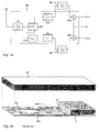
U.S. Patent No. 5,903,820 it is known a solution in which an antenna filter AFI, antenna switch ASW, directional coupler DCO, low-noise amplifier LNA, mixers MIX, and a power amplifier PA are integrated into one entity. This entity forms one component on the printed circuit board of a mobile station. Fig. 1 a shows a block diagram ofsaid entity 10, which is to be integrated. Fig. 1b shows an example of the practical implementation of thecircuit 10. In the example, all parts are assembled onto one and the same low-loss substrate S. The most space-consuming parts are thecoaxial resonators - An advantage of the structure according to Fig. 1 is that the number of structural elements needed for matching at the input of amplifier LNA and output of amplifier PA is smaller as there is no need to provide matching to the 50 Ω impedance level. Additional advantages include a reduction of parasitic effects, reduction of the number of components inserted onto the printed circuit board of the communications apparatus and reduction of the area needed on the circuit board. A drawback of the structure is that the transmit
branch bandpass filter 20 and receivebranch bandpass filter 30, shown in Fig. 1a, are still separate units on the circuit board. The antenna, too, is a discrete component. - An object of the invention is to reduce the above described disadvantages of the prior art. The structure according to the invention is characterized by what is expressed in the independent claim. Preferred embodiments of the invention are disclosed in the other claims.
- The basic idea of the invention is as follows: The antenna of the communications apparatus is constructed on a printed circuit board. To the antenna board, on its ground plane side, a second printed circuit board is attached by means of a rigid protective frame, which second circuit board includes the other parts of the radio-frequency front end. Between the parts impedance levels are used that are appropriate from the electrical operation perspective. All said parts together form a solid component to be located inside the housing of the communications apparatus.
- An advantage of the invention is that the number of structural elements needed for matching between the RF parts is smaller than in prior-art structures. Another advantage of the invention is that it makes possible a greater sensitivity of receiver than prior art structures. The noise figure and the sensitivity of the receiver branch can be improved by means of internal optimization, for example. A further advantage of the invention is that it makes possible lower losses in the transmitter than prior art structures. For example, changing the input impedance of the power amplifier PA from 50 Ω to 2 Ω makes the design of the power amplifier considerably easier, at the same improving the efficiency of the power amplifier. Still another advantage of the invention is that it provides a single component that comprises the whole radio-frequency front end including the antenna. This leads to smaller communications apparatus and simplification of design.
- The invention will now be described in detail. Reference will be made to the accompanying drawing wherein
- Fig. 1a
- shows in the form of block diagram an example of the front end of a communications apparatus,
- Fig. 1b
- shows an example of the practical implementation of the prior-art front end according to Fig. 1a,
- Fig. 2
- shows in the form of block diagram a second example of the front end of a communications apparatus,
- Fig. 3a
- shows an example of an antenna board according to the invention,
- Fig. 3b
- shows an example of a placement according to the invention of functional modules, and
- Fig. 4
- shows in the form of component an example of a front end according to the invention.
- Figs. 1a and 1b were already discussed in connection with the description of the prior art.
- Fig. 2 shows a block diagram of a possible radio-frequency front end of a communications apparatus. The
front end 200 comprises anantenna 210,duplex filter 220, low-noise amplifier 230,bandpass filters power amplifier 250. The antenna is connected to a bi-directional antenna port in theduplex filter 220. The receive port of the duplex filter is connected to the input of theamplifier 230, and the output of theamplifier 230 is connected to the input of thebandpass filter 241. The output of thefilter 241 is connected to the receive branch mixer, and the input of thefilter 242 is connected to the transmit branch mixer. The output of thefilter 242 is connected to the input of theamplifier 250, and the output of theamplifier 250 is connected to the transmit port of theduplex filter 220. - Next it will be described how a
front end 200 according to Fig. 2 is integrated into a single component in accordance with the invention. - Fig. 3a shows an example of an antenna structure according to the invention. What is essential is that the antenna as a component is board-like. Fig. 3a shows an
antenna circuit board 310 which has on its lower surface, or second surface, which is not visible in Fig. 3a, aground plane 311 which covers substantially the whole area of the surface. On the upper surface, or first surface, of thecircuit board 310 there are in this example three radiating elements:conductive areas Conductive areas Conductive patch 314 comprises a meander-patterned conductor. It can be made to radiate at either of the PIFA frequency ranges or at some third frequency range. Theboard 310 is drawn in Fig. 3a considerably larger than its real size. - Fig. 3b illustrates a way of assembling the other functional units of the RF front end. Shown in Fig. 3b is a board-
like piece 321 which may be a printed circuit board. Fourmodules board 321. The reference numerals correspond to those of Fig. 2.Module 220 comprises a duplex filter, module 230 a low-noise amplifier LNA,module 240bandpass filters module 250 comprises a power amplifier PA. In this example the filters are realized using coaxial resonators. In the figure is pointed to oneresonator 325. Fig. 3b shows a pin-like conductor 323 the function of which is to provide a connection between theboard 321 andantenna board 310. Theconductor 323 is by its lower end connected to thefilter 220 through aconductive strip 322. The other connections on theboard 321 are not shown. The lower surface of theboard 321, which is not visible in Fig. 3b, is conductive. Theboard 321 and the modules on it are drawn considerably larger than they are in real life. - Fig. 4 shows an example of a front end assembled into a single component. The
component 400 comprises anantenna circuit board 310,module assembly 320 and a rigidmechanical frame 410. Theframe 410 supports both the antenna board andboard 321. Thereby is produced a protective housing for the filters and amplifiers. Fig. 4 shows aconductor 420 extending downward, which is one conductor between thecomponent 400 and the rest of the communications apparatus. The parts shown in Fig. 4 are mechanically strong and firmly attached to each other so that thecomponent 400 formed is compact. In real life it is smaller than in the drawing. - Above it was described a solution according to the invention. The invention does not limit the number or size of the elements in the antenna board. Neither does the invention limit the number or nature or internal realization of the RF units in the front end. The present invention is not limited to any particular application, too. It can be used in transceivers in various applications and at different frequencies and with different multiple access methods, advantageously at radio frequencies such as UHF and VHF. The arrangement according to the invention can be used in subscriber apparatus of a system based on digital time division multiple access (TDMA/FDMA, TDMA/FDD, or TDMA/TDD) that have a separate or integrated antenna, in car phones and in hand phones. The inventional idea can be applied in many ways within the scope defined by the independent claims.
Claims (6)
- A structure of a radio frequency front end comprising as functional units an antenna and at least one bandpass filter and at least one amplifier, in which front end active and passive component parts have been integrated, characterized in that it comprises- an antenna circuit board (310) on a first surface of which there is at least one radiating element and on a second surface of which there is a conductive plane,- a second circuit board (321) by which said at least one filter (220, 240) and at least one amplifier (230, 250) are supported, and one surface of which is conductive,- a protective frame (410) such that the antenna circuit board, the second circuit board and the protective frame form a substantially closed space,wherein- the antenna circuit board, the second circuit board with attached units and the protective frame form a single solid component (400), and- the distance between the second circuit board and the antenna circuit board in said component is substantially smaller than a quarter of a wavelength corresponding to any operation frequency of said front end.
- The structure of claim 1, comprising both a transmit and a receive branch, characterized in that said functional units are a duplex filter, a low-noise amplifier and a receive filter, a transmit filter and a power amplifier, and a directional coupler.
- The structure of claim 1, comprising both a transmit and a receive branch, characterized in that said functional units are an antenna filter and antenna switch, a low-noise amplifier and a receive filter, a transmit filter and a power amplifier, and a directional coupler.
- The structure of claim 2 or 3, characterized in that said functional units further comprise at least a transmit branch mixer, a receive branch mixer, a modulator, a demodulator and filters associated with these.
- The structure of claim 1, characterized in that on the first surface of said antenna circuit board there are at least two radiating elements (312, 313, 314), whereupon corresponding antenna is a multi-frequency antenna.
- A communications apparatus having a radio frequency front end, characterized in that the front end comprises- an antenna circuit board on a first surface of which there are radiating elements of an antenna of the communications apparatus and on a second surface of which there is a conductive plane,- a second circuit board by which functional units of said front end are supported, and one surface of which is conductive,- a protective frame such that the antenna circuit board, the second circuit board and the protective frame form a substantially closed space,wherein- the antenna circuit board, the second circuit board with attached units and the protective frame form a single solid component, and- the distance between the second circuit board and the antenna circuit board in said component is substantially smaller than a quarter of a wavelength corresponding to any operation frequency of said front end, and- said component is completely inside covers of the communications apparatus.
Applications Claiming Priority (3)
| Application Number | Priority Date | Filing Date | Title |
|---|---|---|---|
| FI991604A FI114259B (en) | 1999-07-14 | 1999-07-14 | Structure of a radio frequency front end |
| FI991604 | 1999-07-14 | ||
| PCT/FI2000/000644 WO2001005048A1 (en) | 1999-07-14 | 2000-07-13 | Structure of a radio-frequency front end |
Publications (2)
| Publication Number | Publication Date |
|---|---|
| EP1192726A1 EP1192726A1 (en) | 2002-04-03 |
| EP1192726B1 true EP1192726B1 (en) | 2007-09-05 |
Family
ID=8555075
Family Applications (1)
| Application Number | Title | Priority Date | Filing Date |
|---|---|---|---|
| EP00949504A Expired - Lifetime EP1192726B1 (en) | 1999-07-14 | 2000-07-13 | Structure of a radio-frequency front end |
Country Status (7)
| Country | Link |
|---|---|
| US (1) | US6961544B1 (en) |
| EP (1) | EP1192726B1 (en) |
| CN (1) | CN1192500C (en) |
| AU (1) | AU6283600A (en) |
| DE (1) | DE60036283T2 (en) |
| FI (1) | FI114259B (en) |
| WO (1) | WO2001005048A1 (en) |
Families Citing this family (63)
| Publication number | Priority date | Publication date | Assignee | Title |
|---|---|---|---|---|
| DE29925006U1 (en) | 1999-09-20 | 2008-04-03 | Fractus, S.A. | Multilevel antenna |
| CN100373693C (en) | 2000-01-19 | 2008-03-05 | 弗拉克托斯股份有限公司 | Space-filling small antenna |
| US6683512B2 (en) * | 2001-06-21 | 2004-01-27 | Kyocera Corporation | High frequency module having a laminate board with a plurality of dielectric layers |
| JP2003032035A (en) * | 2001-07-17 | 2003-01-31 | Alps Electric Co Ltd | Transmission reception unit |
| US6879849B2 (en) | 2002-02-21 | 2005-04-12 | Telefonaktiebolaget L M Ericsson (Publ) | In-built antenna for mobile communication device |
| AU2002340506A1 (en) | 2002-11-07 | 2004-06-07 | Fractus, S.A. | Integrated circuit package including miniature antenna |
| DE102004010396A1 (en) * | 2004-03-03 | 2005-09-29 | Infineon Technologies Ag | Transceiver filter and a method of manufacturing the same |
| US8330259B2 (en) | 2004-07-23 | 2012-12-11 | Fractus, S.A. | Antenna in package with reduced electromagnetic interaction with on chip elements |
| US7924226B2 (en) | 2004-09-27 | 2011-04-12 | Fractus, S.A. | Tunable antenna |
| TW200625799A (en) * | 2004-12-22 | 2006-07-16 | Airoha Tech Corp | RF front-end structure |
| CN100546211C (en) * | 2004-12-31 | 2009-09-30 | 络达科技股份有限公司 | Radio frequency front end matching circuit |
| FI20055420A0 (en) | 2005-07-25 | 2005-07-25 | Lk Products Oy | Adjustable multi-band antenna |
| FI119009B (en) | 2005-10-03 | 2008-06-13 | Pulse Finland Oy | Multiple-band antenna |
| FI118782B (en) | 2005-10-14 | 2008-03-14 | Pulse Finland Oy | Adjustable antenna |
| IL173941A0 (en) * | 2006-02-26 | 2007-03-08 | Haim Goldberger | Monolithic modules for high frequecney applications |
| US7855983B2 (en) * | 2006-06-14 | 2010-12-21 | Cts Corporation | Time division duplex front end module |
| US20080153451A1 (en) * | 2006-06-14 | 2008-06-26 | Knecht Thomas A | RF Rx front end module for picocell and microcell base station transceivers |
| US8618990B2 (en) | 2011-04-13 | 2013-12-31 | Pulse Finland Oy | Wideband antenna and methods |
| US8738103B2 (en) | 2006-07-18 | 2014-05-27 | Fractus, S.A. | Multiple-body-configuration multimedia and smartphone multifunction wireless devices |
| CN100557990C (en) * | 2006-11-03 | 2009-11-04 | 华为技术有限公司 | Simplified method and device for a radio frequency front end |
| KR100822844B1 (en) * | 2006-11-14 | 2008-04-17 | 주식회사 네오펄스 | Active wireless module |
| FI20075269A0 (en) | 2007-04-19 | 2007-04-19 | Pulse Finland Oy | Method and arrangement for antenna matching |
| WO2008156760A1 (en) * | 2007-06-19 | 2008-12-24 | Cts Corporation | Time division duplex front end module |
| FI120427B (en) | 2007-08-30 | 2009-10-15 | Pulse Finland Oy | Adjustable multiband antenna |
| CN101159441B (en) * | 2007-11-07 | 2011-01-19 | 络达科技股份有限公司 | Front end circuit structure of wireless transceiver |
| US20100203922A1 (en) * | 2009-02-10 | 2010-08-12 | Knecht Thomas A | Time Division Duplex Front End Module |
| KR20120017071A (en) * | 2009-05-15 | 2012-02-27 | 시티에스 코포레이션 | High Performance RF RB Module |
| US8141784B2 (en) | 2009-09-25 | 2012-03-27 | Hand Held Products, Inc. | Encoded information reading terminal with user-configurable multi-protocol wireless communication interface |
| FI20096134A0 (en) | 2009-11-03 | 2009-11-03 | Pulse Finland Oy | Adjustable antenna |
| FI20096251A0 (en) | 2009-11-27 | 2009-11-27 | Pulse Finland Oy | MIMO antenna |
| US8847833B2 (en) | 2009-12-29 | 2014-09-30 | Pulse Finland Oy | Loop resonator apparatus and methods for enhanced field control |
| CN101800566B (en) * | 2010-01-06 | 2015-09-09 | 华为终端有限公司 | A kind of radio-frequency front-end system |
| FI20105158A7 (en) | 2010-02-18 | 2011-08-19 | Pulse Finland Oy | ANTENNA EQUIPPED WITH SHELL RADIATOR |
| US9406998B2 (en) | 2010-04-21 | 2016-08-02 | Pulse Finland Oy | Distributed multiband antenna and methods |
| FI20115072A0 (en) | 2011-01-25 | 2011-01-25 | Pulse Finland Oy | Multi-resonance antenna, antenna module and radio unit |
| US8648752B2 (en) | 2011-02-11 | 2014-02-11 | Pulse Finland Oy | Chassis-excited antenna apparatus and methods |
| US9673507B2 (en) | 2011-02-11 | 2017-06-06 | Pulse Finland Oy | Chassis-excited antenna apparatus and methods |
| US8866689B2 (en) | 2011-07-07 | 2014-10-21 | Pulse Finland Oy | Multi-band antenna and methods for long term evolution wireless system |
| US9450291B2 (en) | 2011-07-25 | 2016-09-20 | Pulse Finland Oy | Multiband slot loop antenna apparatus and methods |
| US8596533B2 (en) | 2011-08-17 | 2013-12-03 | Hand Held Products, Inc. | RFID devices using metamaterial antennas |
| US8779898B2 (en) | 2011-08-17 | 2014-07-15 | Hand Held Products, Inc. | Encoded information reading terminal with micro-electromechanical radio frequency front end |
| US10013588B2 (en) | 2011-08-17 | 2018-07-03 | Hand Held Products, Inc. | Encoded information reading terminal with multi-directional antenna |
| US9123990B2 (en) | 2011-10-07 | 2015-09-01 | Pulse Finland Oy | Multi-feed antenna apparatus and methods |
| US9531058B2 (en) | 2011-12-20 | 2016-12-27 | Pulse Finland Oy | Loosely-coupled radio antenna apparatus and methods |
| US9484619B2 (en) | 2011-12-21 | 2016-11-01 | Pulse Finland Oy | Switchable diversity antenna apparatus and methods |
| US8988296B2 (en) | 2012-04-04 | 2015-03-24 | Pulse Finland Oy | Compact polarized antenna and methods |
| US9979078B2 (en) | 2012-10-25 | 2018-05-22 | Pulse Finland Oy | Modular cell antenna apparatus and methods |
| US10069209B2 (en) | 2012-11-06 | 2018-09-04 | Pulse Finland Oy | Capacitively coupled antenna apparatus and methods |
| US10079428B2 (en) | 2013-03-11 | 2018-09-18 | Pulse Finland Oy | Coupled antenna structure and methods |
| US9647338B2 (en) | 2013-03-11 | 2017-05-09 | Pulse Finland Oy | Coupled antenna structure and methods |
| US9634383B2 (en) | 2013-06-26 | 2017-04-25 | Pulse Finland Oy | Galvanically separated non-interacting antenna sector apparatus and methods |
| US9838069B2 (en) | 2013-10-30 | 2017-12-05 | Netgear, Inc. | Radio frequency front end module with high band selectivity |
| US9680212B2 (en) | 2013-11-20 | 2017-06-13 | Pulse Finland Oy | Capacitive grounding methods and apparatus for mobile devices |
| US9590308B2 (en) | 2013-12-03 | 2017-03-07 | Pulse Electronics, Inc. | Reduced surface area antenna apparatus and mobile communications devices incorporating the same |
| US9350081B2 (en) | 2014-01-14 | 2016-05-24 | Pulse Finland Oy | Switchable multi-radiator high band antenna apparatus |
| US9973228B2 (en) | 2014-08-26 | 2018-05-15 | Pulse Finland Oy | Antenna apparatus with an integrated proximity sensor and methods |
| US9948002B2 (en) | 2014-08-26 | 2018-04-17 | Pulse Finland Oy | Antenna apparatus with an integrated proximity sensor and methods |
| US9722308B2 (en) | 2014-08-28 | 2017-08-01 | Pulse Finland Oy | Low passive intermodulation distributed antenna system for multiple-input multiple-output systems and methods of use |
| US9906260B2 (en) | 2015-07-30 | 2018-02-27 | Pulse Finland Oy | Sensor-based closed loop antenna swapping apparatus and methods |
| US10826181B2 (en) * | 2017-07-11 | 2020-11-03 | Sensus Spectrum, Llc | Hybrid patch antennas, antenna element boards and related devices |
| KR102480672B1 (en) | 2018-06-11 | 2022-12-27 | 가부시키가이샤 무라타 세이사쿠쇼 | High frequency module and communication device |
| DE212019000322U1 (en) * | 2018-06-20 | 2021-01-22 | Murata Manufacturing Co., Ltd. | Radio frequency module and communication device |
| JP2021190772A (en) * | 2020-05-27 | 2021-12-13 | 株式会社村田製作所 | High frequency module and communication device |
Family Cites Families (18)
| Publication number | Priority date | Publication date | Assignee | Title |
|---|---|---|---|---|
| US4143369A (en) * | 1977-10-25 | 1979-03-06 | Northrop Corporation | Iff diversity switch |
| DE3127566C2 (en) * | 1981-07-11 | 1984-03-08 | Rohde & Schwarz GmbH & Co KG, 8000 München | Antenna matching device for a high-frequency transmitter operating according to the frequency hopping method |
| US4792939A (en) | 1986-01-24 | 1988-12-20 | Hitachi Denshi Kabushiki Kaisha | Duplex radio communication transceiver |
| JPH01246904A (en) * | 1988-03-28 | 1989-10-02 | Kokusai Electric Co Ltd | small antenna |
| US5231407A (en) * | 1989-04-18 | 1993-07-27 | Novatel Communications, Ltd. | Duplexing antenna for portable radio transceiver |
| JP3130575B2 (en) * | 1991-07-25 | 2001-01-31 | 日本電気株式会社 | Microwave and millimeter wave transceiver module |
| US5355524A (en) | 1992-01-21 | 1994-10-11 | Motorola, Inc. | Integrated radio receiver/transmitter structure |
| US5432489A (en) | 1992-03-09 | 1995-07-11 | Lk-Products Oy | Filter with strip lines |
| JPH0795112A (en) * | 1993-09-20 | 1995-04-07 | Fujitsu Ltd | Digital mobile radio equipment |
| EP0687030B1 (en) * | 1994-05-10 | 2001-09-26 | Murata Manufacturing Co., Ltd. | Antenna unit |
| FI102121B1 (en) | 1995-04-07 | 1998-10-15 | Lk Products Oy | Transmitter / receiver for radio communication |
| JP3378435B2 (en) | 1995-09-29 | 2003-02-17 | 株式会社東芝 | Ultra-high frequency band wireless communication device |
| JP3373753B2 (en) * | 1997-03-28 | 2003-02-04 | 株式会社東芝 | Ultra-high frequency band wireless communication equipment |
| US6243592B1 (en) * | 1997-10-23 | 2001-06-05 | Kyocera Corporation | Portable radio |
| US6288680B1 (en) * | 1998-03-18 | 2001-09-11 | Murata Manufacturing Co., Ltd. | Antenna apparatus and mobile communication apparatus using the same |
| US6567647B1 (en) * | 1998-03-26 | 2003-05-20 | Ericsson Inc. | Low noise radio frequency transceivers including circulators |
| US5969681A (en) * | 1998-06-05 | 1999-10-19 | Ericsson Inc. | Extended bandwidth dual-band patch antenna systems and associated methods of broadband operation |
| US6341217B1 (en) * | 1999-02-01 | 2002-01-22 | A. W. Technologies, Llc | Portable telephone with shielded transmission antenna |
-
1999
- 1999-07-14 FI FI991604A patent/FI114259B/en active IP Right Grant
-
2000
- 2000-07-13 DE DE60036283T patent/DE60036283T2/en not_active Expired - Lifetime
- 2000-07-13 CN CN00810239.2A patent/CN1192500C/en not_active Expired - Fee Related
- 2000-07-13 US US10/030,555 patent/US6961544B1/en not_active Expired - Fee Related
- 2000-07-13 AU AU62836/00A patent/AU6283600A/en not_active Abandoned
- 2000-07-13 WO PCT/FI2000/000644 patent/WO2001005048A1/en not_active Ceased
- 2000-07-13 EP EP00949504A patent/EP1192726B1/en not_active Expired - Lifetime
Also Published As
| Publication number | Publication date |
|---|---|
| US6961544B1 (en) | 2005-11-01 |
| EP1192726A1 (en) | 2002-04-03 |
| DE60036283D1 (en) | 2007-10-18 |
| CN1192500C (en) | 2005-03-09 |
| CN1360760A (en) | 2002-07-24 |
| AU6283600A (en) | 2001-01-30 |
| DE60036283T2 (en) | 2008-06-12 |
| FI114259B (en) | 2004-09-15 |
| FI991604L (en) | 2001-01-15 |
| WO2001005048A1 (en) | 2001-01-18 |
Similar Documents
| Publication | Publication Date | Title |
|---|---|---|
| US6961544B1 (en) | Structure of a radio-frequency front end | |
| US7043285B2 (en) | Wireless terminal with dual band antenna arrangement and RF module for use with dual band antenna arrangement | |
| EP1105973B1 (en) | Dual band radio telephone with dedicated receive and transmit antennas | |
| EP1554774B1 (en) | Radio device and antenna structure | |
| US6326866B1 (en) | Bandpass filter, duplexer, high-frequency module and communications device | |
| EP0829915A2 (en) | Antenna filtering arrangement for a dual mode radio communication device | |
| US20020126052A1 (en) | Antenna arrangement | |
| US6674411B2 (en) | Antenna arrangement | |
| KR101016905B1 (en) | Wireless Terminals and Modules for Wireless Terminals | |
| JP2008522533A (en) | Distributed diplexer | |
| CN116195137B (en) | Antenna device and antenna device array | |
| KR101971654B1 (en) | Flexible circuit board integrated with subboard | |
| KR20040106299A (en) | Improvements in or relating to wireless terminals | |
| JP3970735B2 (en) | Composite filter, antenna duplexer, and communication device | |
| KR19990032317A (en) | Built-in dual structure microstrip patch antenna for 900MHz radiotelephone | |
| EP0828306A2 (en) | A matched impedance filter | |
| KR20020087139A (en) | Wireless terminal | |
| KR20020095045A (en) | Antenna device, portable radio communication apparatus and methods related thereto | |
| EP0828307A2 (en) | RF-filtering solution for a radio transmitter/receiver |
Legal Events
| Date | Code | Title | Description |
|---|---|---|---|
| PUAI | Public reference made under article 153(3) epc to a published international application that has entered the european phase |
Free format text: ORIGINAL CODE: 0009012 |
|
| 17P | Request for examination filed |
Effective date: 20020114 |
|
| AK | Designated contracting states |
Kind code of ref document: A1 Designated state(s): AT BE CH CY DE DK ES FI FR GB GR IE IT LI LU MC NL PT SE |
|
| AX | Request for extension of the european patent |
Free format text: AL;LT;LV;MK;RO;SI |
|
| RBV | Designated contracting states (corrected) |
Designated state(s): DE FR GB SE |
|
| RAP1 | Party data changed (applicant data changed or rights of an application transferred) |
Owner name: LK PRODUCTS OY |
|
| RAP1 | Party data changed (applicant data changed or rights of an application transferred) |
Owner name: PULSE FINLAND OY |
|
| GRAP | Despatch of communication of intention to grant a patent |
Free format text: ORIGINAL CODE: EPIDOSNIGR1 |
|
| GRAS | Grant fee paid |
Free format text: ORIGINAL CODE: EPIDOSNIGR3 |
|
| GRAA | (expected) grant |
Free format text: ORIGINAL CODE: 0009210 |
|
| AK | Designated contracting states |
Kind code of ref document: B1 Designated state(s): DE FR GB SE |
|
| REG | Reference to a national code |
Ref country code: GB Ref legal event code: FG4D |
|
| REF | Corresponds to: |
Ref document number: 60036283 Country of ref document: DE Date of ref document: 20071018 Kind code of ref document: P |
|
| REG | Reference to a national code |
Ref country code: SE Ref legal event code: TRGR |
|
| ET | Fr: translation filed | ||
| PLBE | No opposition filed within time limit |
Free format text: ORIGINAL CODE: 0009261 |
|
| STAA | Information on the status of an ep patent application or granted ep patent |
Free format text: STATUS: NO OPPOSITION FILED WITHIN TIME LIMIT |
|
| 26N | No opposition filed |
Effective date: 20080606 |
|
| PGFP | Annual fee paid to national office [announced via postgrant information from national office to epo] |
Ref country code: SE Payment date: 20100708 Year of fee payment: 11 |
|
| REG | Reference to a national code |
Ref country code: SE Ref legal event code: EUG |
|
| PGFP | Annual fee paid to national office [announced via postgrant information from national office to epo] |
Ref country code: GB Payment date: 20120711 Year of fee payment: 13 |
|
| PGFP | Annual fee paid to national office [announced via postgrant information from national office to epo] |
Ref country code: DE Payment date: 20120711 Year of fee payment: 13 Ref country code: FR Payment date: 20120719 Year of fee payment: 13 |
|
| PG25 | Lapsed in a contracting state [announced via postgrant information from national office to epo] |
Ref country code: SE Free format text: LAPSE BECAUSE OF NON-PAYMENT OF DUE FEES Effective date: 20110714 |
|
| GBPC | Gb: european patent ceased through non-payment of renewal fee |
Effective date: 20130713 |
|
| REG | Reference to a national code |
Ref country code: FR Ref legal event code: ST Effective date: 20140331 |
|
| PG25 | Lapsed in a contracting state [announced via postgrant information from national office to epo] |
Ref country code: DE Free format text: LAPSE BECAUSE OF NON-PAYMENT OF DUE FEES Effective date: 20140201 Ref country code: GB Free format text: LAPSE BECAUSE OF NON-PAYMENT OF DUE FEES Effective date: 20130713 |
|
| REG | Reference to a national code |
Ref country code: DE Ref legal event code: R119 Ref document number: 60036283 Country of ref document: DE Effective date: 20140201 |
|
| PG25 | Lapsed in a contracting state [announced via postgrant information from national office to epo] |
Ref country code: FR Free format text: LAPSE BECAUSE OF NON-PAYMENT OF DUE FEES Effective date: 20130731 |