EP1191579A2 - Solid state electronic device fabrication using crystalline defect control - Google Patents
Solid state electronic device fabrication using crystalline defect control Download PDFInfo
- Publication number
- EP1191579A2 EP1191579A2 EP01119786A EP01119786A EP1191579A2 EP 1191579 A2 EP1191579 A2 EP 1191579A2 EP 01119786 A EP01119786 A EP 01119786A EP 01119786 A EP01119786 A EP 01119786A EP 1191579 A2 EP1191579 A2 EP 1191579A2
- Authority
- EP
- European Patent Office
- Prior art keywords
- controlling
- layers
- temperature
- solid state
- impurities
- Prior art date
- Legal status (The legal status is an assumption and is not a legal conclusion. Google has not performed a legal analysis and makes no representation as to the accuracy of the status listed.)
- Withdrawn
Links
Images
Classifications
-
- H—ELECTRICITY
- H10—SEMICONDUCTOR DEVICES; ELECTRIC SOLID-STATE DEVICES NOT OTHERWISE PROVIDED FOR
- H10D—INORGANIC ELECTRIC SEMICONDUCTOR DEVICES
- H10D62/00—Semiconductor bodies, or regions thereof, of devices having potential barriers
- H10D62/50—Physical imperfections
- H10D62/53—Physical imperfections the imperfections being within the semiconductor body
-
- C—CHEMISTRY; METALLURGY
- C30—CRYSTAL GROWTH
- C30B—SINGLE-CRYSTAL GROWTH; UNIDIRECTIONAL SOLIDIFICATION OF EUTECTIC MATERIAL OR UNIDIRECTIONAL DEMIXING OF EUTECTOID MATERIAL; REFINING BY ZONE-MELTING OF MATERIAL; PRODUCTION OF A HOMOGENEOUS POLYCRYSTALLINE MATERIAL WITH DEFINED STRUCTURE; SINGLE CRYSTALS OR HOMOGENEOUS POLYCRYSTALLINE MATERIAL WITH DEFINED STRUCTURE; AFTER-TREATMENT OF SINGLE CRYSTALS OR A HOMOGENEOUS POLYCRYSTALLINE MATERIAL WITH DEFINED STRUCTURE; APPARATUS THEREFOR
- C30B23/00—Single-crystal growth by condensing evaporated or sublimed materials
- C30B23/002—Controlling or regulating
-
- H—ELECTRICITY
- H10—SEMICONDUCTOR DEVICES; ELECTRIC SOLID-STATE DEVICES NOT OTHERWISE PROVIDED FOR
- H10P—GENERIC PROCESSES OR APPARATUS FOR THE MANUFACTURE OR TREATMENT OF DEVICES COVERED BY CLASS H10
- H10P74/00—Testing or measuring during manufacture or treatment of wafers, substrates or devices
- H10P74/20—Testing or measuring during manufacture or treatment of wafers, substrates or devices characterised by the properties tested or measured, e.g. structural or electrical properties
- H10P74/203—Structural properties, e.g. testing or measuring thicknesses, line widths, warpage, bond strengths or physical defects
Definitions
- the present invention relates generally to fabrication of solid state electronic devices, and more specifically to such fabrication which controls the formation of crystalline defects in such devices.
- HBTs heterojunction bipolar transistors
- Prior art taught that the introduction of impurities, such as Au, into a high-speed diode can adjust the minority carrier lifetime.
- Prior HBTs use any of the following: graded, narrow, doped, or stepped base regions to adjust where the minority carriers will recombine. This invention addresses the problems presented by the foregoing prior art and provides a solution.
- the device comprises a substrate and layers.
- the preferred embodiment controls the formation of crystalline defects in at least one of the layers, whereby at least one characteristic of the device is controlled. For example, the gain or beta of the device can be controlled.
- the formation of crystalline defects is controlled by controlling the temperature of the substrate.
- the characteristics of a solid state electronic device can be controlled with a degree of ease and accuracy previously unattainable.
- the preferred embodiment allows an engineer additional in-process method to control where the minority carriers will recombine to achieve the desired current gain.
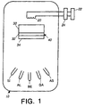
- the preferred embodiment preferably is carried out using a conventional molecular beam epitaxy process within a vacuum chamber 10.
- the chamber includes a conventional electrical coil heater 20 which is connected to a suitable electrical source 22 through a control device 24.
- heater 20 By using heater 20 in a well known manner, the temperature of a substrate 30 can be controlled.
- the substrate comprises GaAs.
- layers such as 32 and 34, are formed on substrate 30.
- the thickness of the layers is exaggerated in Figure 1 so that the layers can be readily seen.
- the layers may be formed of various substances or combinations of substances, such as Be, As, Ga, Al and Si.
- a vacuum chamber of the type shown in Figure 1 is described in more detail in Solid State Electronic Devices, by Ben G. Streetman, (Prentice Hall, 3d Ed. 1990), pp., 19-24, which are incorporated by reference in their entirety into this application.
- defects or impurities are introduced into a compound semiconductor heterojunction bipolar transistor (HBT) wafer comprising substrate 30.
- the defects or impurities are introduced in appropriate densities in, for example, layers 32 and 34, to change the minority carrier lifetime (and related performance characteristics such as device current gain), but not cause other undesirable crystal damage.
- This process represents a controllable, in-process adjustment method that can be electrically monitored and tested on a semiconductor wafer on a lot-by-lot basis.
- a molecular beam epitaxy (MBE) process is carried out by means of the apparatus shown in Figure 1 to produce a solid state electronic device, such as a semiconductor heterojunction bipolar transistor (HBT) 40.
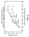
- the growth temperature of the layers is adjusted according to the graph shown in Figure 2 to cause the formation of crystalline defects.
- the concentration of these defects can be reproducibly controlled by adjusting the substrate temperature for each layer by means of heater 20.
- the effect of adjusting the substrate temperature to control beta or gain of the resulting electronic device is shown in Figure 2.
- the horizontal axis of Figure 2 shows a baseline temperature of 0 which corresponds to a range of 520-550 degrees Centigrade (C) and a preferred value of 530 degrees C.
- C Centigrade
- the total range of temperatures represented by the numbers -120 to 0 shown in Figure 2 corresponds to a range of 400-550 degrees C.
- the three lines corresponding to temperatures of the substrate illustrate the gain or beta of a resulting HBT solid state device at a particular device current. The lines tend to converge at the -120 mark on the horizontal axis, thereby indicating that the beta or gain of the resulting device is substantially independent of the current draw of the device.
Landscapes
- Chemical & Material Sciences (AREA)
- Engineering & Computer Science (AREA)
- Crystallography & Structural Chemistry (AREA)
- Materials Engineering (AREA)
- Metallurgy (AREA)
- Organic Chemistry (AREA)
- Physical Deposition Of Substances That Are Components Of Semiconductor Devices (AREA)
- Bipolar Transistors (AREA)
Abstract
A solid state electronic device (40) comprising a substrate (30) and
layers (32 and 34) is fabricated to control the formation of crystalline defects to
control at least one characteristic of the device, such as gain or beta. The
formation of crystalline defects preferably is controlled by controlling the
temperature of the substrate, layers or both.
Description
- The present invention relates generally to fabrication of solid state electronic devices, and more specifically to such fabrication which controls the formation of crystalline defects in such devices.
- Experience has shown a need to control minority carrier lifetime in various solid state devices, including heterojunction bipolar transistors (HBTs). For example, it would be beneficial to produce HBT devices that have consistent current gain so that the circuit yield is high.
- The prior art taught that the introduction of impurities, such as Au, into a high-speed diode can adjust the minority carrier lifetime. Prior HBTs use any of the following: graded, narrow, doped, or stepped base regions to adjust where the minority carriers will recombine. This invention addresses the problems presented by the foregoing prior art and provides a solution.
- The applicants have discovered a method of fabricating a solid state electronic device which is believed capable of controlling minority carrier lifetime. According to the preferred embodiment, the device comprises a substrate and layers. The preferred embodiment controls the formation of crystalline defects in at least one of the layers, whereby at least one characteristic of the device is controlled. For example, the gain or beta of the device can be controlled. Preferably, the formation of crystalline defects is controlled by controlling the temperature of the substrate.
- By using the method, the characteristics of a solid state electronic device can be controlled with a degree of ease and accuracy previously unattainable. For example, the preferred embodiment allows an engineer additional in-process method to control where the minority carriers will recombine to achieve the desired current gain.
-
- Figure 1 is a schematic diagram of a preferred form of molecular beam epitaxy chamber useful for the preferred embodiment of the invention.
- Figure 2 is a graph illustrating the current gain at various device currents resulting from the use of various substrate temperatures during growth of the layers of the type shown in Figure 1.
-
- Referring to Figure 1, the preferred embodiment preferably is carried out using a conventional molecular beam epitaxy process within a
vacuum chamber 10. The chamber includes a conventionalelectrical coil heater 20 which is connected to a suitableelectrical source 22 through acontrol device 24. By usingheater 20 in a well known manner, the temperature of asubstrate 30 can be controlled. In the preferred embodiment, the substrate comprises GaAs. - In a well known manner, layers, such as 32 and 34, are formed on
substrate 30. The thickness of the layers is exaggerated in Figure 1 so that the layers can be readily seen. As shown in Figure 1, the layers may be formed of various substances or combinations of substances, such as Be, As, Ga, Al and Si. A vacuum chamber of the type shown in Figure 1 is described in more detail in Solid State Electronic Devices, by Ben G. Streetman, (Prentice Hall, 3d Ed. 1990), pp., 19-24, which are incorporated by reference in their entirety into this application. - By using apparatus of the type shown in Figure 1, defects or impurities are introduced into a compound semiconductor heterojunction bipolar transistor (HBT)
wafer comprising substrate 30. The defects or impurities are introduced in appropriate densities in, for example,layers - In order to achieve the foregoing result, a molecular beam epitaxy (MBE) process is carried out by means of the apparatus shown in Figure 1 to produce a solid state electronic device, such as a semiconductor heterojunction bipolar transistor (HBT) 40. The growth temperature of the layers is adjusted according to the graph shown in Figure 2 to cause the formation of crystalline defects. The concentration of these defects can be reproducibly controlled by adjusting the substrate temperature for each layer by means of
heater 20. - Similarly, other methods can be used to introduce controlling defects such as impurities. These include ion gauge filaments _ (Figure 1), effusion cells _ (Figure 1), and electron beam evaporation. It is believed that this introduction of defects will change the minority carrier lifetime in the device in a controlled fashion.
- The effect of adjusting the substrate temperature to control beta or gain of the resulting electronic device is shown in Figure 2. The horizontal axis of Figure 2 shows a baseline temperature of 0 which corresponds to a range of 520-550 degrees Centigrade (C) and a preferred value of 530 degrees C. Thus, the total range of temperatures represented by the numbers -120 to 0 shown in Figure 2 corresponds to a range of 400-550 degrees C. As shown in the scale at the top of Figure 2, the three lines corresponding to temperatures of the substrate illustrate the gain or beta of a resulting HBT solid state device at a particular device current. The lines tend to converge at the -120 mark on the horizontal axis, thereby indicating that the beta or gain of the resulting device is substantially independent of the current draw of the device.
- While particular elements, embodiments and applications of the present invention have been shown and described, it will be understood that the invention is not limited thereto since modifications may be made by those skilled in the art, particularly in light of the foregoing teachings. It is therefore contemplated by the appended claims to cover such modifications as incorporate those features which come within the spirit and scope of the invention.
Claims (9)
- A method of fabricating a solid state electronic device comprising a substrate and layers, said method comprising controlling the formation of crystalline defects in at least one of the layers, whereby at least one characteristic of the device is controlled.
- A method, as claimed in claim 1, wherein controlling the formation of crystalline defects in at least one of the layers comprises controlling the temperature of at least one of the members of the group consisting of the substrate and the at least one layer.
- A method, as claimed in claim 2, wherein the method is carried out in a vacuum chamber comprising a heater and wherein the temperature is controlled in a range from 400 degrees C to 550 degrees C, and
wherein controlling the temperature comprises selecting a temperature at which the beta of the device becomes substantially independent of a current draw of the device. - A method, as claimed in claim 1, wherein the characteristic comprises gain or beta at a predetermined device current.
- A method, as claimed in claim 1, wherein the method comprises molecular beam epitaxy.
- A method, as claimed in claim 1, wherein controlling the formation of crystalline defects comprises controlling the impurities of at least one of the layers.
- A method, as claimed in claim 6, wherein controlling the impurities comprises using ion gauge filaments, and/orwherein controlling the impurities comprises using effusion cells, and/orwherein controlling the impurities comprises using electron beam evaporation.
- A method, as claimed in claim 1, wherein said characteristic comprises minority carrier lifetime.
- A product fabricated by the method of claim 1, and comprising a heterojunction bipolar transistor.
Applications Claiming Priority (2)
| Application Number | Priority Date | Filing Date | Title |
|---|---|---|---|
| US09/667,988 US6365478B1 (en) | 2000-09-22 | 2000-09-22 | Solid state electronic device fabrication using crystalline defect control |
| US667988 | 2000-09-22 |
Publications (1)
| Publication Number | Publication Date |
|---|---|
| EP1191579A2 true EP1191579A2 (en) | 2002-03-27 |
Family
ID=24680512
Family Applications (1)
| Application Number | Title | Priority Date | Filing Date |
|---|---|---|---|
| EP01119786A Withdrawn EP1191579A2 (en) | 2000-09-22 | 2001-08-28 | Solid state electronic device fabrication using crystalline defect control |
Country Status (3)
| Country | Link |
|---|---|
| US (1) | US6365478B1 (en) |
| EP (1) | EP1191579A2 (en) |
| JP (1) | JP2002164285A (en) |
Families Citing this family (2)
| Publication number | Priority date | Publication date | Assignee | Title |
|---|---|---|---|---|
| US6569763B1 (en) | 2002-04-09 | 2003-05-27 | Northrop Grumman Corporation | Method to separate a metal film from an insulating film in a semiconductor device using adhesive tape |
| US7474165B2 (en) * | 2005-11-22 | 2009-01-06 | Canon Kabushiki Kaisha | Oscillating device, optical deflector and optical instrument using the same |
Family Cites Families (3)
| Publication number | Priority date | Publication date | Assignee | Title |
|---|---|---|---|---|
| AU7731575A (en) * | 1974-01-18 | 1976-07-15 | Nat Patent Dev Corp | Heterojunction devices |
| US6143631A (en) * | 1998-05-04 | 2000-11-07 | Micron Technology, Inc. | Method for controlling the morphology of deposited silicon on a silicon dioxide substrate and semiconductor devices incorporating such deposited silicon |
| JP2000068284A (en) * | 1998-08-19 | 2000-03-03 | Sharp Corp | Method of manufacturing heterojunction bipolar transistor and power amplifier |
-
2000
- 2000-09-22 US US09/667,988 patent/US6365478B1/en not_active Expired - Lifetime
-
2001
- 2001-08-28 EP EP01119786A patent/EP1191579A2/en not_active Withdrawn
- 2001-08-31 JP JP2001263042A patent/JP2002164285A/en active Pending
Also Published As
| Publication number | Publication date |
|---|---|
| JP2002164285A (en) | 2002-06-07 |
| US6365478B1 (en) | 2002-04-02 |
Similar Documents
| Publication | Publication Date | Title |
|---|---|---|
| EP0430562B1 (en) | Semiconductor heterostructure and method of producing the same | |
| US6365478B1 (en) | Solid state electronic device fabrication using crystalline defect control | |
| US5479028A (en) | III-V system compound semiconductor device and method for manufacturing the semiconductor device | |
| US4233613A (en) | Compound semiconductor wafer | |
| JPH02260628A (en) | Manufacture of semiconductor device | |
| JP2000068284A (en) | Method of manufacturing heterojunction bipolar transistor and power amplifier | |
| JPH02253622A (en) | Manufacture of silicon carbide semiconductor device | |
| TWI360186B (en) | ||
| US4948752A (en) | Method of making sagfets on buffer layers | |
| US7605047B2 (en) | Method for the integration of two bipolar transistors in a semiconductor body, semiconductor arrangement in a semiconductor body, and cascode circuit | |
| KR20060123560A (en) | Meteorological growth method | |
| US5786261A (en) | Method for fabricating semiconductor device having device isolation layer | |
| US7397062B2 (en) | Heterojunction bipolar transistor with improved current gain | |
| KR101082773B1 (en) | Compound semiconductor device and its manufacturing method | |
| WO2004015781A1 (en) | Method for manufacturing compound semiconductor wafer and compound semiconductor device | |
| JPH1074700A (en) | Semiconductor crystal growth method | |
| JP4961740B2 (en) | Method for manufacturing compound semiconductor epitaxial substrate | |
| JP2840381B2 (en) | (III)-Crystal growth method for group V compound semiconductor and crystal growth apparatus used in this method | |
| JPH0529235A (en) | Method for manufacturing GaAs device having high-purity layer | |
| JP2001284363A (en) | Manufacturing method and evaluation method of InGaP / GaAs-HBT | |
| JP3149457B2 (en) | Silicon germanium film, method for manufacturing silicon germanium film, and semiconductor device manufactured using silicon germanium film | |
| US20110227129A1 (en) | Semiconductor substrate, electronic device and method for manufacturing semiconductor substrate | |
| Garcia et al. | Growth characteristics of hydride-free chemical beam epitaxy and application to GaInP/GaAs heterojunction bipolar transistors | |
| JP5543302B2 (en) | Compound semiconductor wafer manufacturing method and compound semiconductor device | |
| JP2646966B2 (en) | Method for growing thin film of III-V compound semiconductor |
Legal Events
| Date | Code | Title | Description |
|---|---|---|---|
| PUAI | Public reference made under article 153(3) epc to a published international application that has entered the european phase |
Free format text: ORIGINAL CODE: 0009012 |
|
| AK | Designated contracting states |
Kind code of ref document: A2 Designated state(s): AT BE CH CY DE DK ES FI FR GB GR IE IT LI LU MC NL PT SE TR |
|
| AX | Request for extension of the european patent |
Free format text: AL;LT;LV;MK;RO;SI |
|
| RAP1 | Party data changed (applicant data changed or rights of an application transferred) |
Owner name: NORTHROP GRUMMAN CORPORATION |
|
| RAP1 | Party data changed (applicant data changed or rights of an application transferred) |
Owner name: NORTHROP GRUMMAN CORPORATION |
|
| STAA | Information on the status of an ep patent application or granted ep patent |
Free format text: STATUS: THE APPLICATION IS DEEMED TO BE WITHDRAWN |
|
| 18D | Application deemed to be withdrawn |
Effective date: 20060301 |